Rashba Spin Splitting in the Al0.6Ga0.4N/GaN/Al0.6Ga0.4N Quantum Well With an Inserted AlxGa1−xN Layer
Abstract
We calculate the Rashba coefficient and Rashba spin splitting for the first subband of the Al0.6Ga0.4N/GaN/Al0.6Ga0.4N quantum well (QW) with an inserted AlxGa1−xN layer. The inserted AlxGa1−xN layer enhances the inherent structure inversion asymmetry (SIA), increases the effective thickness of the GaN triangular potential well, as well as significantly changes the polarization electric field and the electron probability density. Due to the probability density and electric field around the left well (GaN layer) being rather high, contributions to the Rashba coefficient from the left well and the left interface are dominant. These contributions also increase with the Al concentration (x) in the inserted AlxGa1−xN layer. The increasing polarization electric field, combined with the movement of electrons toward the left interface, collectively leads to an increase in both the Rashba coefficient and Rashba spin splitting at the Fermi level as a function of x. Our findings indicate that adding an AlxGa1−xN layer can significantly enhance the Rashba coefficient and Rashba spin splitting in AlGaN/GaN QWs, providing valuable insights for the design of spintronic devices.
PACS number(s):71.70.-d, 73.21.-b, 78.30.Fs
1. Introduction
The manipulation of electron spins in semiconductors has attracted widespread interest as it plays an essential role in the design and manufacturing of spintronic devices [1–8]. To realize spintronic devices, spin splitting of energy bands is of crucial importance, which occurs in systems with asymmetric crystal potentials [9–11]. There are primarily two types of spin-orbit coupling (SOC) that are used to interpret spin splitting: Dresselhaus and Rashba SOC. The former is caused by the bulk inversion asymmetry of crystal potential (BIA) [12], while the latter originates from the structure inversion asymmetry (SIA) of the confinement potential in heterostructures [13, 14]. The SIA and Rashba spin splitting in semiconductor heterostructures can be significantly enhanced by applying internal or external electric fields that are perpendicular to the plane of the two-dimensional system [13–18] or by designing appropriate heterostructures with asymmetric geometric configurations [19–22].
Generally, there are strong spin-orbit effects in narrow-gap materials. For wide bandgap-III nitrides, it is expected that their large band gap will suppress the Rashba spin splitting. However, for AlGaN/GaN heterostructures grown along the c-axis, a large conduction band discontinuity and strong polarization effects at the interface can generate a strong built-in electric field and a high-density two-dimensional electron gas, which will increase the SIA of the heterostructures [23]. Therefore, an inherent SIA exists in the above-mentioned AlGaN/GaN heterostructures even in the absence of external electric fields, making them suitable for evaluating the Rashba spin splitting effect [9, 10, 23–25]. Previous research has investigated the Rashba coefficient and Rashba spin splitting in AlGaN/GaN heterostructures, focusing on factors such as Al content [9, 10, 24], uniaxial strain [26], well thickness [27], gate voltage [28], and conduction band nonparabolicity [29]. Additionally, the wave vector-dependent Rashba coefficient and nonlinear Rashba spin splitting in AlGaN/GaN quantum wells (QWs) [30] are also explored.
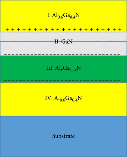
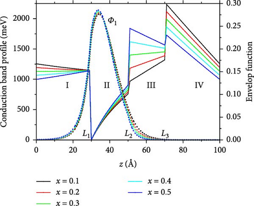
In this paper, we focus on the Al0.6Ga0.4N/GaN/AlxGa1−xN/Al0.6Ga0.4N QWs, which are created by inserting an AlxGa1−xN layer into the Al0.6Ga0.4N/GaN/Al0.6Ga0.4N QW. The schematic diagram of the structure is shown in Figure 1, and the corresponding conduction band profile and the probability density of electrons are shown in Figure 2. The insertion of the AlxGa1−xN layer enhances the inherent SIA of the heterostructure. In Ref. [23], it is shown that the Rashba coefficient and the Rashba spin splitting in the Al0.6Ga0.4N/GaN/Al0.3Ga0.7N/Al0.6Ga0.4N QW can be modulated by changing the relative thickness of the GaN and Al0.3Ga0.7N layers and the external electric field. However, it remains unclear how the Al concentration in the inserted AlxGa1−xN layer affects key factors, such as the polarization electric field, the Fermi level, the electron probability density, and other elements that influence the Rashba coefficient and Rashba spin splitting at the Fermi level. In this article, we found that the presence of the AlxGa1−xN layer significantly affects the polarization electric field, the effective thickness of the GaN triangular potential well, and the electron probability density. Our findings indicate that the contributions to the Rashba coefficient from the left well and the left interface are dominant, and both increase with increasing x. Additionally, we observed that the contribution to the Rashba coefficient from the heterointerface is primarily determined by the electron probability density at the interface. As a result, the Rashba spin splitting at the Fermi level also increases with x due to the enhancement of the polarization electric field within the well and the movement of electrons toward the left interface. These results provide valuable insights for the design of spintronic devices.
The remainder of the paper is organized as follows. In Section 2, the method and the schematic diagram of the structure of the Al0.6Ga0.4N/GaN/AlxGa1−xN/Al0.6Ga0.4N QWs are presented. Section 3 examines the Rashba coefficient and Rashba spin splitting for the first subband at the Fermi level of Al0.6Ga0.4N/GaN/AlxGa1−xN/Al0.6Ga0.4N QWs, discussing in detail the individual factors that influence the Rashba coefficient and Rashba spin splitting. Finally, Section 4 gives a summary.
2. Methodology
Figure 1 illustrates the schematic diagram of the structure of the calculated material, which consists of Ga (Al)-face (0001) Al0.6Ga0.4N/GaN/AlxGa1−xN/Al0.6Ga0.4N QWs. Figure 2 displays the potential profile of the conduction band (V (z)) and the envelope function for the first confined state (Φ1) in the Al0.6Ga0.4N/GaN/AlxGa1−xN/Al0.6Ga0.4N QWs with x = 0.1, 0.2, 0.3, 0.4, and 0.5. As shown in Figures 1 and 2, the Al0.6Ga0.4N/GaN/AlxGa1−xN/Al0.6Ga0.4N QWs, which are grown on top of the substrate, consist of the following regions: the left barrier region (I: LB), the left (II: LW), and right (III: RW) well regions, and the right barrier region (IV: RB). The thickness of the left and right barriers is 30 Å, while the well layer is composed of a 20 Å GaN layer (the left well) and a 20 Å inserted AlxGa1−xN layer (the right well).
Material parameters are as follows. The spin-orbit split-off energy: Δ1 = 22–80x (meV) [35], the crystal-field split energy: Δ2,3 = 6 (meV) [36], and the interband momentum-matrix elements: with E = 20 eV [9, 10].
As noted in Equation (2), the Rashba coefficient for the first subband of Al0.6Ga0.4N/GaN/AlxGa1−xN/Al0.6Ga0.4N QWs consists of seven parts. The contributions to the Rashba coefficient from the left (ГInterL), middle (ГInterM), and right interfaces (ГInterR) correspond to the first three terms. These components are proportional to the electron probability density at the left (L1), middle (L2), and right (L3) heterointerfaces, respectively. They are also related to the eigenenergy E1, potential jumps, and discontinuities in the band parameters at the heterointerfaces. The fourth term in Equation (2) is composed of four parts, where the contributions from the left and right barriers (ГB) correspond to i = I and IV, while the contributions from the left (ГW1) and right (ГW2) wells correspond to i = II and III. They are all equal to the expectation value of BiFi over the ground state envelope function Φ1, which is related to the position-dependent electric field (Fi), the confined energy level E1, and the electron probability density [9, 10, 23–25, 27, 28, 31]. Therefore, the probability density of electrons significantly influences the magnitude of the Rashba coefficient. Once the Rashba coefficient α has been determined, the Rashba spin splitting at the Fermi level can be directly calculated by Δε = 2αkF, where kF is the Fermi wave vector, and it increases with the carrier density.
3. Results and Discussion
We will now calculate the Rashba coefficient and Rashba spin splitting for the first subband at the Fermi level of Al0.6Ga0.4N/GaN/AlxGa1−xN/Al0.6Ga0.4N QWs. We will discuss how the Rashba spin splitting at the Fermi level varies with the Al content of the inserted layer and quantitatively explore the various factors that contribute to the Rashba coefficient and Rashba spin splitting.
As shown in Figure 2, the envelope function of the first subband peaks significantly around the left interface, and both the confining potential and the spatial distribution of electrons in the QW are asymmetric. These asymmetries are induced by the polarized electric field and the inserted AlxGa1−xN layer, which will certainly result in a considerable Rashba coefficient and Rashba spin splitting.
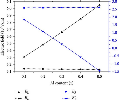
Figure 3a illustrates that when the polarization effect induced by the inserted layer is taken into account, the electric field at the left interface (EL) increases linearly with x, while the electric field at the right interface (ER) decreases in a similar manner. In contrast, if the polarization effect is not considered, the electric field at the left interface (EL’) is reduced, while that at the right interface (ER’) becomes stronger, and both will change more slowly with x. This indicates that the increase (decrease) of the electric field around the left (right) interface is primarily due to the growing polarization effect induced by the inserted layer [28]. For the Ga (Al)-face (0001) AlxGa1−xN/GaN heterostructures, the polarization-induced charges at the interface are positive [24, 37–40]. Consequently, for the Ga (Al)-face (0001) Al0.6Ga0.4N/GaN/AlxGa1−xN/Al0.6Ga0.4N QWs, the polarization charge at the left interface is positive, while the polarization charge at the middle (right) interface is negative, as illustrated in Figure 1. Additionally, if the polarization effect induced by the inserted layer is considered, with increasing x, the amount of negative charge at the middle (right) interfaces increases (decreases) [24, 37–40]. As a result, the electric field in the left well increases and the corresponding potential V (z) becomes steeper, while the electric field in the right well first decreases to zero (V (z) becomes smoother) and then reverses direction and increases in magnitude (V (z) becomes steeper). As a result, the movement of electrons towards the left interface is enhanced, as illustrated in Figure 2, and the probability density of electrons in the left well is further improved by the polarization effect induced by the inserted layer [23].
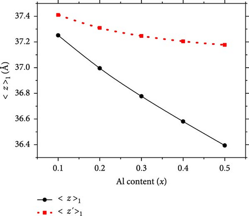
The average position of electrons in the first subband can be defined as: [27, 28], with L being the thickness of the entire Al0.6Ga0.4N/GaN/AlxGa1−xN/Al0.6Ga0.4N QWs. Figure 3b illustrates the average position of electrons in the first subband, where <z >1 (solid lines) represents the scenario considering the polarization effect induced by the inserted layer, and <z’>1 (dotted lines) denotes the case without this effect. As illustrated in Figure 3b, both <z>1 and <z’>1 gradually shift to the left side of the QW with increasing x. This observation is consistent with the findings in Ref. [31]. The reason for this shift is that the potential V (z) of the inserted AlxGa1−xN layer increases with x, causing the peak of the envelope function for the first subband to move toward the left interface, as shown in Figure 2. Moreover, the polarization effect induced by the inserted layer causes the conduction band profile in the left well to become steeper, as shown in Figure 2. Consequently, the peak of the envelope function for the first subband shifts toward the left interface, as illustrated in Figure 3b. As a result, <z>1 is smaller than <z’>1, and <z>1 decreases more rapidly as x decreases. This indicates that the effective thickness of the GaN triangular potential well continuously decreases.
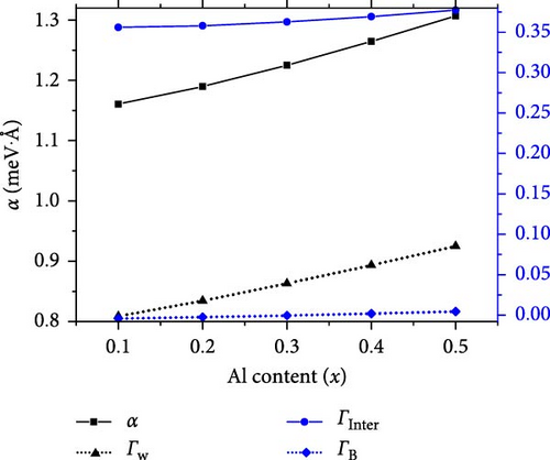
Figure 4a illustrates the Rashba coefficient for the first subband of Al0.6Ga0.4N/GaN/AlxGa1−xN/Al0.6Ga0.4N QWs, along with the contributions from the interfaces (ГInter = ГInterL + ГInterM + ГInterR), the wells (ГW = ГW1 + ГW2), and the barriers (ГB) as a function of x. It is found that the magnitude of α increases linearly with x. Notably, the contribution from the wells is the largest, while that from the interfaces is slightly smaller. As can be seen in Figure 2, the probability of electrons appearing in the barrier and at the right heterointerface is relatively low, leading to minimal contributions to the Rashba coefficient from the barrier (ГB) and the right interface (ГInterR) [23]. Consequently, we only display the contributions to the Rashba coefficient from the left (ГInterL) and middle (ГInterM) interfaces, as well as from the left (ГW1) and right (ГW2) wells in Figure 4b.
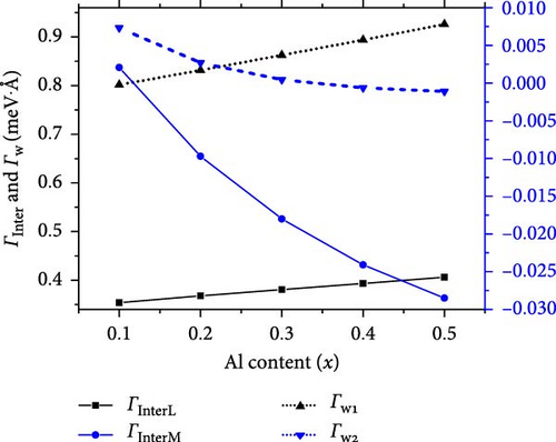
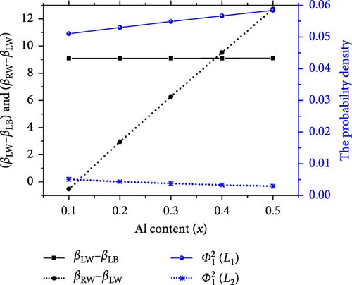
As can be seen in Figure 4b, both ГInterL and ГInterM increase gradually with x, with ГInterL being much larger than ГInterM. To clarify this observation, Figure 4c illustrates (βLW − βLB), (βRW − βLW), and the probability density at both the left () and middle () heterointerfaces as a function of x. As x increases, the peak of the electron probability density shifts towards the left interface, and then the amplitude of the electron probability density at the left and middle interfaces increases, as evidenced by Figures 2 and 4c. Because the higher Al composition (x) results in a larger conduction-band offset, more electrons are transferred into the GaN triangular potential well [24, 31], as seen in Figure 2. Additionally, as shown in Figures 2 and 4c, the electron probability density at the middle interface is an order of magnitude lower than that at the left interface, so ГInterL is much larger than ГInterM. As x increases, (βLW − βLB) remains unchanged, while (βRW − βLW) varies rapidly, with their amplitudes being of the same order. This occurs because the material parameters near the left heterointerface remain unchanged, while those near the right heterointerface vary with x. Therefore, we can conclude that the amplitude of the electron probability density at the middle (left) interface is the dominant factor influencing the amplitude of ГInterM (ГInterL). What’s more, since increases linearly with x, it follows that both ГInterL and ГInter also increase linearly with x.
As illustrated in Figure 4b, ГW1 gradually increases with x, while ГW2 decreases gradually with x, and ГW1 is much larger than ГW2. As previously mentioned, the amplitude of ГW1 (ГW2) is directly proportional to the electric field and the electron probability density in the left (right) well. Figures 2 and 4c show that the electron probability density in the left well is considerably higher than that in the right well. Additionally, the electric field around the left interface is much stronger than that around the right interface, particularly when x is relatively large, resulting in a rather small amplitude of ГW2. Moreover, as x increases, the electric field around the left heterointerface increases linearly (as illustrated in Figure 3a). Consequently, according to Equation (2), both ГW1 and ГW increase linearly. All these factors together result in a linear increase in α as a function of x.
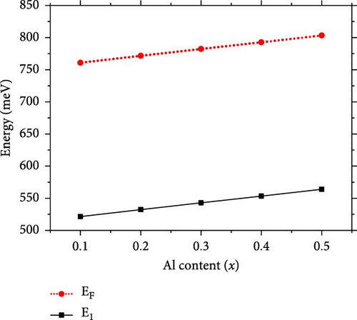
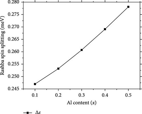
Figure 5 illustrates (a) the Fermi level and the eigenenergy for the first confined state in the Al0.6Ga0.4N/GaN/AlxGa1−xN/Al0.6Ga0.4N QWs with x = 0.1, 0.2, 0.3, 0.4, and 0.5, and (b) the corresponding Rashba spin splitting for the first subband at the Fermi level. We can see that both EF and E1 increase linearly with x, while their difference remains unchanged. As a result, the Fermi wave vector kF doesn’t change. Therefore, the Rashba spin splitting for the first subband at the Fermi level of Al0.6Ga0.4N/GaN/AlxGa1−xN/Al0.6Ga0.4N QWs increases linearly with x, as illustrated in Figure 5b.
Finally, to further investigate the effects of the inserted AlxGa1−xN layer, we calculate the Rashba coefficient and Rashba spin splitting for the first subband at the Fermi level of the Al0.6Ga0.4N/GaN/GaN/Al0.6Ga0.4N QW. The structural parameters of this QW are the same as those of the Al0.6Ga0.4N/GaN/AlxGa1−xN/Al0.6Ga0.4N QWs, except that in the latter, the GaN layer in the right well is replaced by the AlxGa1−xN layer. For the Al0.6Ga0.4N/GaN/GaN/Al0.6Ga0.4N QW, the Rashba coefficient is 1.1321 meV Å−1, and the Rashba spin splitting is 0.2409 meV, which are both lower than those of the Al0.6Ga0.4N/GaN/AlxGa1−xN/Al0.6Ga0.4N QWs. According to Ref. [27], the Rashba coefficient and Rashba spin splitting for the first subband at the Fermi level of the Al0.6Ga0.4N/GaN/GaN/Al0.6Ga0.4N QW decrease as the effective thickness of the GaN triangular potential well increases to a certain extent. Consequently, the effective thickness of the GaN triangular potential well in the Al0.6Ga0.4N/GaN/GaN/Al0.6Ga0.4N QW is much larger than that in the Al0.6Ga0.4N/GaN/AlxGa1−xN/Al0.6Ga0.4N QWs. Therefore, by replacing GaN with AlxGa1−xN in the right well, the effective thickness of the GaN triangular potential well in the Al0.6Ga0.4N/GaN/AlxGa1−xN/Al0.6Ga0.4N QWs decreases as x increases.
In all, as x increases, the inserted AlxGa1−xN layer brings about four main factors that enhance the Rashba spin splitting in the Al0.6Ga0.4N/GaN/AlxGa1−xN/Al0.6Ga0.4N QWs. First, the inherent SIA of the heterostructure is enhanced. Second, the peak of the electron probability density moves towards the left interface because the potential of the inserted AlxGa1−xN layer increases with x. Third, the effective thickness of the GaN triangular potential well decreases as x increases. Finally, the increasing polarization effect caused by the inserted layer leads to an increase (decrease) of the electric field around the left (right) interface.
4. Conclusions
In summary, we calculate the Rashba coefficient and Rashba spin splitting for the first subband at the Fermi level of the Al0.6Ga0.4N/GaN/AlxGa1−xN/Al0.6Ga0.4N QWs. The inserted AlxGa1−xN layer enhances the inherent SIA, makes the electron probability density move towards the left interface, increases the effective thickness of the GaN triangular potential well, increases the polarization effect, and increases (decreases) the electric field around the left (right) interface. As x increases, the peak of the electron probability density shifts towards the left interface, and the average electric field in the well increases. It is found that the electron probability density at the interface is the primary factor that decides the contribution to the Rashba coefficient from the heterointerfaces. Therefore, the two main contributions to the Rashba coefficient come from the left well and the left interface, and both of these contributions increase linearly with x. Moreover, as x increases, the Fermi wave vector kF remains constant. Consequently, the Rashba spin splitting for the first subband at the Fermi level increases linearly with x. The results indicate that the inserted AlxGa1−xN layer can enhance the Rashba coefficient and Rashba spin splitting in AlGaN/GaN QWs. These findings offer valuable insights for the design of spintronic devices.
Conflicts of Interest
The authors declare no conflicts of interest.
Funding
This research was supported by the “316” Project Plan of Xuchang University.
Acknowledgments
This work was supported by the “316” Project Plan of Xuchang University.
Open Research
Data Availability Statement
The datasets used and/or analyzed during the current study are available from the corresponding author on reasonable request.


