
A Flexible Reconfigurable MIMO Antenna for IoT-Enabled Smart Systems
Abstract
As the Internet of Things (IoT) advances, low-cost, intelligently networked wireless sensor networks (WSNs) are being developed and deployed at cloud edge locations to enable new Internet-based services. However, energy consumption in these networked smart sensors is a significant concern. This work focuses on using an ultra-wideband (UWB) multiple-input-multiple-output (MIMO) antenna sensor printed on optically transparent polydimethylsiloxane (PDMS) material to reduce energy consumption in WSN nodes. The antenna sensor structure consists of two rectangular-shaped printed monopole antenna elements (AEs) and four PIN diodes used for switching purpose. A narrow strip is also integrated in the AE to notch WLAN band. The antenna sensor operates in a variety of modes, achieved by varying the ON/OFF states of PIN diodes. The frequency range covered by the antenna is 3.2–11 GHz when all four PIN diodes are turned ON. The overall measurements of the suggested antenna are 31 mm × 31 mm × 1.5 mm. It performs well in terms of diversity, with a minimum isolation of 20.7 dB over the whole operating band. The outcomes of the simulation and the measurements agree fairly well.
1. Introduction
A sensor is a crucial part of a smart device because it can identify any chemical or physical changes in the system and determine when to automate the devices based on the data it has collected and processed [1, 2]. A variety of sensors, gadgets, and nodes that can communicate with one another without the need for human intervention are integrated into the Internet of Things (IoT) [3]. Through the use of fog computing, sensors enable IoT applications that bring the physical and digital worlds closer together [4, 5]. IoT applications use a variety of sensors, including proximity, temperature, humidity, chemical, position, motion, and pressure sensors, to create an environment that is enabled by the IoT [6].
The flexible sensor is capable of identifying biological signals from humans both inside and on the skin. Biomechanical movements, biological signals, and byproducts like useful elements from sweat and body temperature can all be detected by wearable sensors that stick to the skin [7]. In smart agricultural applications, flexible sensors are used to detect soil/water temperature, nitrate, phosphate, and pH [8]. However, environmentally conscious end users and manufacturers want biodegradable versions of energy-autonomous, label-, or sticker-like IoT sensors, which can be used for packaging, logistics, environmental monitoring, and medical diagnostics applications [9]. The substrates of flexible sensors can be developed using a variety of materials, such as polyethylene terephthalate (PET) [10], polyimide [11], and polydimethylsiloxane (PDMS) [12]. Among them, PDMS is employed in this study due of its hydrophobicity, biocompatibility, and affordability. Outstanding interfacial connections are created between the PDMS and the electrodes of the sensors [13]. One major challenge for smart systems is the energy efficiency of wireless sensor networks (WSNs) based on the IoT. The primary cause of this concern is the fact that the WSN subsystem’s nodes is run on tiny batteries or renewable energy sources [14–16].
Several multiple-input-multiple-output (MIMO) antennas for IoT applications have been documented in the literature [17, 18]. A split ring resonator (SRR) in the shape of a ring was added for excellent isolation between the resonating elements in [19], along with a four-port MIMO antenna with a meandering line for improved gain. To improve impedance matching, an eight-port ultra-wideband (UWB) MIMO antenna was constructed in article [20]. The ground plane was designed using the Koch fractal. In paper [21], the antenna design consisted of four UWB monopole elements with an annular ring form, arranged orthogonally. Here, the wideband to narrowband transition was achieved by using PIN diodes in between the feed line and the stepped-impedance resonating stubs. A flexible UWB MIMO antenna with two half-elliptical radiating components fed by coplanar waveguide (CPW) structures was designed in article [22] and was built on a Kapton polyimide substrate. However, these reported antennas were not designed on flexible substrates to be integrated in flexible IoT sensors. They are also not energy efficient and lack a notched band (NB).
- •
Energy efficient: The designed antenna is energy efficient due to the following reasons:
- •
Optically transparent: Since IoT devices are primarily powered by batteries, optically transparent antenna sensors extend their battery life [24]. Also, optically transparent sensors can be easily integrated on the surface of smart devices, without affecting or changing the appearance of those devices [25]. The proposed antenna sensor makes use of a PDMS substrate to meet such requirements.
- •
Easy integrable: The proposed antenna sensor can be easily integrated with PDMS-based sensors for smart bandage [7] and healthcare applications [8] because of the conformal and flexible material used.
- •
Easy fabrication: The proposed antenna adheres easily to the PDMS substrate due to its simple design. PDMS is easy to mold and shape, allowing for simple fabrication of complex structures. It can be cast into intricate patterns and microstructures using soft lithography techniques, making it ideal for wearable electronics [26]. Also, PDMS is a mechanically robust material, providing good support and stability to the antenna design that helps the PCB to withstand physical stress during manufacturing [27, 28].
2. Antenna Structure
Figure 1 depicts the design of the suggested UWB MIMO antenna sensor. The 31 mm × 31 mm antenna is printed on the 1.5 mm thick PDMS substrate with a loss tangent of 0.02 and a relative permittivity of 2.7. The proposed conformal antenna sensor is made from flexible material, which can withstand bending, stretching, and other deformations that occur during normal wear. Also, the lightweight and flexible nature of the conformal antenna sensor allows for greater freedom of movement compared to rigid antennas. This is crucial for applications requiring high mobility, such as sports and fitness tracking.

Four PIN diodes are used to enable switching operation, and two identical rectangular monopole AEs make up the sensor structure. The speed of the switches or diode determines the antenna sensor’s switching speed. The substrate’s bottom surface has a ground plane, and two open-ended slots are added behind the tapered feedline for improved impedance matching. Table 1 displays the dimensions of the antenna sensor design.
| Parameter | Value (mm) |
|---|---|
| L = W | 31 |
| Lg | 8 |
| Lp | 8 |
| Wp | 11 |
| Ld | 20 |
| Wd | 4.5 |
| Wf1 | 1.4 |
| Wf2 | 3.4 |
| g | 0.8 |
| g1 | 1 |
| Ls | 0.8 |
| Ws | 4 |
| Ln | 0.8 |
| Wn | 11 |


To reduce antenna size, various techniques have been used, including loading slots, adding stubs, metamaterials, and fractal geometries [29–31]. Among these, the loading slot is the most popular as it is simpler to implement, fabricate and does not significantly alter the design [32, 33]. Other techniques, such as the use of metamaterials and fractal geometries, complicate the antenna design process [34, 35]. The parametric analysis of loading slot parameters is shown in Figure 4. It is clear from Figure 4(a) that the length (Ls) = 0.8 mm of the loading slot provides wide impedance matching to cover the complete UWB region. However, width (Ws) of the loading slot does not vary with the frequency as presented in Figure 4(b). This shows that Ls has the major impact on the impedance matching as compared to the Ws. The suggested antenna consists of two AEs with switching capability and a notched band. It can be easily integrated with PDMS-based sensors for smart bandage and healthcare applications because of the conformal and flexible material used.


3. Results and Discussion
The constructed prototype of the suggested UWB MIMO antenna sensor fed by 50 Ω microstrip feedlines is depicted in Figure 5(a). While the gain and radiation patterns are examined inside an anechoic chamber (Figure 5(c)), the S-parameters are assessed using a vector network analyzer, as shown in Figure 2(b).

As shown in Figure 6(a), the antenna’s simulated and measured bandwidths are 3–11 GHz and 3.2–10.6 GHz, respectively, and a NB is obtained at the WLAN band. As shown in Figure 6(b), the lowest simulated and tested isolation levels (between two ports) are 18 dB and 21 dB, respectively.


In the suggested antenna, the decoupling structure is designed for a mid-frequency range, as the coupling is stronger at mid-frequencies in simulated isolation (S21) as shown in Figure 6(b). It can be seen in Figure 6(b) that measured isolation at the lower frequencies is lesser than isolation at the higher frequencies because of surface waves and free space radiations at lower frequencies. Still, the measured isolation level is greater than 20.7 dB from 3.2 to 10.6 GHz, which is appropriate for the MIMO antennas.
In the antenna sensor, mirrored AEs with a long stub protruding among them can help achieve better isolation, improving the performance of MIMO algorithms that rely on separating the multiple transmitted and received signals [36–38].
As shown in Figure 6(c), the realized gain in the UWB is from 0 to 7.5 dB. At NB, the measured and simulated gain levels are 3.9 dB and 3.5 dB, respectively. The simulated radiation efficiency varies from 90% to 93% in the UWB range, and it is 35.5% at the NB, as displayed in Figure 6(d).
Figure 7 displays the radiation patterns of the antenna that is being shown at frequencies of 3 GHz, 5 GHz, 7 GHz, and 9 GHz (at φ = 0° and 90°). Bidirectional and omnidirectional radiation patterns are obtained at φ = 0° and 90°, respectively. In almost every radiation pattern, the cross-polarization level is low.


The biasing circuit for the PIN diode is depicted in Figure 8(a). The biasing circuit comprises of a resistor installed on the developed antenna to control the DC biasing current through the PIN diode and a 10 µH inductor that serves as a radio-frequency choke to prevent radio-frequency signals from influencing the DC bias lines. In the ON or OFF state, the PIN diode switches do not behave as an ideal short or open. Figure 8(b) depicts the PIN diode’s RLC equivalent circuit. Inductor (L = 0.5 pH) is linked in series with resistor (R = 1 Ω) when the system is turned ON, and in parallel with C = 0.5 pF and R = 15 kΩ when it is turned OFF.


Table 2 displays various modes of the presented antenna sensor, which are based on the switching of the PIN diodes. In Mode I, all diodes are turned ON, and the presented antenna operates as a two-port WLAN band-notched UWB MIMO antenna sensor, as shown in Figure 3(a). In Mode II, all diodes are turned OFF, which is useful if the antenna sensor needs to be turned OFF without powering down the entire system.
| Modes | Diode ON | Diode OFF | Operation | S-parameters |
|---|---|---|---|---|
| I | D1, D2, D3, D4 | — | MIMO antenna sensor with UWB and WLAN NB | 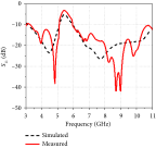 |
| II | — | D1, D2, D3, D4 | Antenna sensor is disabled | 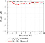 |
| III | D1, D2 | D3, D4 | MIMO antenna sensor with the UWB | 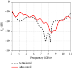 |
| IV | D1, D3 | D2, D4 | Antenna sensor with UWB and WLAN NB | 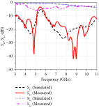 |
| V | D1, D2, D3 | D4 | MIMO antenna sensor with AE-1 having NB and AE-2 without NB | 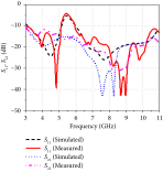 |
In Mode III, diodes D1 = D2 = ON and D3 = D4 = OFF. In this mode, the presented antenna functions as a two-port UWB MIMO antenna sensor. In Mode IV, D1 = D3 = ON and D2 = D4 = OFF. In this mode, the proposed antenna functions as a UWB antenna sensor with WLAN NB. In Mode V, D1 = D2 = D3 = ON and D4 = OFF. In this mode, the proposed antenna operates as a two-port UWB MIMO antenna sensor, with AE-1 having NB and AE-2 without NB.
4. Performance Comparison
Table 3 compares the proposed antenna sensor with recently published MIMO antennas for IoT applications. The table shows that none of the presented antenna designs had NB. The isolation of the proposed antenna is higher than the antenna designs reported in [20, 21, 39, 40]. However, the antenna designs discussed in [19, 20, 39], and [40] were neither energy efficient nor flexible. The antenna in [21] was reconfigurable, which may have saved energy, but it was not flexible enough to be integrated with IoT sensors. Furthermore, the antenna in [22] was flexible, allowing it to be integrated with flexible IoT sensors, but it was not energy efficient. As far as the author is aware, the suggested design is the first energy-efficient two-port antenna sensor configuration since it makes advantage of switching capabilities, optical transparency, UWB and MIMO technology.
| Ref. | Size (mm2)/ports | Substrate | BW (GHz) | NB | Isolation (dB) | Max. gain (dB) | Max. efficiency (%) | Switching | Flexibility | Optically transparent | Energy efficient with flexibility |
|---|---|---|---|---|---|---|---|---|---|---|---|
| [19] | 44 × 44/4 | FR-4 | 1.44, 2.3, 4.2 | No | > 22 | 1 | 67 | No | No | No | No |
| [20] | 54 × 54/8 | FR-4 | 3–12 | No | > 20 | 7.5 | 70 | No | No | No | No |
| [21] | 90 × 90/4 | FR-4 | 3.1–10.6 | No | > 15 | 4.6 | 70 | Yes (frequency, port) | No | No | Energy efficient without flexibility |
| [22] | 100 × 33/2 | Kapton polyimide | 3.2–13 | No | > 23 | 5.5 | 95 | No | Yes | No | Flexible but not energy efficient |
| [39] | 37.6 × 25/2 | FR-4 | 3.5–10.89 | No | > 15.6 | 5.36 | ∼92 | No | No | No | No |
| [40] | 37.6 × 25/2 | FR-4 | 3.3–10.8 | No | > 20 | 5.7 | 96.6 | No | No | No | No |
| This work | 31 × 31/2 | PDMS | 3.2–11 | Yes | > 20.7 | 5.8 | 93.5 | Yes (NB, port) | Yes | Yes | Yes |
Furthermore, the antenna sensor can be easily integrated with PDMS-based sensors for smart bandage and healthcare applications because of the conformal and flexible material used. Despite the compact size, the AEs achieve good radiation efficiency. This is important for ensuring strong signal transmission and reception, particularly in low-power applications. The planar structure of the antenna sensor contributes to a low-profile design, which is aesthetically pleasing and practical for embedding in smart wearable devices.
5. Conclusion
This research presents a two-port UWB MIMO antenna sensor that is energy-efficient and has switching functionality. Rectangular radiators with tapered feedlines and a partial ground plane with open-ended slots behind the feedlines characterize the proposed antenna. The AE and NB switching is accomplished by PIN diodes. The antenna sensor that is being shown has five switching modes. In terms of bandwidth, gain, efficiency, and isolation, the antenna performs well. The proposed design is easy to build, integrates with PDMS-based IoT sensors with ease, and is energy-efficient. Therefore, the suggested antenna may be a good option for PDMS-based sensors that are employed in agricultural and smart bandage applications.
Conflicts of Interest
The authors declare no conflicts of interest.
Author Contributions
S. conceived and performed the simulations and drafted the manuscript. G.S. and S.K. conducted the experiment. S.A., W.E.-S., and B.G. analyzed the results. S.K.P. investigated the experimental results and revised the manuscript. All authors reviewed the manuscript.
Funding
The authors would like to extend their gratitude to King Saud University (Riyadh, Saudi Arabia) for funding this research through Researchers Supporting Project number (RSP2024R260).
Acknowledgments
The authors would like to extend their gratitude to King Saud University (Riyadh, Saudi Arabia) for funding this research through Researchers Supporting Project number (RSP2024R260).
Open Research
Data Availability Statement
The data that support the findings of this study are available from the corresponding author upon reasonable request.