A Lumped-Element Directional Coupler for Bandwidth Enhancement, Impedance Matching, and Harmonic Suppressions
Abstract
This paper presents a lumped-element wideband directional coupler that enables arbitrary impedance matching and harmonic suppressions from 2f0. The coupler consists of four filtering networks (FNs) and an asymmetric branch-line hybrid serving as the matching network. The use of lumped-element topology helps reduce circuit size and improve harmonic suppressions. Each FN, composed of two lumped-element resonators, contributes two additional transmission poles, enabling bandwidth scaling, bandwidth enhancement, and harmonic suppressions. To demonstrate the effectiveness of the proposed design, a wideband coupler with various terminal impedances operating at 0.5 GHz is designed, simulated, and fabricated. The measured size is , the fractional bandwidth for –14.3 dB return loss is 46%, and the harmonic suppression is more than –30 dB from 0.69 to 4.5 GHz.
1. Introduction
Directional couplers are essential components in wireless communication systems as they provide power division with proper phase differences between two outputs. However, traditional branch-line couplers, comprising four 90° transmission-line sections (TLs), suffer from drawbacks such as large circuit space occupation and high-order harmonics that can interfere with other devices. To mitigate these issues, additional low-pass filters are often used to eliminate unwanted harmonics. Previous attempts have been made to address these challenges using combinations of TLs and inductors [1], parallel-shorted and open stubs [2], parallel TLs [3], dual-open/short-stub loaded resonator [4, 5], coupled lines [6], and lumped-element topologies [7]. However, these approaches have only achieved narrow harmonic-suppression bandwidths, limiting their practical applications.
There have been extensive researches on multifunctional multiport components in recent literatures [1–18]. This is because cascading multiple microwave components can lead to increased circuit area, fabrication complexity, and insertion loss in the radio frequency front end. These components have been studied for various applications such as dual/multiband performance [8–13], wideband filtering performance [14, 15], and arbitrary impedance matching [16–18]. However, the couplers proposed in [8–16], which are based on microstrip-line structures, are limited by their large circuit sizes. On the other hand, in [17, 18], lumped-element couplers with real/complex impedance matching are only suitable for narrow bands due to their low fractional bandwidths.
In recent years, there has been a growing need for miniaturization and bandwidth extension in modern wireless communication systems. To achieve a reduction in circuit size, the composite right-left handed (CRLH) unit is utilized to replace traditional transmission line (TL) branches, as demonstrated in articles [19, 20]. Ultraminiaturized wideband bandstop filters and miniaturized wideband bandpass filters with frequency-dependent complex source and load have been realized using integrated passive devices (IPD) technology in [21, 22]. Additionally, an ultraminiaturized wideband power divider utilizing generalized quasi-Chebyshev and -elliptic low-pass filtering networks has been reported in [23].
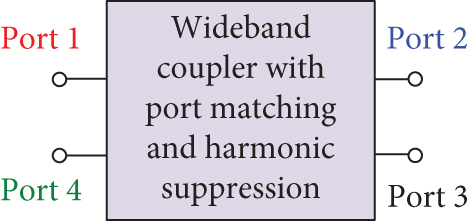
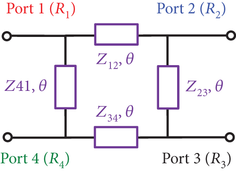
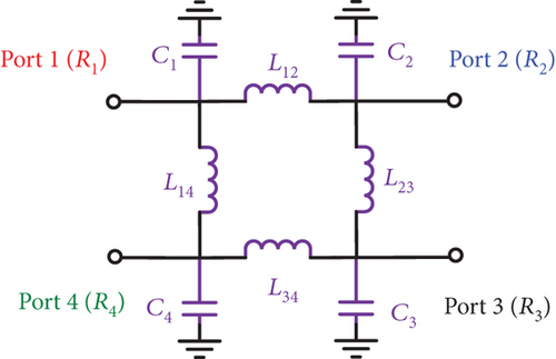
In this paper, a novel lumped-element coupler, as shown in Figure 1(a), is proposed. It is equivalent to a traditional branch-line coupler, four impedance matching network, and four filters as depicted in Figure 1(b). The coupler is synthesized using an asymmetric branch-line hybrid and designed filtering networks (FNs). The filtering networks provide variable bandwidths, which are controlled by a bandwidth control factor described in Section 2.3. In this study, a circuit-based simulation using the schematic feature of the Advanced Design System (ADS) software was employed in Section 2, while a full-wave simulation utilizing the Momentum simulation in microwave mode of ADS software was conducted in Section 4. This design theory addresses the common impedance mismatch in circuits by integrating impedance matching, eliminating the need for additional circuits and thereby reducing design complexity and losses. While primarily for theoretical validation at 0.5 GHz, this work can operate across various frequencies and is applicable in fields like the Beidou System and satellite telephony. To the best of the authors’ knowledge, there are only a few previous works that have focused on branch-line couplers with wideband, controllable bandwidth, compact size, wideband harmonic suppressions, and arbitrary impedance matching.

2. Analysis of the Proposed Coupler
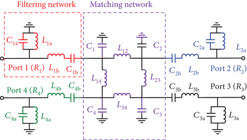
Figure 2 shows the schematic of the proposed lumped-element wideband coupler for arbitrary impedance matching and harmonic suppressions. This proposed coupler essentially consists of four sets of filtering networks (FNs) and a matching network (MN).
2.1. Matching Network
2.2. Filtering Network
For further improving the harmonic suppressions and expanding the bandwidth, a filtering network composed of a series inductance and capacitance resonator and shunt inductance and capacitance resonators is loaded on the four ports of the matching network.
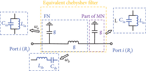
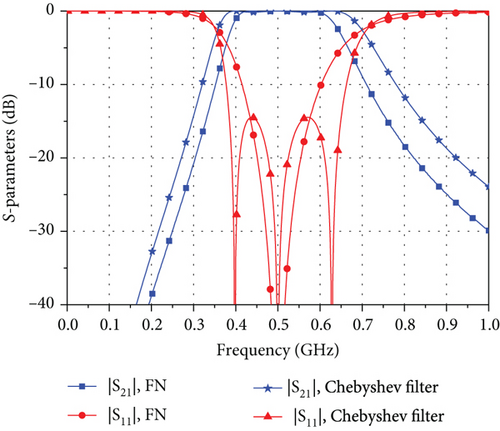
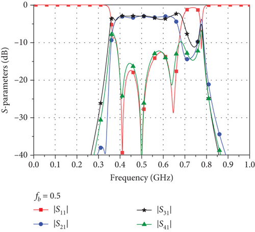
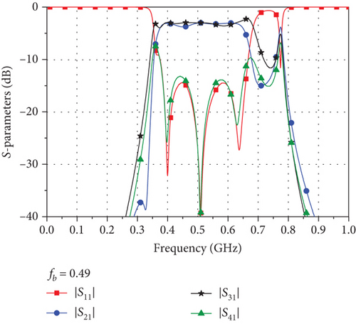
To achieve the desired functions, including impedance matching and tunable fractional bandwidth (FBW), the four ports are analyzed separately, as shown in Figure 4(a). A portion of the matching network (MN) can be equivalently represented as a parallel combination of capacitors and inductors, which, when connected in series with the filtering network (FN), forms an equivalent Chebyshev filter. As depicted in Figure 4(b), the FN itself has only one pole. However, when a part of the MN is equivalent to capacitors and inductors similar to those in the FN and then connected in series with it, three poles are achieved.
| Matching network | |||||||
|---|---|---|---|---|---|---|---|
| Pra. | Sim. | Mea. | Pra. | Sim. | Mea. | ||
| L12 (nH) | 12.33 | 11 | 11 | C1 (pF) | 12.72 | 12 | 12 |
| L23 (nH) | 21.35 | 20 | 22 | C2 (pF) | 12.96 | 12 | 12 |
| L34 (nH) | 19.17 | 18 | 18 | C3 (pF) | 9.94 | 9 | 8 |
| L41 (nH) | 22.51 | 22 | 24 | C4 (pF) | 9.70 | 9 | 8 |
| Filtering network | |||||||
|---|---|---|---|---|---|---|---|
| Pra. | Sim. | Mea. | Pra. | Sim. | Mea. | ||
| L1a (nH) | 7.32 | 8.7 | 8.7 | L3a (nH) | 10.98 | 12 | 12 |
| C1a (pF) | 13.84 | 12 | 12 | C3a (pF) | 9.22 | 8.2 | 8.2 |
| L1b (nH) | 34.60 | 33 | 33 | L3b (nH) | 51.89 | 51 | 51 |
| C1b (pF) | 3.05 | 3.1 | 3.0 | C3b (pF) | 2.03 | 1.9 | 1.9 |
| L2a (nH) | 8.78 | 9.5 | 9.5 | L4a (nH) | 14.64 | 16 | 16 |
| C2a (pF) | 11.53 | 10 | 10 | C4a (pF) | 6.92 | 6.8 | 6.8 |
| L2b (nH) | 41.52 | 39 | 39 | L4b (nH) | 69.20 | 68 | 68 |
| C2b (pF) | 2.54 | 2.5 | 2.4 | C4b (pF) | 1.52 | 1.4 | 1.4 |
2.3. The Bandwidth Control Factor (B)
The ideal simulated S-parameters of the proposed coupler for various B are shown in Figure 7. For both return loss and isolation, it can be seen that the extra two TPs are located at 0.40 and 0.61 when B = 0.4. When B = 0.5, the extra two TPs are located at 0.395 and 0.645. When B = 0.6, the extra two TPs are located at 0.375 and 0.675. Thus, it can be calculated that the fractional bandwidths (FBWs) between two transmission poles are 40%, 50%, and 60% at center frequency f0 = 0.5 GHz, respectively, which is equal to the specified values of B.
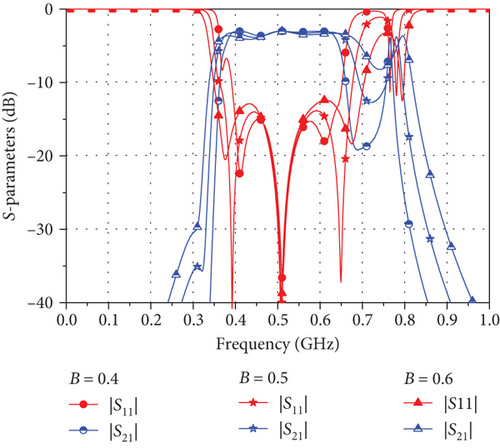
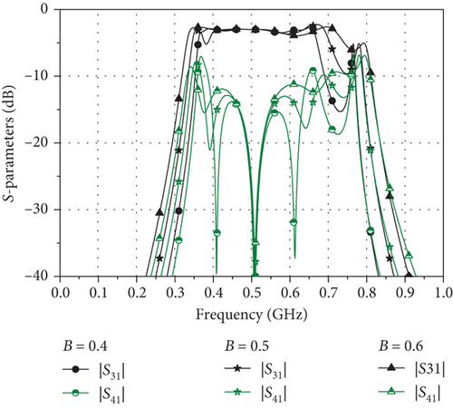
It can be concluded that, since the value of B is approximately equal to the FBW between the two poles of return loss and isolation, the desired bandwidth can be easily achieved by selecting appropriate B.
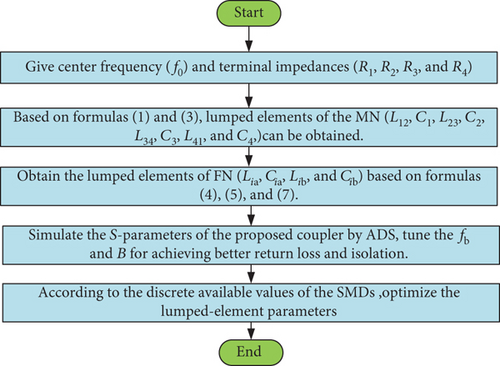
3. Design Procedure
- (1)
Specify the desired specifications including the center frequency (f0) and the terminal impedances (R1, R2, R3, and R4) of the four ports
- (2)
Then calculate the lumped elements (L12, C1, L23, C2, L34, C3, L41, and C4) of the matching network using equations (1) and (3).
- (3)
Select the initial value of B according to the desired bandwidth and calculate the lumped elements of FN (Lia, Cia, Lib, and Cib) based on equations (4), (5), and (7). Construct the circuit model and simulate the S-parameters of the proposed coupler in Figure 2 by the ADS software and tune the fb for achieving better return loss and isolation. If the specifications cannot be met, please reselect proper B
- (4)
According to the dimensions and discrete available values of the surface-mounted devices (SMDs) of the lumped inductors and capacitors, build the transmission-line feeding pad and optimize the lumped-element parameters
4. Experimental Validation
To demonstrate the validity of the design theory obtained from the previous analysis, a lumped-element wideband coupler with the design specifications setting as f0 = 0.5 GHz, k = 1, R1 = 50 Ω, R2 = 60 Ω, R3 = 75 Ω, R4 = 100 Ω, fb = 0.49, and B = 0.46 are simulated, manufactured, and measured using RO4350 (εr = 3.66, h = 1.524 mm) substrates. Ideal simulated S-parameters of the proposed coupler are shown in Figure 6(b). The final layout and the photograph of the fabricated lumped-element coupler are displayed in Figures 9 and 10. The circuit size is 14.5 mm × 14.3 mm.
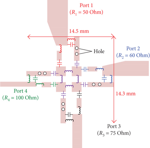

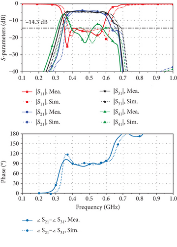
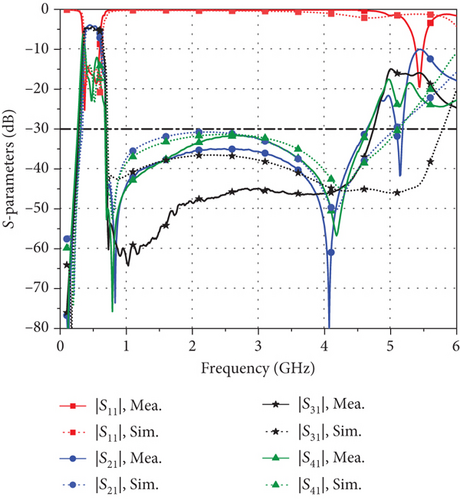
Figure 11 shows the results of the full-wave simulation and the final measurement. To account for the inevitable tolerance and discrete available values of the SMDs of lumped inductors and capacitors, the design parameters were fine-tuned; however, there is still some small deviation and slight frequency shift (0.2 GHz) between the simulated and measured frequency responses. The simulated and measured values of the proposed coupler are summarized in Tables 1 and 2. In contrast, the performances of the proposed coupler and several state-of-the-art couplers are tabulated in Table 3.
| Refs. | f0 (GHz) | FBW (%)/|S11| (dB) | PD. | AI. | Harmonic suppression area | Electrical size () | Technology |
|---|---|---|---|---|---|---|---|
| [1]1 | 1 | ~50/–15 | 4 : 1 | No | 2f0 − 4f0 (–40 dB) | 0.17 × 0.30 | Microstrip + SMD |
| [3] | 1 | 9/–20 | 1 : 1 | No | 2f0 − 4f0 (–15 dB) | 0.19 × 0.19 | Microstrip |
| [2] | 3 | 30.5/–15 | 2.5 : 1-10 : 1 | No | 2f0 (–15 dB) | 0.5 × 0.47 | Microstrip |
| [7]2 | 1 | 4/–15 | 1 : 1 | Yes | X | 0.06 × 0.06 | SMD |
| [11] | 0.83 | 38.5/-10 | 1 : 1 | No | 2f0 (–20 dB) | 0.07 × 0.06 | Microstrip |
| [14] | 3.5 | 61.1/–15 | 31.6 : 1 | No | X | 0.39 × 0.84 | Microstrip |
| [12] | 1.63/2.73 | 7.5/5.13 | 1 : 1 | No | 5.2f1 (-19.5) | 0.25 × 0.25 | Microstrip |
| This work | 0.48 | 46/–14.3 | 1 : 1 | Yes | 2f0 − 9f0 (–30 dB) | 0.039 × 0.039 | SMD |
- 1Prototype II; 2Case B; 33 dB bandwidth. PD.: power division ratio; AI.: arbitrary impedance matching; λg: the guided wavelength at the center frequency.
As shown in Figure 11(a), with the measured center frequency 0.48 GHz, the measured return loss is greater than –14.3 dB from 0.36 to 0.58 GHz, with 46% FBW. The measured insertion losses (∣S21∣ and ∣S31∣) are –4.2 dB and –4.4 dB at center frequency, and the maximum amplitude imbalance between Port 2 and Port 3 (∣S21 | –∣S31∣) of ±1 dB has also been achieved from 0.38 to 0.58 GHz, with 42% FBW. Furthermore, the measured phase difference between Port 2 and Port 3 (∠S21–∠S31) deviates within ±10° over the range of 3.7 to 6.0 GHz, with 48% FBW. As the ∣S21∣ (∣S31∣) and ∣S12∣ (∣S13∣) exhibit almost identical characteristics, only the graphs for ∣S21∣ and ∣S31∣ are displayed. The comparison data shows that it is the first fully lumped-element-based coupler to achieve such bandwidth.
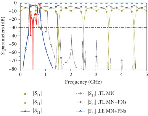
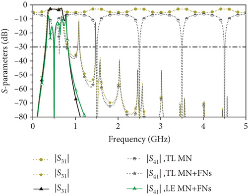
Figure 11(b) illustrates the measured result from 0 to 6 GHz with 0 to –80 dB. Seen that over –30 dB measured harmonic suppressions for insertion loss (∣S21∣ and ∣S31∣) and the isolation (∣S41∣) are realized from 0 to 0.26 GHz, and from 0.69 to 4.63 GHz (from 2f0 to 9f0), respectively. In the ideal model, the resonant zero observed at 0.75 GHz arises from the resonance between capacitors in the MN and inductors in the FN, leading to the noted harmonic. However, the absence of the resonant zero in measurement and EM simulation can be attributed to increased parasitic resistance within the feeding pad and SMDs, which reduces the Q factor, along with the mismatch between commercially available component values and their idealized counterparts used in circuit simulations. This harmonic effect also can potentially be mitigated by optimizing the layout during EM simulations or by refining the MN network.
According to the comparison data, this work uniquely achieves wideband harmonic suppression from 2f0 to 9f0 with more than –30 dB suppression, while maintaining a remarkably compact size. This achievement is a first in similar designs. Additionally, this work effectively addresses the common issue of narrow bandwidth in lumped-element couplers. Compared to other lumped-element couplers [7], it achieves a tenfold increase in bandwidth and features the capability of arbitrary port impedance. Furthermore, it exhibits significant bandwidth advantages over other structures with the same power distribution ratio and offers flexibility in bandwidth adjustment through parameter tuning. This work achieves a 58% [7] to 99% [14] reduction in electrical size compared to other couplers, indicating its exceptionally compact structure.
The proposed lumped-element coupler theory can reduce PCB size through the application of SMD devices at low frequencies. Additionally, in situations where fabricating transmission lines is impractical, the use of commercial SMD components offers a cost-effective and space-saving solution, while also simplifying the layout optimization process. At high frequencies, the lumped elements can be integrated into chips such as integrated passive devices (IPD) and low-temperature cofired ceramics (LTCC) to reduce the overall area of the chip. Looking ahead, utilizing high-Q (quality factor) SMD components can enhance the circuit’s performance, and optimizing the chip layout to achieve the desired values of lumped elements presents a significant challenge.
5. Conclusion
In this paper, for the first time, a fully lumped-element-based coupler with controllable large fractional bandwidth, arbitrary impedance matching, and wideband harmonic suppressions from 2f0 has been proposed utilizing MuRata SMDs. Good agreement between EM simulation and measurement demonstrates that the proposed multifunctional coupler is of great potential to reduce the system complexity, circuit size, and fabrication cost of the future RF front-end design.
Conflicts of Interest
The author declares that he has no conflicts of interest.
Acknowledgments
This work is supported by the School of Integrated Circuits, Beijing University of Posts and Telecommunications.
Open Research
Data Availability
The data used to support the findings of this study are included within the article.


