A Comparative Study of Coprecipitation and Solvothermal Techniques for Synthesizing Pure and Cu-Doped SnO2 Nanoparticles
Abstract
Tin oxide (SnO2), with its low resistivity properties and high transparency in the visible spectrum, makes it an attractive electron transfer layer (ETL) for use in perovskite solar cells. Here, we use two techniques, coprecipitation and solvothermal, to synthesize pure and 4% copper-doped SnO2. The X-ray diffraction patterns revealed that the films synthesized using both methods have a crystalline structure with a tetragonal arrangement. Furthermore, the lack of any secondary peaks indicated the absence of mixed tin oxide (Sn2O4) or copper oxide (CuO) components. Additionally, it demonstrated that adding a 4% Cu doping concentration reduced the crystal size in both methods. The optical results indicate adequate transmission in the central range of the visible spectrum. Calculations were performed to find the energy gap of pure SnO2 in both techniques to be 3.85 eV and 4.17 eV, respectively. When we doped SnO2 with 4% Cu, this band gap energy decreased to 3.75 eV and 3.9 eV. Furthermore, with 4% Cu doping, the particle size decreases, as demonstrated by FESEM. The EDX spectroscopy images revealed that the synthesized nanoparticles consisted of copper, oxygen, and tin. The analysis of functional groups using Fourier transform infrared (FTIR) spectra and the roughness analysis using AFM images showed a decrease in roughness from 46.1 nm to 12.3 nm in doped samples prepared by solvothermal synthesis, compared to those synthesized by the coprecipitation technique from 4.7 nm to 0.3 nm. We discovered that Cu plays an essential role in reducing nanocrystalline SnO2 particle sizes. In addition, the solvothermal technique is more impressive than coprecipitation in the synthesis of tin oxide nanostructure.
1. Introduction
The investigation of SnO2 thin films is of considerable interest owing to their distinctive and appealing characteristics, including excellent optical transmittance, uniformity, nontoxicity, elevated conductivity, chemical inertness, resistance to thermal degradation, mechanical reliability, piezoelectric capabilities, and cost-effectiveness [1]. Because it can better sense gases, let a lot of visible light through, and reflect strongly infrared wavelengths, SnO2 is a type of semiconductor called an n-type metallic semiconductor. Additionally, it exhibits a substantial gap at normal room temperatures and has an excitation binding energy of around 130 meV [2, 3]. Researchers have identified SnO2 as an exceptionally promising material for electron transport layers in perovskite solar cells due to its extraordinary properties. There are good band gap sites, wide band gaps between 3.6 and 4.5 eV, high electron mobilities of 240 cm2 V−1 s−1, which is about 100 times higher than TiO2, and higher carrier concentrations than 1015 cm3 [4–6]. To get the desired characteristics for particular applications, it is essential to control the size, shape, and doping concentration of NPs during the synthesis process [7,8].
Doping SnO2 nanostructures with particular metals can greatly modify their optical, electrical, and magnetic properties [9]. Researchers have employed various doping elements such as copper, zinc, nickel, lanthanum, and cobalt to adjust the characteristics of SnO2 nanoparticles [10, 11].
The doped material should have increased photocatalytic activity due to the decreased activation energy and rearrangement rate of e−-h+ couples. Cu is a crucial transition metal because it can narrow the band gap and thus extend the absorption of light from both UV and visible regions while also serving as a growth inhibitor [12]. However, many research reports show lower solubility of Cu, indicating the occurrence of the oxide form of Cu crystals as heterojunctions [13]. On the other hand, doping of Cu in SnO2 also induces lattice defects, and oxygen vacancies considerably improve the photocatalytic efficiency under visible light [14, 15].
Many methods for the fabrication of SnO2 nanostructures have been developed, ranging from lithographic technologies to chemical methods [16]. Various chemical methods such as the coprecipitation method have emerged as a novel economically viable technique with large-scale production capabilities, simplicity and rapid synthesis, low cost, high sample purity, numerous prospects to customize the particle surface, low pressure, low temperatures, and chemical homogeneity compared to other methods [17]. The authors of [18, 19] revealed that this method has various advantages such as easy control over the crystalline size, stoichiometry, and surface morphology of prepared samples that help to control the physical and chemical properties of the samples. However, the solvothermal method with an aqueous solvent as a reaction medium is environmentally friendly because the reactions are carried out in a closed system. Hydrothermal synthesis involves the use of water as a solvent at elevated temperatures and pressures in a closed system, and certain properties of the solvents such as density, viscosity, and diffusion coefficient change [20, 21]. Furthermore, hydrothermal synthesis is often used due to its simple processes and equipment, without high temperature sintering, allowing the control of the grain size, morphology, and degree of crystallinity through easy changes in the experimental procedure [22]. In 2022, Goswami and his team [23] prepared SnO2 and they successfully fabricated SnO2 nanocrystals with high crystallinity by using Cu as a dopant. This was due to the energy band gap of SnO2 being quite wide, resulting in small absorbent waves. These factors necessitate the addition of tin oxide to other impurities, commonly known as dopants [24]. Chen et al. [25] found that Cu doping reduced the SnO2 crystal lattice with the preferred growth along the (110) plane for the high Cu concentration. It has high electrical and thermal conductivity [26]. In addition to doping, factors that impact the quality of the thin layer of tin oxide include the spin coating method, which has attracted significant interest due to its numerous advantages: simple, low temperature growth, [27] uniform thin films to flat substrates and its low cost [28].
The aim of this study is to find the best way to make pure and Cu-doped SnO2 nanoparticles that are highly crystallized, easily dispersed, and have a uniform particle size distribution. We also examine the fundamental structural, optical, and morphological characteristics of the films through the use of XRD, UV-visible spectroscopy, FESEM, EDX, FTIR, and AFM analysis.
2. Experiment
2.1. Materials and Chemicals
We purchased tin (IV) chloride pentahydrate (SnCl4 5 H2O, Merck, 99.9%), liquid ammonia (NH3, 25%, Merck, India), and copper (II) acetate monohydrate (Cu(CO2CH3)2·H2O, 99%) from Sigma-Aldrich to produce both pure and 4% Cu-doped SnO2. Ethanol (C2H6O) and Milli-Q double-distilled water are used as solvents for preparation and purification in the synthesis process.
2.2. Preparation of Samples
Glass slides, FTO-coated glass, quart slides, and silicon wafers were first cleaned with Mill-Q double-distilled water and then ultra-sonicated with ethanol for 15 min. They were then dried with air.
To achieve pure SnO2 NPs, measure 5.912 g of tin (IV) chloride pentahydrate (SnCl4.5H2O) and dissolve it in a beaker containing 100 mL of a mixture of double-distilled water and ethanol in a 1 : 1 ratio to prepare a solution with a molarity of 0.1 and stir it for 40 minutes using a magnetic stirrer. Then liquid ammonia (NH3) was added dropwise into the initial solution until the pH reached 9.6 of the solution with continuous stirring for 20 minutes at 300 rpm on a magnetic stirrer to create a transparent solution.
Preparation of 4% of Cu as a dopant: dissolve 4 grams of copper (II) acetate monohydrate in less than 100 ml of distilled water in a beaker. Transfer the solution to a 100 ml volumetric flask and increase the volume to 100 ml with Milli-Q double-distilled water. Conversely, copper doping (4%) influences the electrical conductivity of SnO2 NPs, resulting in a transparent and conductive layer suitable for use as an ETM in perovskite solar cells [27].
2.3. Coprecipitation Technique
As a dopant source, copper (II) acetate monohydrate [Cu(CH3COO)2.H2O] was added to half of the precursor solution (SnCl4.5H2O). The reaction was then stirred magnetically for thirty minutes to complete it. We also raised the pH of the solution to 9.6 by gradually adding small amounts of aqueous ammonia (25%) solution while continuously stirring the mixture. Next, we vigorously stirred the mixture, heated it to 50°C for two hours, stored the final result at room temperature for 24 hours, and washed it five times with double-distilled water and ethanol (1 : 1) to remove any ammonia and chloride impurities.
2.4. Solvothermal Technique
Another half of the previous precursor solution SnCl4.5H2O (0.1 molarity) was subjected to continuous magnetic stirring for half an hour at 300 rpm to preserve chemical homogeneity, and 0.1 M of an aqueous solution of ammonia was gradually introduced until the pH level reached 9.6. We agitated the solution for 10 minutes before transferring it into a 50 mL Teflon autoclave, then placed the autoclave inside an oven, and exposed it to reaction temperatures of 200°C for 24 hours. Following a preestablished duration, cool the reactor to room temperature and carefully remove the white or creamy-white precipitates from the beaker. The required amount of dopant solution, [Cu(CH3COO)2.H2O], was slowly introduced drop by drop with continuous magnetic stirring, and the pH was stabilized at 9.6 by introducing aqueous ammonia, and then the solution was vigorously stirred and heated to 50°C for two hours. We performed a series of five rinses on the final solution using double-distilled water and ethanol (1 : 1) to eliminate any ammonia and chloride substances.
2.5. Spin Coating Deposition
Spin coating (spin rate = 3000 rpm for 45 seconds) was used to deposit the precursor solution to create pure and 4% Cu-doped SnO2 thin film nanostructures using both techniques on thoroughly cleaned glass slides, quartz slides, silicon wafers (100), and FTO-coated glass substrates, and then these nanostructures were dried at 60°C on a hot plate for 30 s to yield a clear, homogeneous, and transparent solution, repeating this process three times. All the samples were annealed for one hour at 160°C in an oven and then cooled to room temperature. The annealing of samples at 160°C was used for a possible chemical reaction that takes place on the heated surface to produce SnO2 and Cu-doped SnO2 thin film may be as follows: when the droplets of the aqueous solution reached the heated substrate, chemical reaction of tin chloride with water vapor of solutions, stimulated by the temperature, takes place providing the formation of SnO2 films and also Cu doped SnO2 with the formation of oxides through some intermediate products [1].
2.6. Characterization
The synthesis of pure and 4% Cu-doped films has been studied using XRD and UV-visible spectra. The morphology and elemental composition of the films were investigated using FESEM, EDX, and FTIR analyses. Finally, atomic force microscope (AFM) was used to detect nanoscale size, morphology, surface texture, and roughness.
3. Results and Discussion
3.1. X-Ray Diffraction
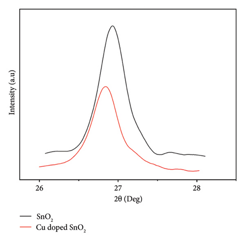
The XRD patterns of pure SnO2 and SnO2 with 4% Cu added were made using the coprecipitation method, as shown in Figure 1(a). The patterns show the rutile form phase of SnO2 with a tetragonal structure, which is in agreement with the reported values from the JCPDS card (98-003-9178). This phase exhibits a preferred orientation along the (110), (111), (011), (11), (130), and (031) directions. As nanostructures develop along their specific growth directions, we frequently observe the most noticeable peak (110). The standard values of SnO2 NPs closely align with the observed peaks. It is important to mention that the XRD patterns do not exhibit any secondary peaks associated with the CuO or mixed Sn2O4 phase. This shows that adding copper (Cu) does not change the crystal structure of pure SnO2. This demonstrates the successful substitution of Cu ions in SnO2. The results are in agreement with [25, 26, 29, 30]. Furthermore, Figure 1(b) displays the diffraction peaks shifted towards the lower angle as the copper concentration is introduced. This indicated that Cu2+ ions have been incorporated into the crystal lattice of SnO2, thereby developing lattice strain within the host crystal lattice [31, 32]. The inclusion of copper within the SnO2 lattice has the potential to generate additional nucleation sites. Reduced crystal growth leads to a corresponding increase in lattice strain. This phenomenon would reduce the crystallinity of doped SnO2 samples.
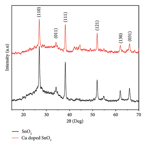
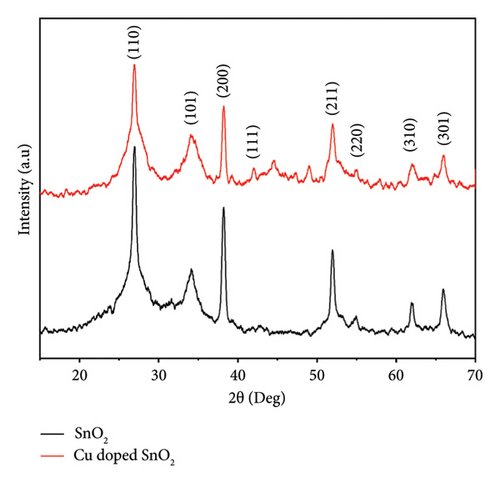
On the other hand, Figure 1(c) displays the XRD results of the solvothermal technique. The diffraction reflections exhibited a strong correlation with the tetragonal rutile structure of SnO2, as evidenced by their alignment through JCPDS: 41–1445. The undoped and 4% Cu-doped SnO2 NPs exhibit comparable dominant crystallographic planes, namely, (110), (101), (200), (111), and (211), with the most prominent peak observed at (110) coordinates. We detected no supplementary characteristics linked to Cu/CuO.
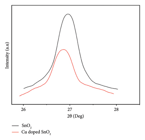
The introduction of a 4% Cu dopant concentration results in a drop in the overall intensity of the peaks and a shift in the (110) SnO2 plane (Figure 1(d)), which confirms the incorporation of dopants in the crystal lattice and broadens the peaks. This observation indicates a reduction in both particle size and crystallinity. The result corroborates well with the previous results [5, 25, 33], which revealed that the absence of noise peaks indicates that the SnO2 nanoparticles exhibit a high degree of crystallinity.
The particle sizes measured in the coprecipitation technique are 12.2 nm and 10.6 nm for pure and Cu-doped SnO2 NPs, respectively. The literature [15, 17, 36] has reported a comparable pattern of alteration in crystal size for pure and 4% Cu-doped SnO2. The inclusion of Cu2+ ions into the Sn site inhibited the growth process, as indicated by the observed reduction in crystal size of SnO2 with 4% Cu doping levels. Furthermore, the presence of Cu2+ ions in the host lattice promotes the creation of extra nucleation sites, thereby increasing the lattice strain and impeding the crystal development process [15, 36]. On the other hand, the solvothermal method produced nanoparticles that were 4.8 nm in pure SnO2 and 4.6 nm in 4% Cu-doped SnO2. The presence of defects in the system caused a deflection of the diffraction angle. This deflection resulted in a decrease in the distance between the atomic levels, as described by Bragg’s rule (nλ = 2d sinθ). Consequently, the FWHM (β) increased, as indicated by Scherrer equation (1) [26, 37].
Solvothermal techniques formed the SnO2NPs, which are slightly smaller and more delicate than those created by co-precipitation techniques. In addition, the co-precipitation samples had fewer clumped structures and smaller average crystallite sizes than the copper-containing samples. They also had more clumped structures and a smaller average crystallite size than the copper-containing samples made using coprecipitation.
3.2. Visible Absorption Spectra
For both methods, the UV-visible spectra were measured for both pure SnO2 and SnO2 that had Cu added to it. We did this to see how the optical band gap changes as the Cu amount is added. Figures 2(a) and 2(b) show the transmission (T%), which has been obtained by UV-visible spectra at 200–800 nm, and the transmission edges for pure SnO2 were 92.26 nm and 94.20 nm, showing the nanocrystalline impact of the films. Also, the transmission edges of Cu-doped SnO2 films were 70.77 nm and 90.07 nm, respectively, which led to shifts towards the low-energy red shift. When the film is pure SnO2, the transmittance is at its highest point, but it decreases with the addition of 4% Cu. It is found that transmittance decreases with increasing concentration of the dopant [38], leading to an increase in the film’s absorption coefficient and an increase in the density of the defects because the decrease in optical transmission is clearly obtained in the spectrum. The reduction in transmittance is related to the point defects induced by Cu dopant. Higher optical absorption or lower transmittance could be originated by the optical transitions from the occupied 3d band to the 4s–4p band of the Cu point defects [39].
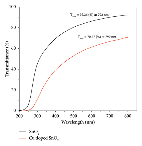
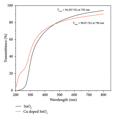

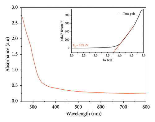
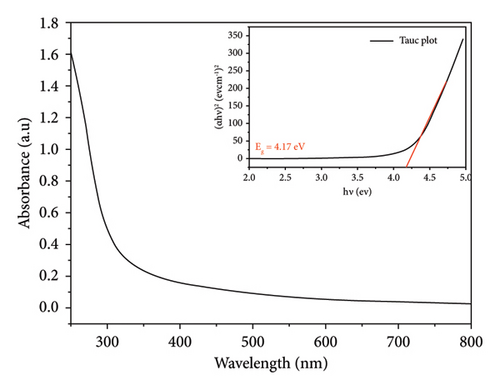
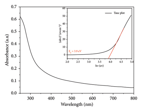
It is important to point out that the decreased band gap of SnO2 NPs created using the solvothermal technique indicates their ability to capture a larger portion of visible light. The visible band gap of SnO2 varies depending on the synthesis procedure and distortion effect. This distortion effect may arise due to two reasons; either Cu is creating levels nearby conduction band or incorporation of Cu producing oxygen vacancies which are making levels nearby conduction band [29].
3.3. FESEM and EDX Analysis
FESEM was applied to characterize the morphologies and structures of both undoped and Cu-doped SnO2 NPs synthesized by coprecipitation and solvothermal methods. Figures 5(a) and 5(b) show representative FESEM images of undoped and Cu-doped SnO2 samples obtained using the coprecipitation procedure. This FESEM image displays tetragonal-sized SnO2 NPs that have a relatively uniform size. The phenomenon of agglomeration is contingent upon the dimensions of the particles. As particle size approaches the nanoscale, aggregation increases. The average particle size of 11.6 nm was determined using FESEM.
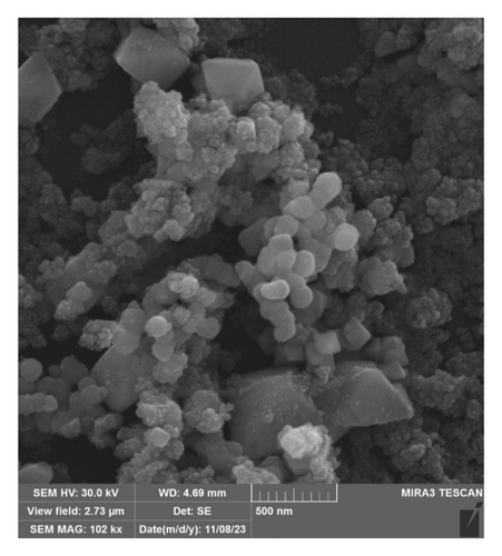
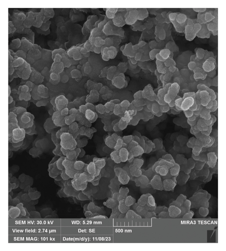


The FESEM image (Figures 5(a) and 5(b)) reveals that the synthesized samples consist of uniformly distributed particles with nearly similar sizes. The addition of Cu-doped tin oxide reduces the particle size, as measured by ImageJ, from 11.6 nm to 10.3 nm, as shown in Figures 5(c) and 5(d). The substitution of tin ions with copper ions inside the structure explains the reduction in size. This is due to the fact that the copper atom is smaller than the tin atom. The results are similar to those of earlier studies [15, 26], which showed that Cu-doped SnO2 can be divided into two different types: substitutive and interstitial. Copper plays an important role in inhibiting the development of the SnO2 material. The introduction of Cu in the SnO2 material leads to a higher stacking fault energy, which is responsible for the increased nucleation sites [15].
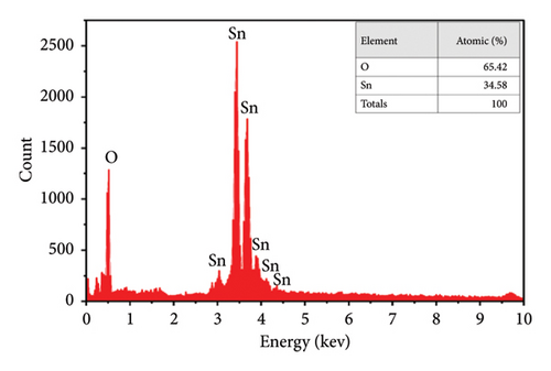
The energy-dispersive X-ray (EDX) test in the coprecipitation technique was used on different parts of the samples, which confirmed that the nanocrystals’ composition was pretty uniform. The EDX analysis of the pure sample, as shown in Figure 5(e), provides conclusive evidence of the presence of tin and oxygen. The observed intensity peak of oxygen is comparatively lower than that of Sn, indicating that the oxygen atoms have undergone desorbed processes. This phenomenon is associated with the rise in oxygen vacancies [46], and the spectra obtained from the doped sample (Figure 5(f)) demonstrate the successful integration of Cu2+ ions into SnO2, as well as the rising peaks of Sn, O, and Cu [52]. In addition, Diviya et al. [17] demonstrated that the spectra of the doped samples provide evidence of the insertion of Cu2+ ions into the SnO2 lattice. Also, the acquired findings nearly resemble the initial stoichiometry.
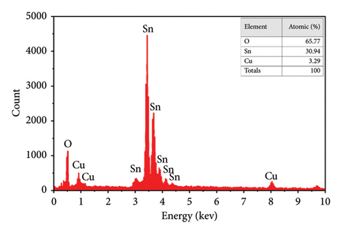
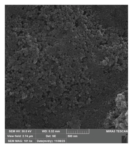
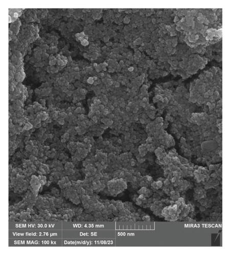
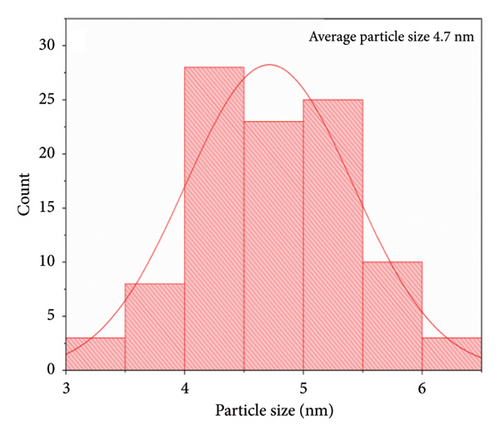
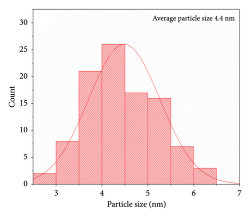
Using the solvothermal method, Figures 6(a) and 6(b) show the shapes of the pure SnO2 NPs and those with 4% Cu added to them. However, the morphology of the SnO2 NPs underwent changes with increasing Cu doping concentration and the particles were agglomerated with semisimilar sizes. The nanocrystalline sizes of these two samples were obtained by ImageJ from FESEM and Cu-doped tin oxide reduced the particle size from 4.7 nm to 4.4 nm as shown in Figures 6(c) and 6(d). The concentrations of dopants influenced the increased physical bonding between the particles at the nanoscale, leading to the agglomeration of particles with similar sizes [5]. The rate of nucleation and growth processes has an impact on both the grain size distribution and the amount of agglomeration [53, 54].
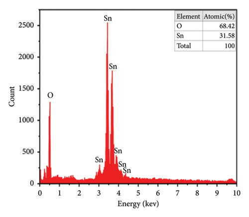
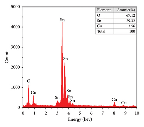
The quantitative analyses of the deposited films are carried out by EDX, and images are shown in Figures 6(e) and 6(f). In the spectrum, there are two strong peaks corresponding to Sn and O which confirm the purity of the SnO2 thin films. From EDX images, it is observed that the height of the peak for Sn decreases while that for Cu increases with an increase of the Cu doping. This indicated that the Cu2+ replaced some of the Sn4+ in the SnO2 lattice to form a solid solution phase [25, 55].
3.4. Fourier Transform Infrared (FTIR) Spectra
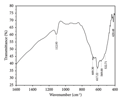
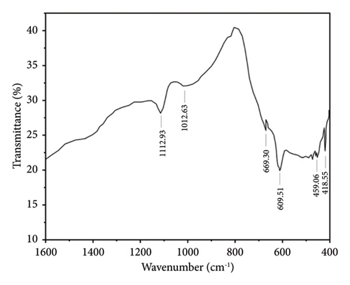
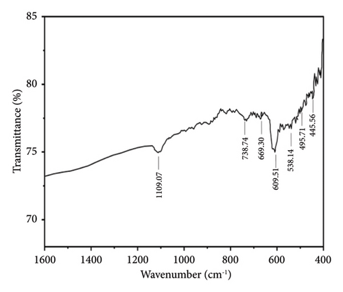
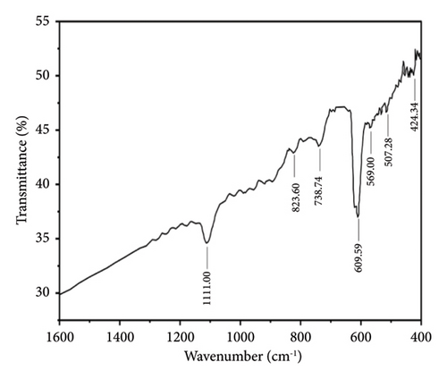
Figures 7 and 8 show the FTIR analysis conducted between wavelength spectra of 1600 to 400 cm−1 for pure and 4% Cu-doped SnO2 NPs synthesized by coprecipitation and solvothermal techniques. The absorption frequency spectral bands are indicative of the vibration modes displayed by the films. The occurrence of peaks at 670 and 520 cm−1 is closely associated with the O-Sn-O antisymmetric stretching mode bridge of SnO2 functional groups, as determined by the coprecipitation technique (Figure 7(a)). The peak of 609 cm−1 indicates the existence of Cu elements, as shown in Figure 7(b), and the observed phenomena can be attributed to the lattice mode. The Cu2+ ions are replaced inside the Sn-O lattice; consequently, the peaks of maximum absorption exhibit a shift towards higher wavenumbers, and the result matches [17]. The FTIR study confirmed the presence of the SnO2 lattice mode, the most dominant among all identified peaks. Also, in the solvothermal method, an observable broad peak is detected at a wavelength of 609.51 cm−1. The spectral range spanning from 738 to 445 cm−1 has been attributed to the vibrations of Sn-O. Figure 8(a) denotes the skeleton Sn-O vibrations associated with the SnO2 structure. In addition, the inclusion of copper, as depicted in Figure 8(b), leads to various alterations, and the host lattice causes a shift of the Sn/Cu-O skeletal vibrations and an increase in the intensity of the absorbed bands. As the Cu content increases, the absorbed zone on the surface of the nanoparticles increases [56]. The existence of the Cu: SnO2 lattice mode was confirmed using FTIR analysis, which revealed a highly dominant set of peaks.
3.5. Surface Roughness Study
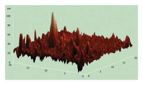
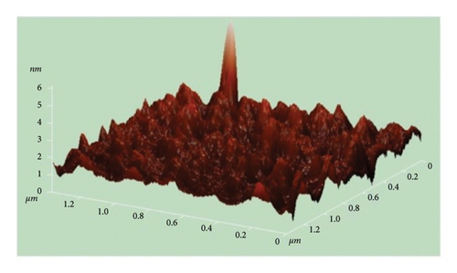
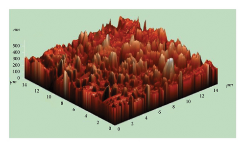
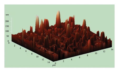
The atomic force microscope (AFM) technique was used to analyze the surface morphology of pure and Cu-doped SnO2 thin films fabricated by both procedures. Figures 9(a), 9(b), 9(c), and 9(d) display three-dimensional AFM images acquired using high scan mode. The difference in surface roughness between the pure and 4% Cu-doped SnO2 thin films is easily noticeable. Table 1 displays the values of the root mean square roughness (RMS) and the average roughness (AR) for all films. The values of RMS and AR decreased from 7.3 to 0.4 nm and from 4.7 to 0.3 nm when Cu was added in the coprecipitation technique, respectively. The root mean square (RMS) surface roughness is frequently used to analyze surface morphology, plays a significant role in light scattering phenomena, and provides valuable insights into the surface quality for the purpose of optical device design [57]. Also, in the solvothermal technique, RMS and AR decreased from 61.5 to 21.3 nm and 46.1 to 12.3 nm as 4% Cu was added. The increase in the surface roughness of SnO2 film from solvo-hydrothermal is higher than that of the coprecipitation technique; this can be attributed to an increase in layer thickness [58].
| Techniques | Samples | Root mean square (nm) | Average roughness (nm) | Average grain size (nm) | |
|---|---|---|---|---|---|
| XRD | FESEM | ||||
| Coprecipitation | Pure SnO2 | 7.3 | 4.7 | 12.2 | 11.6 |
| Cu-doped SnO2 | 0.4 | 0.3 | 10.6 | 10.3 | |
| Solvothermal | Pure SnO2 | 61.5 | 46.1 | 4.8 | 4.7 |
| Cu-doped SnO2 | 21.3 | 12.3 | 4.6 | 4.4 | |
4. Conclusion
Coprecipitation and solvothermal techniques are two effective ways to make pure and Cu-doped SnO2 NPs. In both methods, the XRD data confirmed the tetragonal crystal structure of SnO2. The inclusion of Cu did not alter the structure of the crystal (SnO2), but the introduction of Cu dopant in both methods resulted in a decrease in the average size of the crystallites. The optical studies demonstrated that the introduction of Cu to the SnO2 lattice resulted in a decrease in the band gap energy. Additionally, the films formed using solvothermal methods exhibited higher transparency compared to those prepared through coprecipitation methods. The integration of Cu2+ ions into the host lattice, which leads to the formation of extra energy levels inside the band gap, is responsible for the decrease in the Eg. The FESEM picture from the coprecipitation method showed that pure SnO2 NPs that are tetragonal in shape have an average particle size of 11.6 nm, and the introduction of Cu in the SnO2 reduced the particle size to 10.3 nm. Furthermore, the solvothermal technique revealed that both the undoped and Cu-doped samples reduced the particle size from 4.7 nm to 4.4 nm. FTIR studies confirmed that the SnO2 lattice mode is present, and that all identified peaks are strongly dominant and the spectral range spanning from 738 to 445 cm−1 has been attributed to the vibrations of SnO2 in both techniques. The AFM picture shows that the increase in the surface roughness of SnO2 film from solvo-hydrothermal is higher than that of the coprecipitation technique; this can be attributed to the increased thickness of the film layers. As 4% Cu was added, the RMS value dropped from 7.3 nm to 0.4 nm and the AR value dropped from 4.7 nm to 0.3 nm in the coprecipitation method and from 61.5 nm to 21.3 nm and 46.1 nm to 12.3 nm in the solvothermal method.
Conflicts of Interest
The authors declare that they have no conflicts of interest.
Acknowledgments
The authors express their gratitude to Salahaddin University for providing partial financial support and to the Scientific Research Centre of Erbil Polytechnic University for letting them use their laboratory.
Open Research
Data Availability
The data utilised to substantiate the conclusions of this study may be obtained from the corresponding author upon request.


