Study on the Electronic Structures and Optical Properties in Four Directions of Si-NWs Modified by Oxygen Atoms
Abstract
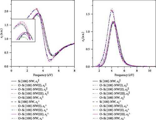
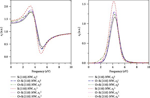
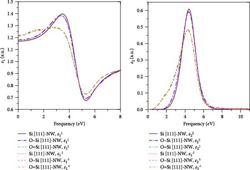
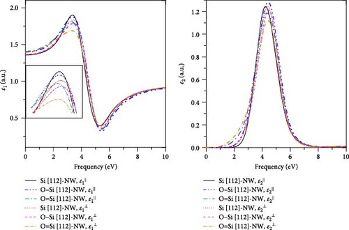
In this work, the first-principles study based on density functional theory was applied to investigate the geometries, electronic structures, and optical properties in four directions of the Si-NWs surface, which are modified by oxygen atoms. The results show that the geometries, band structures, and optical properties of the Si-NWs are affected by the modification of oxygen atoms. The Si─Si bonds adjacent to the region modified by oxygen atoms elongate, the cell volumes decrease, while the energy gaps of Si-NWs narrow. Evident impurity bands appear on the energy bands of the modified Si-NWs, forming S═O double bonds. A blue shift of the perpendicular component spectra of the dielectric constant relative to parallel spectra can be observed for Si [100]-NW, Si [111]-NW, and Si [112]-NW. At the same time, the real and imaginary parts of the dielectric function spectra of all Si-NWs are red-shifted after the modification by oxygen atoms, and the spectra of Si [111]-NWs forming Si═O double bonds are the most significant red-shifted. These results can provide a theoretical reference for preparing nano-silicon optoelectronic materials and devices.
1. Introduction
As early as 1964, Wagner and Ellis [1] first reported the growth mechanism of Si-NW, but due to experimental conditions and technical limitations, research progress on Si-NW was slow in the following decades. Until Liber reported in 1998 on the growth of Si-NW with a diameter in the range of tens of nanometers, the research on Si-NW has developed rapidly [2, 3, 4, 5, 6, 7]. Because of their excellent mechanical, thermal, electrical, and optical properties, Si-NWs have attracted extensive research attention in the fields of material science and chemistry [4, 8, 9, 10, 11, 12, 13]. Holmes et al. [14] experimentally showed that Si-NWs grown along different crystal directions exhibit different luminescence characteristics. Theoretical research also indicated that the energy gap characteristics of Si-NWs depend on the nanowire orientation, demonstrating a significant impact of the Si-NWs direction on their electronic structure [15, 16, 17, 18]. At the same time, Dong et al. showed that the surface modification exerts a certain effect on the electronic structure and optical properties of Si-NWs [19, 20, 21]. In addition, Canham [22] reported in 1990 that porous silicon prepared by anodic oxidation could emit visible light at room temperature, and it was established that nano-silicon oxide could effectively improve the luminous efficiency of silicon materials. Both Wolkin of Rochester University, who investigated the electronic state and luminescence of porous silicon quantum dots, and academician Qin of Peking University, who studied the photoluminescence mechanism model of oxidized porous silicon and nano-silicon embedded silicon oxide [23, 24], indicated that oxidation could improve the luminous efficiency of silicon nanostructures.
Besides many studies on oxidized Si-NWs, there are no reports on the effects of the bonding mode of Si and O atoms on the electronic structure and optical properties of Si-NWs in different directions. In this work, the first-principles method based on density functional theory (DFT) is used to study the electronic structure and optical properties of oxygen-modified Si [100], Si [110], Si [111], and Si [112] nanowires, showing distinct effects of different bonding behaviors on the electronic structure and optical properties of Si-NWs. These results provide a theoretical reference for preparing nano-silicon and silicon-based optoelectronic devices.
2. Model and Calculation Method
As shown in Figure 1, Si-NWs are considered in four directions, i.e., [100], [110], [111], and [112]. Then, one Si atom on the Si-NW surface is replaced by an O atom or two hanging bonds of Si atom(s) on the Si-NW surface are passivated by an O atom, and finally, H atoms are used to passivate other hanging bonds on the Si-NWs surfaces. Among them, Si [100]-NWs substitution doping occurs at positions I and II, which are represented by O─Si [100]-NW (I) and O─Si [100]-NW (II), respectively. The passivated surface refers to establishing a Si─O─Si bridge bond between positions I and II, or a Si═O double bond on the Si atom at position II, which are represented by O─Si [100]-NW (III) and O═Si [100]-NW, respectively. Then, Si [110]-NW, Si [111]-NW, and Si [112]-NW substitution dopings occur at position I, forming a Si─O─Si bridge bond, represented by O─Si [110]-NW, O─Si [111]-NW, and O─Si [112]-NW, respectively. One O atom passivates the surface of the Si atom at position I to form a Si═O double bond, represented by O═Si [110]-NW, O═Si [111]-NW, and O═Si [112]-NW, respectively. Periodic boundary conditions are selected here. The periodic structure is taken along the nanowire direction. To avoid the influence caused by periodic boundary conditions, a vacuum layer with a thickness of 2 nm is added between the nanowire and its periodic mirror.
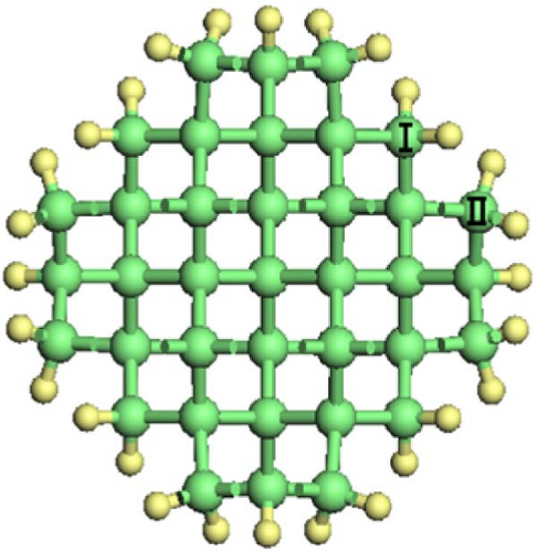
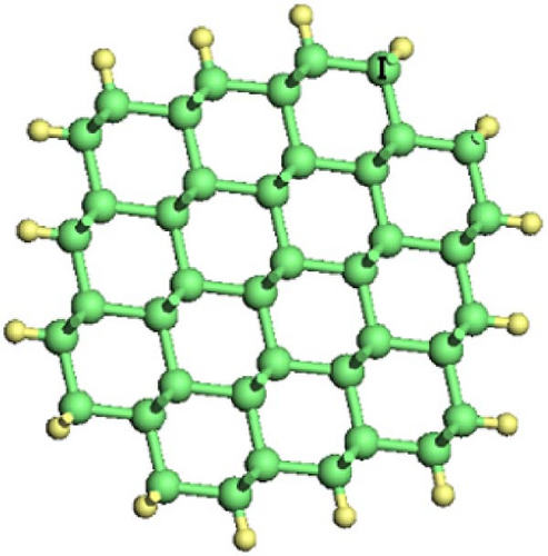
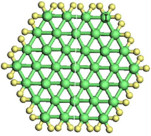
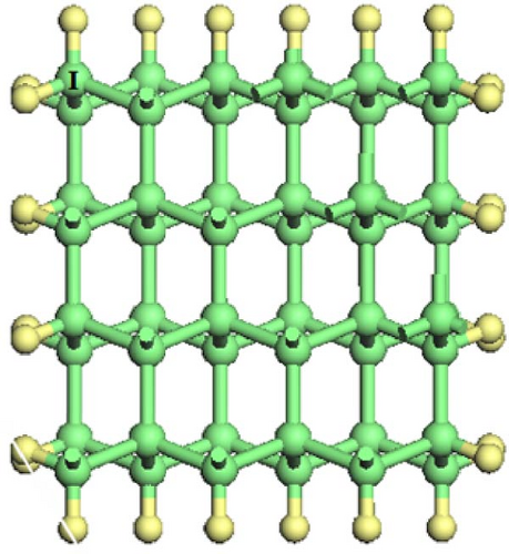
In this work, the first-principles method based on DFT is used to calculate the electronic structure and optical properties of Si-NW [25, 26]. The ultra-soft pseudopotential plane wave method and the Perdew–Burke–Ernzerh functional under generalized gradient approximation (GGA) are selected as the exchange-correlation potential functional, and the plane-wave truncation energies are set to 380 eV. In the structural optimization process, the self-consistent convergence accuracy is 1 × 10⁻⁵ eV/atom, the internal stress convergence standard of the crystals is 0.05 GPa, and the maximum displacement convergence standard of the atoms is 0.001 Å. The grid size of k points in the Brillouin zone is taken as 1 × 1 × 3. Based on optimization, norm-conserving pseudopotential, and the Perdew–Burke–Ernzerh functional under GGA are selected as the exchange-correlation potential functional, and the truncation energies are set as 600 eV.
3. Results and Discussion
3.1. Geometry Optimization
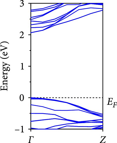
The geometries of Si-NWs in four directions modified by O atoms are optimized. Then, the bond length between Si─Si atoms, the bond length between Si─O atoms, and the cell volume sizes in Si-NWs were obtained, as shown in Table 1. Before the modification by O atoms, the Si─Si bonds in the internal regions of Si [100]-NW, Si [110]-NW, Si [111]-NW, and Si [112]-NW are longer, with values of 0.2377, 0.2381, 0.2371, and 0.2376 nm, respectively. In contrast, the Si─Si bonds in the surface regions of nanowires are shorter, with values of 0.2347, 0.2353, 0.2348, and 0.2349 nm, respectively. These results are in good agreement with the Si─Si bond length of 0.235 ± 0.002 nm reported by Kajiyama et al. [27]. The Si─Si bond lengths in different regions of Si-NWs are different, mainly because the surface atoms are affected by the surface effect, resulting in the shortening of surface bonds, while the internal atoms of nanowires are less affected, maintaining the bulk Si characteristics. After being modified by O atoms on the surface of Si-NW, the lengths of Si─Si bonds near the Si─O bond region are elongated, while the lengths of Si─Si bonds in other regions far away from Si─O remain the same. The main reason is that the length of the Si─O bond is shorter than that of the Si─Si bond, resulting in a smaller cell volume after O modification. At the same time, the Si─Si bond near the Si─O bond is elongated. In addition, the Si─O bond length of Si-NWs is greatly affected by the bonding form, and the formed Si─O─Si bridge bonds are longer, while the formed Si═O double bonds are shorter. This shows that the Si═O double bond structure is more stable than the Si─O─Si bridge bond structure.
| Si-NW | DSi─Si (nm) | DSi─O (nm) | V (nm3) | Bandgap (eV) |
|---|---|---|---|---|
| Si [100]-NW | ||||
| Si [100]-NW | 0.2347–0.2377 | — | 0.0073490 | 2.066 |
| O─Si [100]-NW (Ⅰ) | 0.2347–0.2414 | 0.1671 | 0.0072122 | 1.922 |
| O─Si [100]-NW (Ⅱ) | 0.2344–0.2389 | 0.1678 | 0.0072299 | 1.935 |
| O─Si [100]-NW (Ⅲ) | 0.2346–0.2383 | 0.1658 | 0.0072918 | 1.948 |
| O═Si [100]-NW (Ⅳ) | 0.2348–0.2383 | 0.1537 | 0.0072466 | 1.684 |
| Si [110]-NW | ||||
| Si [110]-NW | 0.2353–0.2381 | — | 0.0080698 | 1.144 |
| O─Si [110]-NW | 0.2345–0.2381 | 0.1668 | 0.0080137 | 0.991 |
| O═Si [110]-NW | 0.2352–0.2381 | 0.1535 | 0.0080669 | 0.931 |
| Si [111]-NW | ||||
| Si [111]-NW | 0.2348–0.2371 | — | 0.0158638 | 1.659 |
| O─Si [111]-NW | 0.2325–0.2404 | 0.1673 | 0.0154053 | 1.601 |
| O═Si [111]-NW | 0.2349–0.2371 | 0.1538 | 0.0158303 | 1.398 |
| Si [112]-NW | ||||
| Si [112]-NW | 0.2349–0.2376 | — | 0.0069714 | 1.712 |
| O─Si [112]-NW | 0.2349–0.2453 | 0.16780 | 0.0068579 | 1.721 |
| O═Si [112]-NW | 0.2350–0.2376 | 0.15380 | 0.0069712 | 1.600 |
3.2. Electronic Structure
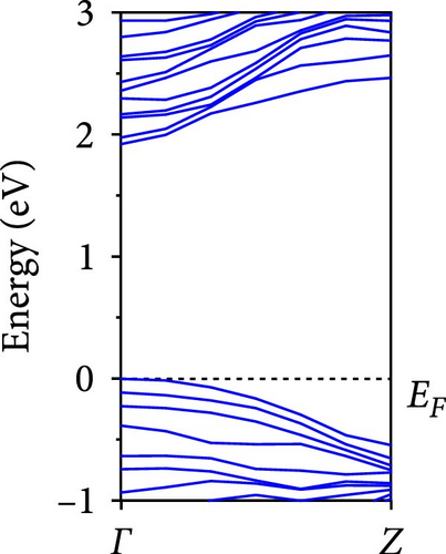
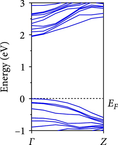
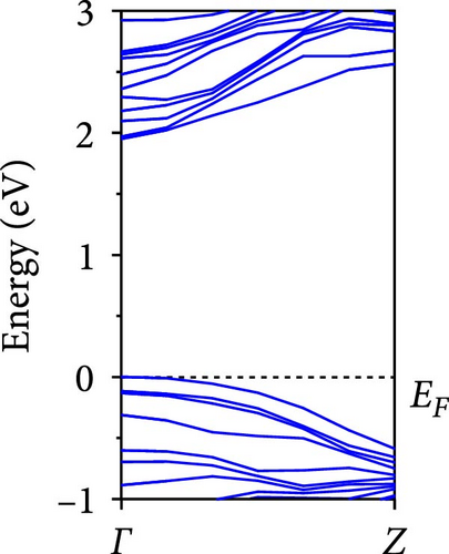
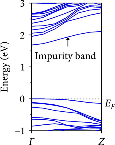
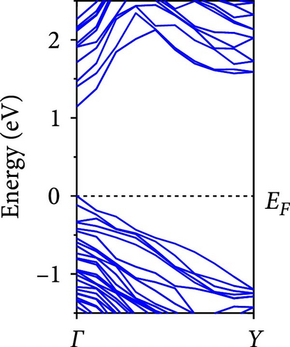
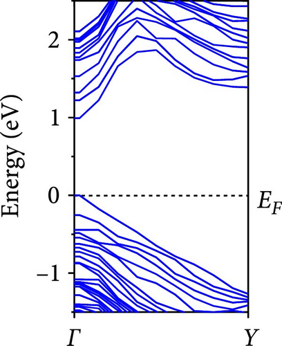
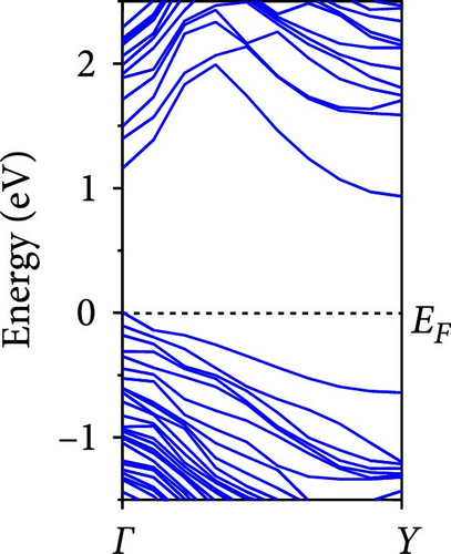
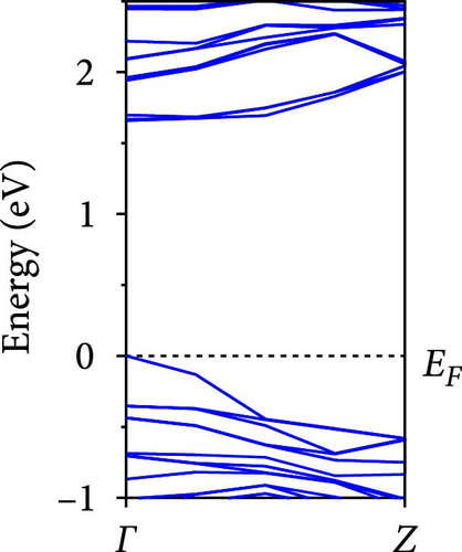
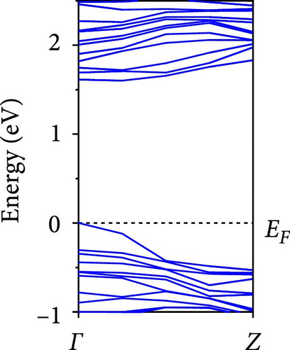
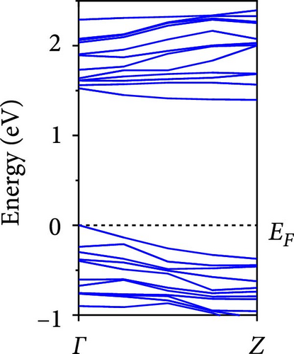
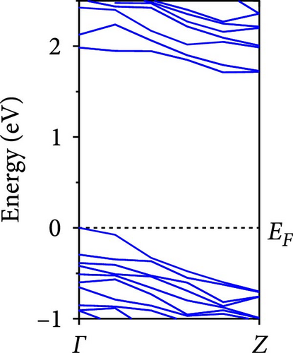
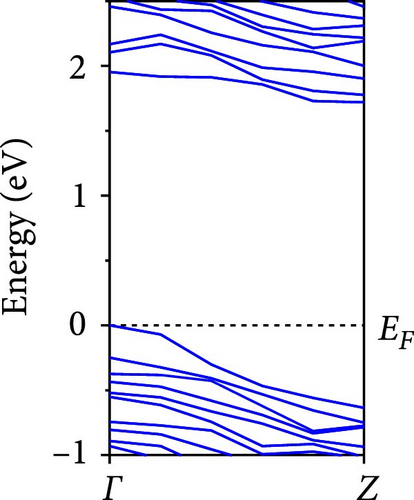
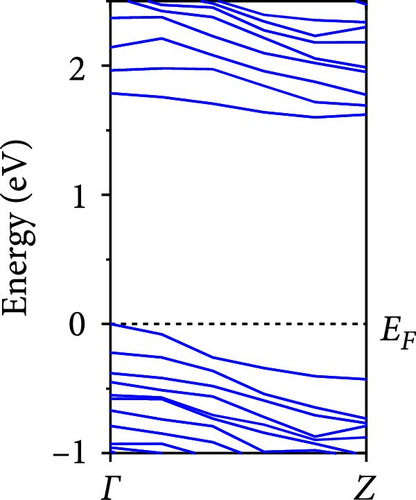
The calculated energy band structures of Si-NWs in four directions are shown in Figures 2, 3, 4, and 5. Before the modification by O atoms, Si [100]-NW, Si [110]-NW, and Si [111]-NW exhibit direct bandgaps with widths of 2.066, 1.144, and 1.659 eV, respectively. After Si-NWs are modified by O atoms in four directions, the formed Si─O─Si bridge bond exhibits small changes in the bandgap, e.g., the bandgap of Si [100]-NWs decreases to 1.922, 1.935, and 1.948 eV, the bandgap of Si [110]-NW decreases to 0.991 eV, the bandgap of Si [111]-NW decreases to 1.601 eV and the bandgap of Si [112]-NW increases from 1.712 to 1.721 eV, respectively. No obvious impurity bands appear on the band edge. However, the Si═O double bond formed by the surface modification yields a more obvious change of bandgap. For example, the bandgaps of Si [100]-NW, Si [110]-NW, Si [111]-NW, and Si [112]-NW decrease to 1.684, 0.931, 1.398, and 1.600 eV, respectively. The obvious impurity bands are observed on the band edges. In addition, after the modification by O atoms, the bandgap characteristics of Si [100]-NW and Si [112]-NW remain unchanged, while the bandgap characteristics of Si [110]-NW forming the Si═O bond and Si [111]-NW change from direct to indirect bandgaps.
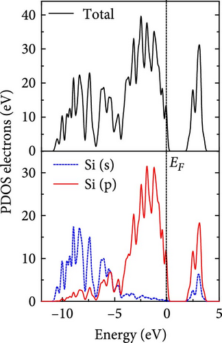
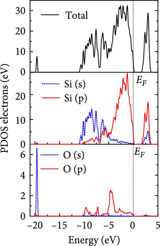
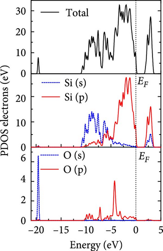
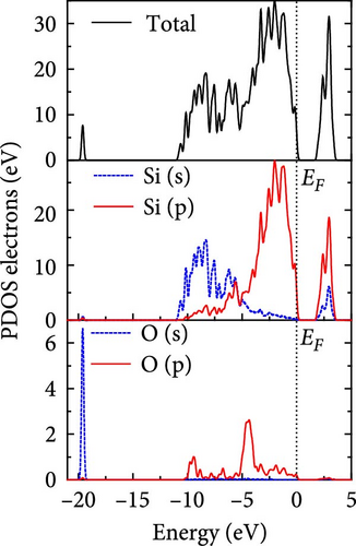
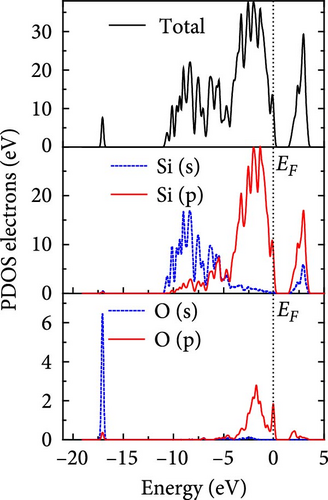
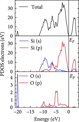
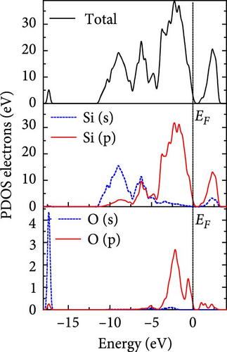
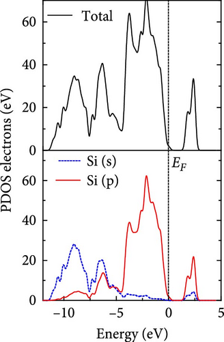
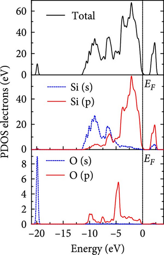
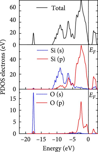
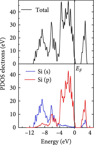
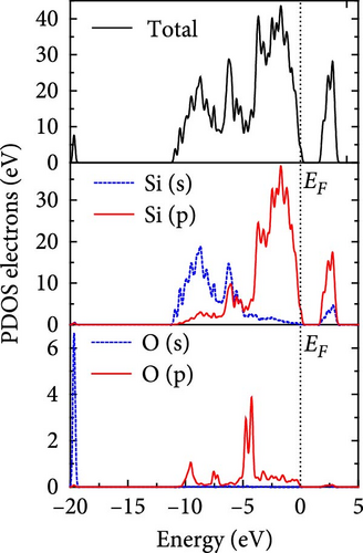
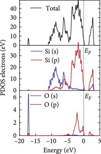
The total density of states and partial density of states of Si-NW in four directions are shown in Figures 6, 7, 8, and 9. The density of states in Figures 6(a), 7(a), 8(a), and 9(a) show that before the modification by O atoms, the conduction bands are mainly contributed by Si3p state electrons, the valence bands consist of upper and lower parts, in which the upper valence bands between at −4 and 0 eV (EF) are mainly contributed by Si3p state electrons, and the lower valence bands between at −12 and −4 eV are mainly contributed by Si3s state electrons [28]. After the modification, the density of states diagrams for Si-NWs forming the Si─O─Si bridging bonds are shown in Figures 6(b), 6(c), 6(d), 7(b), 8(b), and 9(b). The partial density of states contributed by Si atoms is very little affected by modification by O atoms, while the partial density of states contributed by O atoms can be regarded as composed of three parts, in which the upper valence band is mainly contributed by 2 p state electrons of O atoms between−10 and 0 eV and its peak is near −4.5 eV. The lower valence band exhibits a sharp peak in the density of states diagram near −19.5 eV, which is mainly contributed by the 2s state electrons of the O atom, having little contribution to the density of states in the conduction band. Therefore, the energy band of the Si─O─Si bridge bond of Si-NW formed by the oxygen modification undergoes little change at the band edge compared with the unmodified case. The density of states diagrams for Si═O double bonds of Si-NWs are shown in Figures 6(e), 7(c), 8(c), and 9(c), in which the partial density of states contributed by O atoms change greatly. First, the sharp peaks in the density states plot of the lower valence bands formed by the contribution of 2s state electrons of O atoms move from −19.5 to −17.5 eV. Second, both the upper valence bands and the conduction bands exhibit the density of state peaks contributed by the 2p state electrons of the O atoms at the band edges, greatly influencing the Si-NW energy band structure and being more conducive to luminescence. These results are consistent with the existing literature data [16]. Therefore, the surface modification forming the Si═O double bond is apromising approach toward preparing Si-based luminescent nanomaterials.

3.3. Optical Properties
4. Conclusion
In this work, the geometries, electronic structures, and optical properties in four directions of the Si-NWs surface modified by O atoms are systematically studied using the first-principles method based on DFT. The main conclusions can be summarized as follows: (1) After the modification by O atoms, the cell volumes of Si-NWs in four directions become smaller, and the Si─Si bonds in the adjacent oxygen-modified region elongate. In addition, the length of the Si─O─Si bridge bonds is longer than that of the Si═O double bonds. (2) After the modification by O atoms, the energy gaps of Si-NWs become narrower, and impurity bands can be seen in the energy bands; O atoms contribute to the electronic states at the band edge, while the modified Si-NWs form S═O double bonds. In particular, the Si [100]-NW band still exhibits a direct band structure after the modification. (3) a blue shift of ε⊥ components relative to ε‖ can be observed for Si [100]-NW, Si [111]-NW, and Si [112]-NW, and the ε1(ω) and ε2(ω) spectra are red-shifted after Si-NWs is modified by O atoms. Especially, the ε‖ component of Si [100]-NW and the ε(ω) spectra of Si [111]-NWs with the formed Si═O double bond are significantly red-shifted after the modification by O atoms. These results can provide a theoretical reference for preparing nano-silicon and silicon-based optoelectronic devices.
Conflicts of Interest
I hereby declare the following regarding the conflicts of interest involved in this study: This study received funding from Kaili University, with a specific amount of RMB 130,000. This funding is mainly used for purchasing experimental materials, purchasing instruments and equipment, participating in academic conference travel, and printing literature materials. This funding has played a crucial supporting role in the smooth progress of this study, enabling us to obtain necessary experimental equipment and data resources, thereby advancing the depth and breadth of the research. During the research process, we strictly adhere to academic norms and ethical standards to ensure that the interests of sponsors do not affect the objectivity and impartiality of the research results. At the same time, we also conducted a strict review and analysis of the research data to ensure its authenticity and reliability. It should be pointed out that although this study received support from the sponsor, they did not make any inappropriate requests or interventions regarding the specific content, methods, or conclusions of the study. We promise to maintain independence and objectivity in the publication and dissemination of research results without any interference from external interests. In order to maintain the fairness and transparency of academic research, we will clearly indicate the information of the funding sponsor in the relevant research results and publicly disclose all research data and methods for verification and comparison by other researchers. In summary, we are committed to maintaining the independence and impartiality of academic research, ensuring that the support of sponsors does not have any undue impact on research results. We are willing to accept academic supervision and review to ensure the integrity and quality of our research.
Acknowledgments
The study received support from the Special Project of Kaili University (BS201802).
Open Research
Data Availability
The authors confirm that all the relevant data supporting the findings of this study are available within the article.


