Effects of Varying Annealing Ambient towards Performance of Ternary GaxCeyOz Passivation Layers for Metal-Oxide-Semiconductor Capacitor
Abstract
In this work, different annealing ambient (nitrogen-oxygen-nitrogen (N2-O2-N2), forming gas-oxygen-forming gas (FG-O2-FG), and argon-oxygen-argon (Ar-O2-Ar)) were explored to investigate the feasibility of employing the annealed ternary GaxCeyOz passivation layer (PL) for development of Si-based metal-oxide-semiconductor (MOS) capacitors. The impact of nitrogen and/or hydrogen in hindering the growth of silicon dioxide (SiO2) interfacial layer (IL) was quantitatively evaluated. The combination of effects brought by nitrogen attached to oxygen vacancies, nitrogen-silicon bonding, and nitrogen accumulation at the GaxCeyOz/Si interface effectively minimized the formation of SiO2 IL. Consequently, among all the samples, the GaxCeyOz PL annealed in N2-O2-N2 ambient exhibited superior MOS characteristics in terms of low effective oxide charge, slow trap density, interface trap density, and interface state density, which have translated into good leakage current density-electric field characteristics.
1. Introduction
The persistent downscaling of complementary metal-oxide-semiconductor (CMOS) devices, which are the foundation of silicon- (Si-) integrated circuits (IC), serves to enhance device packing density and minimizes power consumption of advanced electronic devices [1]. Consequently, the growing demand of high-performance electronic devices has pushed the scaling of device dimension to its limit, whereby the employment of ultrathin silicon dioxide (SiO2) gate oxide as passivation layer (PL) in Si-based MOS devices would increase the probability of electrons tunnelling through the trapezoidal energy barrier [2]. Inevitably, the occurrence of this direct tunnelling mechanism would promote the undesirable leakage current during the operation of Si-based MOS devices contributing towards the generation of additional heat as well as reliability issues [3]. Therefore, it is necessary to substitute the conventional SiO2 possessing a low dielectric constant (k = 3.9) with a high-k material as PL for Si-based MOS devices [4]. The employment of high-k material would allow the utilization of a physically thicker PL as well as higher gate capacitance for Si-based MOS devices, which would ultimately lead to the accumulation of more charge carriers at the Si channel [5]. Therefore, the utilization of high-k material as a PL in fabricated Si-based MOS devices could potentially result in the ability to simultaneously endure a higher electric breakdown field and a lower leakage current density [5, 6]. To this day, a vast range of high-k substances, such as Al2O3 [7], CeO2 [8], Yb2O3 [9], ZrO2 [10], HfO2 [11], Nd2O3 [12], La2O3 [13], MgO [14], and Tm2O3 [15], have been studied as possible alternatives to SiO2 as the PL for Si-based MOS devices.
Among these investigated high-k materials, CeO2 has leaped into the forefront to replace conventional SiO2 as the PL for Si-based MOS devices due to the intriguing features of CeO2, such as high-k values ranging from 10 to 16 [8, 16], large bandgap ranging from 3.0 to 3.6 eV [8, 17], low interface state density (<1011 cm-2 eV-1) [18], low stress-induced defect formation [19], and low lattice mismatch with the Si substrate [20]. The utilization of a physically thicker, high-k CeO2 PL would effectively reduce the occurrence of leakage current governed by direct tunnelling mechanism that would result in an improvement in the electric breakdown field of the Si-based MOS device with the usage of CeO2 PL [21]. It was proven in previous research that Si-based MOS capacitor with CeO2 PL subjected to a combination of post-nitrous oxide (N2O) plasma treatment and rapid thermal annealing in nitrogen ambient was able to withstand a high electric breakdown field of 24.67 MV/cm [22]. The versatility of CeO2 to be employed in the applications, such as energy storage, catalysts, and electrochemical devices, was due to its reversible transition from oxidation state of Ce4+ to reduction state of Ce3+, but the feasibility of utilizing this characteristic for passivation layer was deemed to be quite challenging [23, 24]. Earlier studies indicated that although CeO2 has shown the potential as a PL for Si-based MOS devices, the issue of partial reducibility of Ce4+ to Ce3+ states remained present as a challenge due to the polaron hopping mechanism that occurred between localized states within the forbidden gap, resulting in an increase in leakage current through the CeO2 PL [25, 26]. The occurrence of this reducibility effect hampering the passivating property of CeO2 PL was due to the formation of oxygen vacancies [16, 27] that would augment the diffusion of oxygen by modifying the valance state of CeO2, as observed in prior studies [26, 28]. Consequently, there was an increase in the growth of the low-k SiO2 IL due to the availability of a larger number of oxygen ions to diffuse to the Si surface [27]. Besides, the formation of oxygen vacancies in the CeO2 PL would also act as a shallow trap that would promote an increase in leakage current density [29, 30].
In order to circumvent the above-mentioned issue, an initial approach of improving the passivating properties of CeO2 was through the doping of tetravalent cations, such as Zr4+ [31], Sn4+ [32], Si4+ [33], Ti4+ [34], and Hf4+ [35] into the CeO2 crystal lattice. Unfortunately, prior studies have revealed that the doping of tetravalent cations into the crystal lattice of CeO2 has reduced the energy required for defect formation, which in turn promoted the creation of additional oxygen vacancies [36, 37]. Thus, the creation of additional deep states within the bandgap of the investigated tetravalent doped CeO2 would contribute to bandgap narrowing as well as promoting leakage current [27, 36, 38]. Consequently, the use of trivalent cations (M3+), such as Mn3+, Gd3+, Sc3+, La3+, Ho3+, Er3+, and Y3+ ions as a dopant for CeO2, has become the focus of research as a lower energy is required to dope the M3+ ions into CeO2 lattice compared to generating oxygen vacancies through CeO2 phase reduction [39, 40]. Although doping of CeO2 by M3+ leads to the emergence of additional oxygen vacancies to maintain electroneutrality, the ability to forge a strong coulombic interaction between the trivalent ions and oxygen vacancies would give rise to the formation of vacancy dopant defect clusters (M3+-Vo) [41, 42]. The generation of M3+-Vo defect pair in CeO2-doped trivalent ions would increase the energy barrier for oxygen migration [43], thereby limiting the accumulation of oxygen ions at the interface. The generation of M3+-Vo defect pair has been found to exhibit a beneficial effect on Sc3+-, Ho3+-, and Er3+-doped CeO2, whereby these M3+ ions would serve as scavengers of oxygen vacancies, inhibiting the diffusion of oxygen ions towards the interface [40, 44]. Moreover, the strength of the interaction between M3+-Vo defect pair was found to be significantly influenced by the ionic radius difference among the trivalent ions and Ce4+ ions, indicating that the doping of trivalent ions having smaller ionic radii could lead to the strengthening of the interaction between these ions and oxygen vacancies, ultimately leading to the inhibition of oxygen diffusion [41].
This study proposes to use trivalent gallium (Ga3+) ions doped into the CeO2 crystal lattice to form a ternary GaxCeyOz, whereby a larger difference in ionic radius between the Ga3+ ion (0.62 Å) [45] and the Ce4+ ion (0.97 Å) [46] would translate to a stronger coulombic interaction between Ga3+ and oxygen vacancies, thereby restricting oxygen ions from diffusing to the interface [47]. Additionally, the passivating properties of the GaxCeyOz PL could be improved due to the excellent properties of Ga2O3, which includes the possession of a larger bandgap of 4.9 eV [48] as well as high-k values (10.2-14.2) [49, 50]. Optimizing the postdeposition annealing parameters is crucial to further improve passivating characteristics of the GaxCeyOz PL, as previous research has revealed that the GaxCeyOz PL annealed at 700°C in a nitrogen-oxygen-nitrogen (N2-O2-N2) ambient has shown the best MOS characteristics in terms of the minimum leakage current density, maximum k value, and the largest bandgap [51]. Moreover, the process of annealing at a temperature of 700°C in N2-O2-N2 ambient was found to be highly effective in regulating the growth of the SiO2 IL [51]. This was due to the existence of nitrogen ions which actively participated in attaching to the oxygen vacancies, thereby hampering oxygen ions from diffusing to the interface [51]. It is worth highlighting that oxygen gas was introduced during dwelling stages regardless of the employment of different gases during the heating and cooling stages with the purpose of repairing the oxygen-related defects and broken bonds [52]. It was proven in other research works that a reduction in interface trap density [53, 54] and fixed oxide charge [55, 56] as well as a low leakage current [57, 58] and negligible hysteresis [59, 60] was reported when the high-k materials acting as PL were subjected to postdeposition annealing in oxygen ambient. Nevertheless, postdeposition annealing in oxygen ambient would result in an exaggeration in the formation of SiO2 IL between the high-k PL and Si substrate [61]. Hence, previous investigation on high-k materials as the PL has diverted towards the usage of nitrogen ambient during postdeposition annealing process for the nitrogen ions to diffuse to the interface between the PL and Si substrate, to accumulate, and to form a barrier layer in order to impede the formation of SiO2 interfacial layer [62]. Moreover, the utilization of ambient comprising of nitrogen and hydrogen gases during postdeposition annealing would facilitate the reduction of defect states and the improvement of interface quality by passivating the Si dangling bonds with either the hydrogen or the nitrogen, as well as by having the nitrogen to attach to oxygen vacancies, which would eventually improve leakage current density and breakdown field of the Si-based MOS devices [63, 64]. Besides nitrogen and hydrogen gases, the beneficial effects of utilizing argon ambient during postdeposition annealing were also being highlighted for other high-k PL, wherein an improvement in leakage current density, interface trap density, and effective oxide charge, as well as the mitigation in the formation of SiO2 interfacial layer, was reported when argon ambient was being used [65, 66]. Dissimilar from previous work, this work intends to utilize different combinations of gases during postdeposition annealing process, whereby different gases will be used during the heating and cooling stages while oxygen gas will be kept the same during the dwelling stage of the postdeposition annealing process. Hence, a combination of forming gas-oxygen-forming gas (FG-O2-FG), nitrogen-oxygen-nitrogen (N2-O2-N2) [51], and argon-oxygen-argon (Ar-O2-Ar) at 700°C was used to provide a comparative study on the structural, morphological, optical, and metal-oxide-semiconductor (MOS) characteristics of GaxCeyOz PL deposited on Si substrate, which has not been reported in previous works.
2. Experimental
The 4-inch n-type Si substrate (100) orientation was sliced into 1 cm2 dimension and subjected to standard Radio Corporation of America (RCA) cleaning process. Following that, the RCA cleaned samples were immersed in a diluted hydrofluoric (HF) acid solution to etch the native oxide of SiO2 from the surface of Si substrate. It was highlighted in previous research works on the importance of chemical purity in the formation of a high-quality passivation layer, wherein all chemicals being used in this work are having a purity level of 99.99% [67, 68]. Initially, 0.191 g of gallium(III) nitrate hydrate (Sigma-Aldrich, 99.99%) was dissolved in 5 ml of methanol (J.T. Baker, analytical grade) and stirred for 15 min at 30°C on a hot plate to form a 0.25 M gallium-containing precursor. Subsequently, 1.0936 g of cerium(III) acetylacetonate hydrate (Sigma-Aldrich, 99.99%) was dissolved in 3 ml of methanol (J.T. Baker, analytical grade) and 6 ml of acetic acid (J.T. Baker, CMOS grade) and stirred for 15 min at 60°C to prepare a 0.25 M cerium-containing precursor. Finally, the cerium- and gallium-containing precursors were stirred continuously for 30 min at 60°C to obtain a ratio of 1 : 1. Then, the resulting GaxCeyOz precursor was cooled down to room temperature. Subsequently, the GaxCeyOz precursor was spin-coated on an RCA-clean n-type Si substrate with an rpm of 3000 for 30 s. These as-deposited samples were subjected to postdeposition annealing in different ambient of FG-O2-FG, N2-O2-N2, and Ar-O2-Ar for 30 min at 700°C in a quartz tube furnace. During the heating and cooling stages, FG or N2 or Ar (100 ml/min) was flown into the furnace while O2 gas with a similar flow rate was employed during the dwelling stage. After completing the postdeposition annealing process, the Al/GaxCeyOz/Si/Al MOS capacitors were realised by evaporating aluminium (Al) contact on the surface of the GaxCeyOz PL using a shadow mask (diameter = 0.2 mm) and a layer of Al was deposited as the back contact on Si substrate.
Crystalline phase and orientation of the investigated GaxCeyOz PL subjected to different postdeposition annealing ambient were characterized using grazing incident X-ray diffraction (GIXRD; Bruker D8 Discover) analysis. The surface morphologies and cross sectional images, as well as elemental composition of the investigated GaxCeyOz PL, were carried out using field-emission scanning electron microscopy (FESEM; FEI Nova NanoSEM 450) equipped with energy dispersive X-ray analysis (EDX; JSM-6460 LV). The estimation of thickness for the GaxCeyOz PL and SiO2 IL was determined based on the acquired X-ray reflectivity (XRR) results measured using Bruker D8 Discover. 3-dimensional topographies as well as root-mean-square (RMS) roughness of the investigated GaxCeyOz PL were characterized using atomic force microscopy (AFM; Dimension Edge, Bruker). The bandgap of investigated GaxCeyOz PL was extracted from diffused reflectance spectra acquired using ultraviolet–visible (UVVIS) spectrophotometer (Cary 5000). The capacitance-voltage (C-V) and current-voltage (I-V) characteristics of the investigated samples were measured using Keithley 4200-SCS parameter analyzer.
3. Results and Discussions
3.1. Structural, Chemical, and Optical Characteristics of GaxCeyOz PL Annealed in FG-O2-FG, N2-O2-N2, and Ar-O2-Ar Ambient
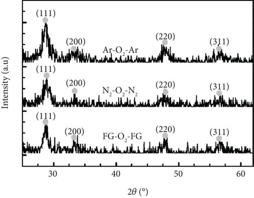
The GIXRD pattern as represented in Figure 1 indicates that the GaxCeyOz PL annealed in FG-O2-FG, N2-O2-N2, and Ar-O2-Ar ambient at 700°C have emerged as polycrystalline, with the detection of GaxCeyOz phase oriented in (111), (200), (220), and (311) planes for all of the GaxCeyOz PL, which were indexed with the International Centre for Diffraction Data (ICDD) file no. 00-034-0394 for cubic fluorite CeO2 phase. Additionally, it was also perceived that no additional phases with regard to either cubic Ga2O3 (ICDD file no. 00-020-0426) or monoclinic Ga2O3 (ICDD file no. 00-041-1103) phases were detected from the attained GIXRD results indicating that no phase separation has taken place. Furthermore, it was observed that the GIXRD peaks associated with the GaxCeyOz phase exhibited a displacement towards a higher diffraction angle in contrast to the CeO2 phase documented in the ICDD file no. 00-034-0394. This could be an indication that Ga3+ ions having a smaller ionic radius of 0.62 Å than Ce4+ ions (0.97 Å) have successfully doped into the CeO2 crystal framework to form ternary GaxCeyOz phase.
| Annealing ambient | Lattice parameter a (nm) | Crystallite size D (nm) | Microstrain ε |
|---|---|---|---|
| N2-O2-N2 | 0.5350 | 15.92 | 0.0072 |
| FG-O2-FG | 0.5380 | 13.87 | 0.0057 |
| Ar-O2-Ar | 0.5387 | 19.99 | 0.0109 |
| Standard CeO2 | 0.5411 | — | — |
Further scrutiny was conducted through the utilization of EDX analysis on the scrutinized GaxCeyOz PL, and the resulting findings are subsequently depicted in Table 2. It was perceived that the sample annealed in FG-O2-FG ambient attained a higher atomic percentage (at%) of nitrogen when compared to N2-O2-N2 ambient although the employment of forming gas ambient was contained of a lower proportion of nitrogen (90%) in contrast to pure nitrogen ambient. The aforementioned observation has served to bolster the prior postulation that the utilization of FG-O2-FG ambient would incite the initial attachment of hydrogen ions to the oxygen vacancies, owing to the superior diffusion rate of hydrogen ions as compared to nitrogen ions. Since the ionic radius of hydrogen ions was smaller than that of nitrogen ions, the attachment of hydrogen ions to the oxygen vacancies would provide sufficient space in the lattice for the passage of the nitrogen ions to the interface between the GaxCeyOz PL and Si substrate when compared with the attachment of nitrogen ions to the oxygen vacancies. Consequently, the outcome of the postdeposition annealing process in FG-O2-FG ambient was the buildup of a higher concentrations of nitrogen ions at the interface to act as a more potent oxygen diffusion barrier layer, which is highly effective in hindering the formation of SiO2 IL. The lower value of at% of nitrogen in the GaxCeyOz PL annealed in N2-O2-N2 ambient could be due to the higher likelihood of nitrogen ions attaching to the oxygen vacancies, wherein narrower spacing within the GaxCeyOz lattice would impede the nitrogen ions from diffusing towards the interface. This indicates that the initially inward diffusing nitrogen ions that were unable to form attachment with oxygen vacancies or diffuse to the interface between GaxCeyOz PL and Si substrate would subsequently diffuse out of the PL aiding in the acquisition of a lower at% of nitrogen during annealing in N2-O2-N2 ambient. It was noticed that the acquisition of a higher at% of oxygen for GaxCeyOz PL annealed in FG-O2-FG ambient when compared with N2-O2-N2 ambient has further reinforced that the simultaneous attachment of hydrogen and nitrogen ions with oxygen vacancies has minimized the release of oxygen ions from GaxCeyOz lattice. Nevertheless, it was perceived that Ar-O2-Ar ambient has led to the attainment of the minimum at% of oxygen in GaxCeyOz PL, but it did not necessarily translate into large amount of oxygen vacancies as evidenced by the close lattice parameter a between CeO2 and GaxCeyOz.
| Annealing ambient | O (at. %) | Ce (at. %) | Ga (at. %) | N (at. %) |
|---|---|---|---|---|
| N2-O2-N2 | 69.45 | 16.89 | 9.80 | 3.85 |
| FG-O2-FG | 69.84 | 16.09 | 9.43 | 4.64 |
| Ar-O2-Ar | 64.92 | 24.34 | 10.73 | — |
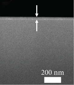
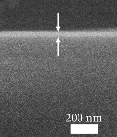
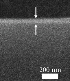
The FESEM images of the examined GaxCeyOz PL shown in Figure 2 could be utilized to analyze the effectiveness of nitrogen and/or hydrogen ions in hindering the formation of SiO2 IL. The total oxide thickness of the investigated PL was calculated from 10 distinct points, as illustrated in Table 3. It was deduced that the existence of nitrogen and/or hydrogen ions was effective in minimizing the formation of SiO2 IL as the average total oxide thickness obtained by both GaxCeyOz PL subjected to postdeposition annealing in N2-O2-N2 (30.41 nm) and FG-O2-FG ambient (40.16 nm) was lower than that of Ar-O2-Ar (53.75 nm). In addition, it was also divulged that FG-O2-FG ambient was not as effective as N2-O2-N2 ambient in retarding the diffusion of oxygen ions to react with Si surface as a larger average total oxide thickness was attained by the GaxCeyOz PL annealed in FG-O2-FG ambient. The proposition being put forward posited that the accumulation of hydrogen ions at the interface may be comparatively inadequate in impeding the diffusion of oxygen ions towards the interface, in contrast to the accumulation of nitrogen ions at the same interface. It was hypothesised that the accumulation of hydrogen ions with a smaller ionic radius at the interface and a weaker bond strength between the hydrogen ions and Si [68] would enable the oxygen ions to either bypass or disrupt these bonds, leading to the reaction with the underlying Si surface during annealing in FG-O2-FG ambient. This reaction would contribute to the development of a thicker SiO2 IL in comparison to N2-O2-N2 ambient.
| Annealing ambient | XRR: GaxCeyOz PL thickness (nm) | XRR: SiO2 IL thickness (nm) | XRR: total oxide thickness (nm) | Cross-sectional FESEM: total oxide thickness (nm) | k value |
|---|---|---|---|---|---|
| N2-O2-N2 | 28.054 [51] | 0.958 [51] | 29.012 [51] | 30.4 | 11.27 [51] |
| FG-O2-FG | 36.240 | 2.321 | 38.561 | 40.2 | 18.24 |
| Ar-O2-Ar | 45.112 | 6.942 | 52.054 | 53.7 | 15.94 |
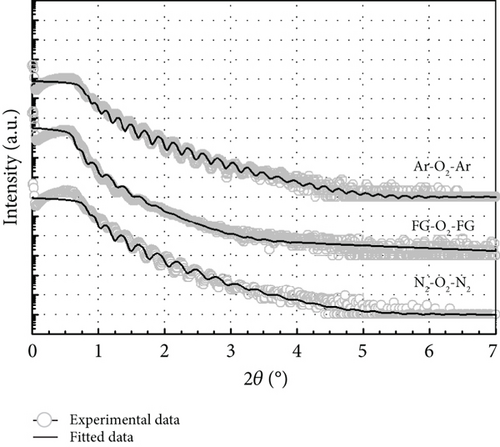
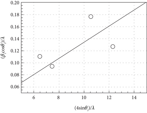

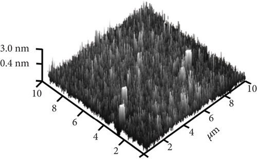
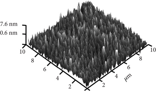
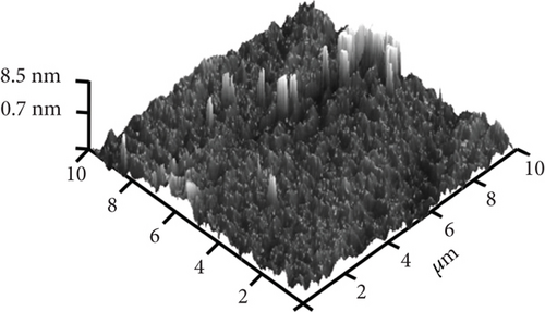
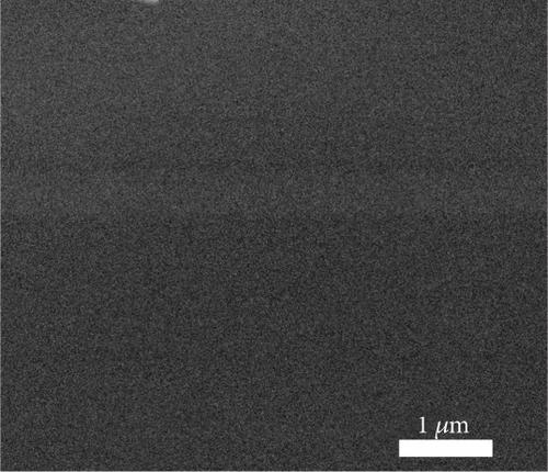
The typical surface morphology of GaxCeyOz PL annealed in Ar-O2-Ar ambient that was characterized using FESEM technique is shown in Figure 7(d). It was revealed that all of the investigated GaxCeyOz PL have acquired a smooth surface without visible cracks or voids. Additional assessment was conducted utilizing the AFM characterization, whereby the 3-dimensional surface topographies of the GaxCeyOz PL were acquired at a scanning area of 10 μm2 as presented in Figure 7. It was observed that smaller dimension protrusions with comparable height were uniformly formed throughout the surface of GaxCeyOz PL annealed in a N2-O2-N2 ambient (Figure 7(a)) leading to the attainment of the lowest root-mean-square (RMS) roughness of 0.793 nm. A substantial increment in RMS roughness to 2.080 nm was noticed when the GaxCeyOz PL was annealed in FG-O2-FG ambient, wherein a mixture of protrusions with large and small dimensions was formed throughout the surface of this PL (Figure 7(b)). It was observed that the surface of GaxCeyOz PL annealed in Ar-O2-Ar ambient was comprised of a section with extremely larger protrusion (Figure 7(c)), and thus, the highest RMS roughness of 2.580 nm was attained.
3.2. The Metal-Oxide-Semiconductor (MOS) Characteristics of the Al/GaxCeyOz/4H-SiC/Al MOS Capacitor
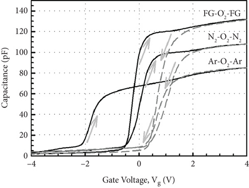
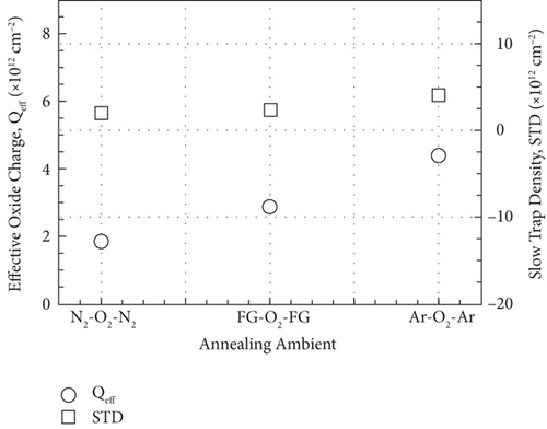
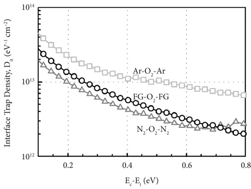
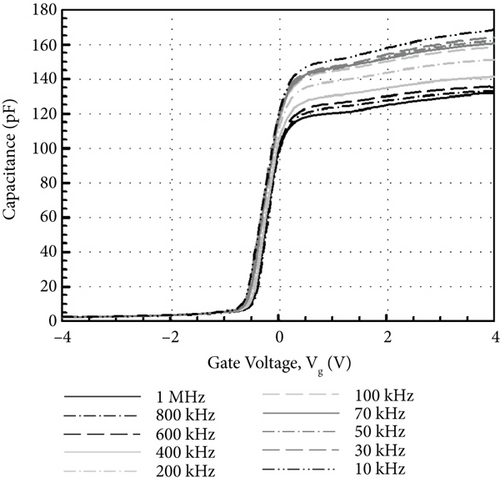

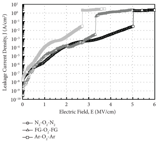
Figure 13 illustrates the leakage current density-electric field (J- E) characteristics of the GaxCeyOz PL annealed at 700°C in different ambient. At E below 0.5 MV/cm, GaxCeyOz PL annealed in FG-O2-FG ambient has demonstrated a lower J due to the existence of a higher concentration of border traps located at a lower trap energy level in which high-low-frequency C-V measurement has revealed the acquisition of a lower Nss at gate voltage below 0.05 V. A deterioration in J was perceived as the E was enhanced to the region of 0.5 to 2.0 MV/cm for the GaxCeyOz PL annealed in FG-O2-FG ambient, which was due to the presence of a higher density of border traps at a higher gate voltage of 0.05 V as well as a higher Dit. Nonetheless, a sudden improvement in J at E within the region of 2.0 to 3.0 MV/cm for the GaxCeyOz PL annealed in FG-O2-FG ambient was due to the formation of thicker SiO2 IL and the highest k value when compared with GaxCeyOz PL annealed in N2-O2-N2 ambient. Although GaxCeyOz PL annealed in N2-O2-N2 ambient has attained the lowest k value, this PL was able to withstand the highest electric breakdown field of ~4.95 MV/cm that could be potentially due to the acquisition of the lowest Qeff, STD, and Dit. It was revealed that the acquired electric breakdown field (EB) of 4.95 MV/cm for the GaxCeyOz PL annealed in N2-O2-N2 ambient was better when compared with EB of bilayer HfO2/SiO2 (3.90 MV/cm) PL [92]. Moreover, the attained leakage current density of 2.57 × 10⁻⁶ A/cm-2 at 1 MV/cm for the GaxCeyOz PL annealed in N2-O2-N2 ambient was lower than the magnetron sputtered ErAlO PL on Si substrate (8.40 × 10⁻⁵ A/cm2 at 1 MV/cm) [80]. It was discerned that GaxCeyOz PL annealed in Ar-O2-Ar ambient has demonstrated the lowest electric breakdown field (~2.71 MV/cm) due to the formation of the thickest SiO2 IL as well as the less dense GaxCeyOz PL, resulting in a poor J- E characteristic. It was postulated that the formation of the thickest SiO2 IL during annealing in Ar-O2-Ar ambient would assist in enhancing the electric breakdown field of this PL with the requirement that a high-quality SiO2 IL was formed. However, the attainment of the poorest J- E characteristic by this GaxCeyOz PL annealed in Ar-O2-Ar ambient has suggested that a low quality of SiO2 IL was formed contributing to a degradation in EB of this PL.
4. Conclusion
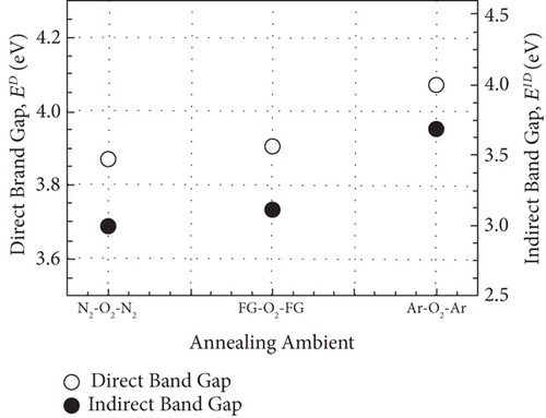
A comparison study among GaxCeyOz PL annealed in different ambient (N2-O2-N2, FG-O2-FG, and Ar-O2-Ar) was carried out systematically. Hydrogen present in the FG-O2-FG ambient would attach to oxygen vacancies in the GaxCeyOz PL, stimulating diffusion of nitrogen from the ambient to the GaxCeyOz/Si interface. Effectiveness of nitrogen and/or hydrogen in reducing the formation of SiO2 IL was reported. The extracted ED and EID values (3.87 to 4.07 and 2.99 to 3.68 eV, respectively) were within the range of reported values for CeO2 and Ga2O3, which further reinstated the formation of the ternary GaxCeyOz phase. The GaxCeyOz PL annealed in FG-O2-FG ambient possessed the largest k value of 18.24, followed by the samples annealed Ar-O2-Ar (15.94) and N2-O2-N2 (11.27) ambient. It was revealed that N2-O2-N2 ambient was effective in passivating Si dangling bonds and oxygen vacancies in addition to the accumulation of nitrogen at the interface, which resulted in the acquisition of a lower Dit, Qeff, and STD. However, a higher concentration of unattached nitrogen in the GaxCeyOz PL annealed in FG-O2-FG has degraded the interface quality when compared with the sample annealed in N2-O2-N2 ambient. Moreover, annealing in Ar-O2-Ar ambient has led to the acquisition of the lowest EB (2.71 MV/cm) due to the attainment of the highest Qeff, STD, Dit, and Nss. Hence, it was perceived that a low quality of SiO2 IL was formed during annealing in Ar-O2-Ar ambient contributing to the attainment of the lowest EB. Although the GaxCeyOz PL annealed in N2-O2-N2 ambient has a lower k value than other samples, the acquisition of a high EB of 4.95 MV/cm could be associated to the acquisition of low Qeff, STD, Nss, and Dit, which have supported its compatibility as a potential candidate as a high-k PL for future Si-based MOS applications.
Conflicts of Interest
The authors declare that they have no conflicts of interest.
Acknowledgments
The authors would like to acknowledge the financial support from the Ministry of Higher Education Malaysia for Fundamental Research Grant Scheme (FRGS) with Project Code FRGS/1/2023/STG05/USM/02/8.
Open Research
Data Availability
The raw/processed data required to reproduce these findings cannot be shared at this time as the data also forms part of an ongoing study.


