Nanomaterials in Nanophotonics Structure for Performing All-Optical 2 × 1 Multiplexer Based on Elliptical IMI-Plasmonic Waveguides
Abstract
In this study, an all-optical multiplexer (Mux) based on elliptical insulator-metal-insulator (IMI) plasmonic waveguides is designed. The area of the proposed structure is very small (400 nm × 400 nm) which operates at a wavelength of 1,550 nm. The developed device utilizes constructive and destructive interferences between the input signals and the selector signal. This structure is less complex and has lower loss compared to the previous works. Transmission (T), contrast ratio (CR), modulation depth (MD), insertion loss (IL), and contrast loss (CL) are the five parameters that describe the performance of the plasmonic Mux. The transmission threshold between logic 0 and logic 1 is 0.5. Moreover, the maximum transmission efficiency of the device is 163%. Moreover, based on the MD value of 95.09%, the dimensions of the proposed structure are excellent and optimal. The proposed plasmonic Mux structure contributes substantially to developing an all-optical arithmetic logic unit (ALU) and all-optical signal processing nanocircuits. The finite element method (FEM) simulates the proposed plasmonic multiplexer with COMSOL Multiphysics 5.4 software.
1. Introduction
Nowadays, optical devices based on surface plasmon polaritons (SPPs) are of interest to researchers in integrated circuit design [1]. SPPs are the surface electromagnetic waves that propagate along metal-dielectric interfaces and arise from the interaction between the electromagnetic waves and the free electrons of metals [1]. The ability to fabricate low-loss devices with dimensions of less than 100 nm and to confine the light beyond the diffraction limit led to designing all-optical SPP structures [2]. The basic idea for creating plasmonic devices is to control the destructive and constructive interferences between light signals in plasmonic waveguides [3–5]. In recent years, many passive and active SPP devices have been designed, such as switches [6, 7], logic gates [8–15], sensors [16–18], nanowires [19, 20], splitters [21], filters [22, 23], couplers [24], resonators [25], multiplexers, and demultiplexers [26–29]. There are two main types of plasmonic waveguides used in this way: MIM and IMI plasmonic waveguides. In IMI waveguides, the propagation length is longer, the propagation loss is lower, and it has a more straightforward fabrication process [8].
Other important applications and research studies are mentioned in this section. A numerical investigation of an all-optical SR flip-flop using plasmonic metal-insulator-metal (MIM) waveguides at the wavelength of 1,550 nm has been discussed in reference [30]. This research attempts to understand the behavior and performance of this device in optical signal processing applications. The study focuses on how the device operates and how the plasmonic properties can be utilized to achieve high-speed and low-power operation. The creation of an all-optical signal router utilizing plasmonic waveguides is covered in reference [31]. The main objective of this study is to suggest an effective and small architecture for an optical signal router that can control and route optical signals in communication networks. The authors aim to achieve improved performance, such as low-signal loss, high-speed operation, and smaller device footprint, by exploiting the special characteristics of plasmonic waveguides.
As for the most important previous works on the multiplexer, a 2 × 1 all-optical multiplexer with a threshold limit of 0.5 using a Kerr nonlinear nanoplasmonic switch, was used as discussed in reference [28]. This structure operates at 685 nm and 793.2 nm wavelengths. However, the size of this structure is relatively large, equal to 3000 nm × 2400 nm, and its fabrication will be complex. Furthermore, the optimal transmission efficiency of this Mux is 70%. A broadband mode converter and multiplexer based on dielectric-loaded plasmonic waveguides were discovered in reference [29]. This structure operates at a 1,550 nm wavelength, and the maximum transmission at this wavelength is low. In addition, this structure is relatively large and its construction will be complicated.
The plasmonic multiplexer based on nanogroove arrays with two operational wavelengths was designed in reference [32]. This structure operates at 650 nm and 850 nm wavelengths. However, the size of this structure is relatively large, which is equal to 7.5 μm × 6 μm, and its fabrication will be complex. In addition, the transmission threshold between logic 0 and logic 1 is less than 0.5. An all-optical 2 × 1 multiplexer using an MIM-based plasmonic waveguide has been proposed in reference [33]. This structure has a transmission threshold of 0.5 between the logic 0 and logic 1. However, its size is relatively large at 9.2 μm × 7.8 μm, and its production will be harrowing due to the complexity of its design.
This study proposes a structure of three straight waveguides coupled to two elliptical IMI-plasmonic waveguides to realize a 2 × 1 multiplexer with a high-transmission ratio. The designed structure has a minimum size of 400 nm × 400 nm, and the operating wavelength is 1,550 nm. The numerical results are obtained by FEM using COMSOL Multiphysics 5.4 software. The proposed plasmonic multiplexer can be used in the construction of an all-optical arithmetic logic unit (ALU) and all-optical signal processing nanocircuits. Section 2 describes the resonator selection, configuration, and parameters for the proposed design at 1,550 nm wavelength. Section 3 presents the proposed structure arrangement and theoretical idea of operation. The efficiency of the suggested structure and simulation results are detailed in Section 4. In Section 5, a comparison between the proposed designed structure and previous investigations is provided. In the last section, the main findings of the study are described.
2. Resonator, Structural Type, and Suggested Design Parameter Selection for 1,550 nm Wavelength
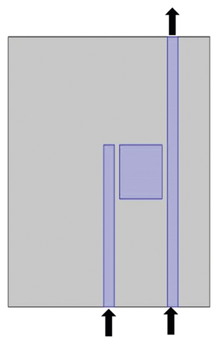
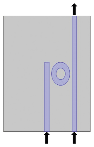
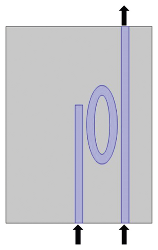
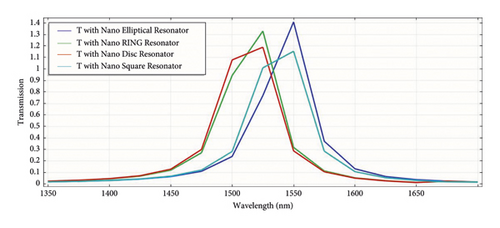
As a starting point for our study, the first structure was created, as shown in Figure 1(a), to build the Mux and to obtain the highest transmission at a wavelength of 1,550 nm. Two strips and a nanosquare resonator make up this suggestion, and the transmission result for this case is shown in Figure 2. Figures 1(b) and 2 illustrate what happened when we changed the geometry of the resonator from a nanosquare to a nanodisc. As depicted in Figure 1(c), we replaced the nanodisc resonator with a nanoring resonator, improving the transmission performance. Finally, the maximum transmission was achieved at 1,550 nm after replacing the resonator with a nanoelliptical resonator, as shown in Figures 1(d) and 2. Therefore, the nanoelliptical resonator is the optimal selection for the given structure. Moreover, the dimensions of the four structures in Figure 1 are detailed in Table 1.

| Parameter with description | Value (nm) |
|---|---|
| Height and width of all structures | 400 |
| Length of middle strips | 240 |
| Length and width of the nanosquare resonator | 80 |
| Largest and smallest major axis of nanoelliptical resonator | 80, 60 |
| Largest and smallest minor axis of nanoelliptical resonator | 40, 20 |
| Radius of nanodisc resonator | 40 |
| Largest and smallest radius of nanoring resonator | 40, 20 |
| Width of stripes | 20 |
| Distance between stripes and all resonators | 10 |
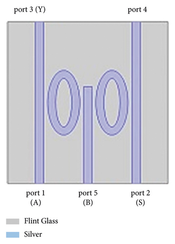
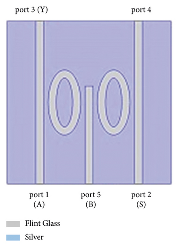
In addition to the need for more than three ports to design Mux, a resonator and a stripe are added as shown in Figure 3. Choosing the type of multilayer (IMI or MIM) plasmonic waveguides, as shown in Figures 3(a) and 3(b), is also one of the most important design considerations. As previously mentioned, there are two common types of plasmonic waveguides which are the insulator-metal-insulator (IMI) waveguide as depicted in Figure 3(a) and the metal-insulator-metal (MIM) waveguide as depicted in Figure 3(b). The differences between these two waveguides are summarized in Table 2 [5, 8, 34, 35]:
| IMI waveguides | MIM waveguides | |
|---|---|---|
| Layer configuration | Dielectric-metal-dielectric | Metal-dielectric-metal |
| Field confinement | Less | More |
| Propagation length | More | Less |
| Propagation loss | Low | Moderate to high |
| Dispersion | Can be engineered | Less control |
| Integration | On-chip integration | Limited integration options |
| Fabrication | Easy | Not easy |
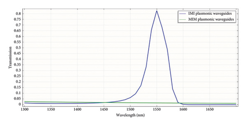
As mentioned in Table 2, for low propagation losses and other advantages and as depicted in Figure 4, the best possible plasmonic waveguide for the proposed design is IMI, with maximum transmission occurring at 1,550 nm wavelength.
The transmission spectrum of the proposed structure is minimized or shifted depending on the structural size, shape, parameters, material’s refractive index, port position, and incident field polarization and phase. In this section, structural parameters are used in validation. The major and minor ellipse axes, a and b, waveguides width, w, the distances between the elliptical waveguides and the stripes, d, and the length of the middle strip, Lms, are considered as structural parameters in validation.
The effect of changing the minor ellipse axis, b, on the transmission coefficient is shown in Figure 5. The transmission spectra are obtained by considering S (port 2) and B (port 5) ports are ON and A port (port 1) is OFF.
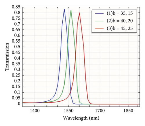
For the largest and smallest minor axis values, three following cases are assumed: (1) 35 nm and 15 nm, (2) 40 nm and 20 nm, and (3) 45 nm and 25 nm. When the width of the waveguide is 20 nm, the largest and the smallest major axes are 80 nm and 60 nm, respectively. Moreover, the middle stripe length and the distances between the elliptical waveguides and stripes are 240 nm and 10 nm, respectively. As shown in Figure 5, the resonance wavelength has a red shift by increasing the largest and smallest values of the minor axis, b; according to the results, when the largest minor axis is 40 nm, and the smallest minor axis value is assumed to be 20 nm, the resonance occurs in the desired wavelength. Therefore, we choose 40 and 20 nm as the largest and smallest values of the minor axis.
The result of changing the major axis on the transmission spectrum is shown in Figures 6(a) and 6(b). Assuming all other parameters remain unchanged, where the waveguide width is 20 nm, and the largest and the smallest minor axes are 40 nm and 20 nm, respectively. It is also assumed that the middle stripe length and the distances between the elliptical waveguides and the stripes are 240 nm and 10 nm, respectively.
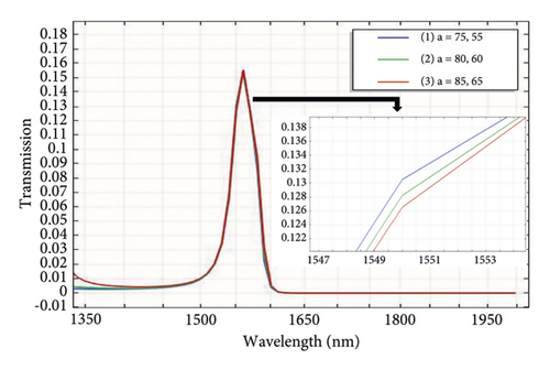
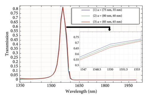
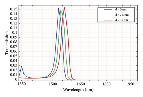
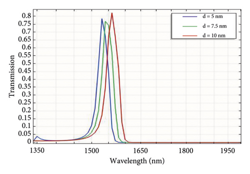
In addition, in case the S port and the input ports are OFF, the transmission is shown in Figure 6(a) by considering three cases for the largest and smallest major axis, a, as follows: (1) 75 nm and 55 nm, (2) 80 nm and 60 nm, and (3) 85 nm and 65 nm. Figure 6(b) shows the transmission of the structure with three values for the largest and smallest major axes, a, in the case of S port and B port are ON, and the A port is OFF.
To achieve the desired result in operational wavelength and to obtain the best contrast ratio, we chose 80 nm for the largest major axis “a” of the ellipse and 60 nm for the smallest.
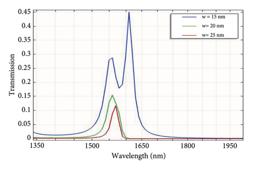
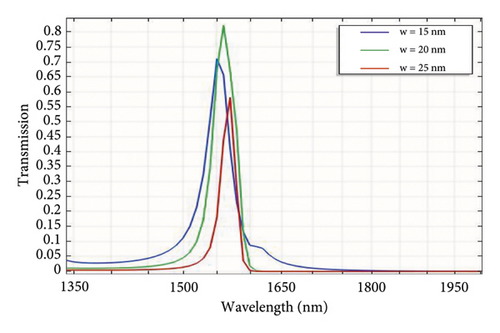
By choosing the desired ellipse’s structural parameters and the distances between the elliptical waveguides and stripes of 10 nm and middle stripe length of 240 nm, the transmission spectrum for three values of w, 15 nm, 20 nm, and 25 nm, is illustrated in Figures 6(c) and 6(d). In Figure 6(c), the case of the S port and input ports are OFF. Figure 6(d) shows the transmission of the S port when the B port is ON and A port is OFF. The width of the waveguide is considered to be 20 nm to obtain the best contrast ratio.
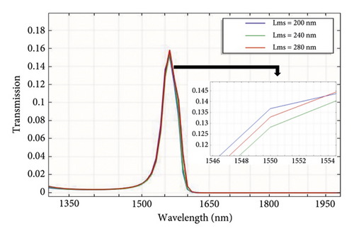
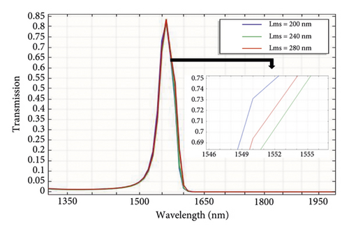
The transmission spectrum for three values of the distance between the elliptical waveguides and the stripes, 5, 7.5, and 10 nm, with proper structural dimensions and middle stripe length, is shown in Figures 6(e) and 6(f). The transmission spectrum shown in Figure 6(e) relates to the S port and input ports being OFF. Figure 6(f) shows the transmission when the S port and B port are ON and the A port is OFF; according to the results for getting the best contrast ratio in Figures 6(e) and 6(f), we chose 10 nm for the distance between the elliptical waveguide and the stripes. Finally, by assuming the obtained structural parameters, the effect of changing the middle stripe length on the transmission spectrum is illustrated in Figures 6(g) and 6(h). Figure 6(g) shows the transmission when the S and input ports are OFF. In addition, the transmission spectrum in the case of the S port and B port is ON, and the A port is OFF, as shown in Figure 6(h). According to the results, the middle stripe length is chosen as 240 nm to achieve the best contrast ratio. All of the cases studied mentioned in Figure 6 are listed in Table 3.
| Dimensions | Dimension length (nm) | (Pout |OFF) | (Pout |ON) | Contrast ratio | Best dimension (nm) |
|---|---|---|---|---|---|
| Largest, smallest major axis “a” | 75, 55 | 0.13 | 0.69 | 7.24 | 80, 60 |
| 80, 60 | 0.127 | 0.675 | 7.25 | ||
| 85, 65 | 0.125 | 0.66 | 7.22 | ||
| Stripes width “w” | 15 | 0.28 | 0.71 | 4.04 | 20 |
| 20 | 0.127 | 0.675 | 7.25 | ||
| 25 | 0.037 | 0.18 | Fault | ||
| Distances between the elliptical waveguides and stripes “d” | 5 | 0.09 | 0.44 | Fault | 10 |
| 7.5 | 0.142 | 0.741 | 7.17 | ||
| 10 | 0.127 | 0.675 | 7.25 | ||
| Middle stripe “Lms” | 200 | 0.138 | 0.73 | 7.23 | 240 |
| 240 | 0.127 | 0.675 | 7.25 | ||
| 280 | 0.133 | 0.695 | 7.1 | ||
3. Structure Layout
Based on the previous sections and the shape and dimensions selected, the proposed 2 × 1 Mux based on IMI-plasmonic waveguide consisting of two elliptical waveguides and three straight stripes, as shown in Figures 7(a) and 7(b), has been proposed. The metal region is silver, and the insulator medium is realized by flint glass (pure), and the substrate is made of a semiconductor material such as silicon in the case of the used three-dimensional (3D) structure. The permittivity of silver is characterized by the findings of Johnson and Christy [36], and the refractive index of the flint glass is 1.61 [37]. The design area of the proposed architecture is 400 nm × 400 nm. Moreover, the lengths of the two side stripes are 400 nm, and Table 4 details the length of the middle stripe Lms and all dimensions of the proposed structure. The operating wavelength is 1,550 nm, the best choice for optical communication applications.
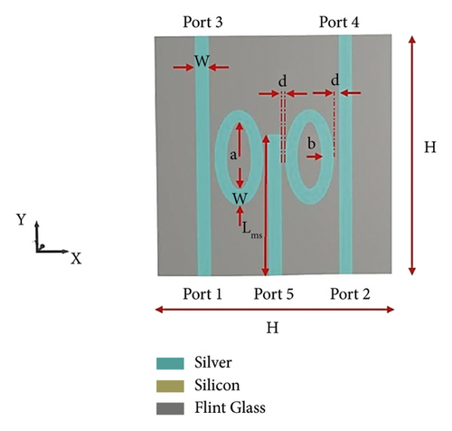
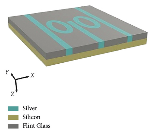
| Parameter | Description | Value (nm) |
|---|---|---|
| H | Height and width of the structure | 400 |
| Lms | Length of middle stripe | 240 |
| a | Largest and smallest major axis “a” | 80, 60 |
| b | Largest and smallest minor axis “b” | 40, 20 |
| W | Width of stripes and nanoellipse resonator | 20 |
| d | Distance between stripes and nanoellipse resonator | 10 |
The two-dimensional (2D) FEM technique is used to solve the Maxwell equations numerically, and a convolutional perfectly matched layer (CPML) is considered to absorb the boundary condition of the simulation domain. A transverse magnetic (TM)-polarized plane wave with Ex, Ey, and Hz, electromagnetic field components, excites the structure. The designed Mux has five ports as follows: ports 1 and 5 are input ports, port 2 is considered as selector port, port 3 is the output port, and port 4 is always ON. The other details of the input source parameters in the software used are given in Table 5.
| Input source parameters | Description or values |
|---|---|
| Input power | 1 μw |
| Software | COMSOL multiphysics |
| Mesh size | Extremely fine |
| Type of physics | Electromagnetic wave frequency domain |
| Type of study | Parametric sweep (1200 nm–2000 nm) |
| Type of existing mode | TM (Ex, Ey, Hz) |
| Type of materials | Flint glass, silver |
The proposed Mux is based on constructive and destructive interferences between input signals and the selector signal. The destructive and constructive interferences between the input light signals and the selector light signal depend on the phase of the incident light signal as well as the location of the input ports and selector ports. When the incident signals at the input ports and the selector port have the same phase and direction of propagation, constructive interference occurs. When the phase degree or direction of the incident signal’s propagation at the input ports and selector ports are different, destructive interference occurs.
The sign of (1) is positive by assuming θ = 0°, which means that the propagation direction of a signal is identical to its mode. Therefore, constructive interference occurs with the other modes with the same phase, and the transmission will increase. In addition, when θ is 90 degrees, the result of (1) will be zero. Therefore, no interference will occur for this mode (no constructive interference, no destructive interference), and transmission will either increase or decrease depending on the other input and selector phases as well as the other parameters. Moreover, when θ is 180 degrees, the result of (1) will be negative; thus, the direction of the mode is the opposite of the signal’s propagation. Therefore, destructive interference arises between modes with distinct phase differences, and for that, the transmission will be increased.
The performance of the plasmonic Mux is described by three parameters: transmission (T), contrast ratio (CR), modulation depth (MD), insertion loss (IL), and contrast loss (CL).
MD evaluates whether the dimensions selected for the proposed design are optimal or not. According to authors in reference [42], MD’s values are determined.
This parameter measures the losses incurred when one device is inserted into another. The value definitions are provided in Table 6.
| IL (dB) ranges | Description | Assessment of IL |
|---|---|---|
| More than 5 | Very high | Bad and inefficient |
| More than 3–5 | High | Accepted |
| More than 1–3 | Medium | Moderate |
| More than 0-1 | Low | Good |
| More than −1–0 | Very low | Very good and efficient |
| −1 and less | Ultralow | Excellent and efficient |
Table 7 describes each possible value for this parameter.
| CL (dB) ranges | Description | Assessment of CL |
|---|---|---|
| Negative value | Ultralow | Bad and inefficient |
| Less than or equal 4 | Very low | Accepted |
| More than 4 to 8 | Low | Moderate |
| More than 8 to 12 | Medium | Good |
| More than 12 to 16 | High | Very good and efficient |
| More than 16 to 20 | Very high | Excellent and efficient |
| More than 20 dB | Ultrahigh | Excellent and optimum |
4. Simulation Results
The proposed structure has been illuminated by a plane wave with a wavelength from 1,200 to 2,000 nm to study the MUX operation, as shown in Figure 7.
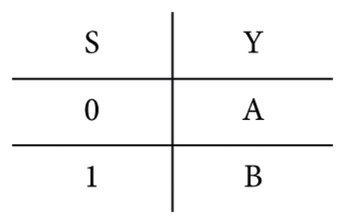
Block diagram, truth, and condensed tables of a 2 × 1 Mux are presented in Figures 8(a)–8(c), respectively. In the designed Mux, port 4 is always ON and input ports are considered as A and B states. Selector and output ports are assumed as S and Y states, respectively.
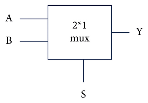
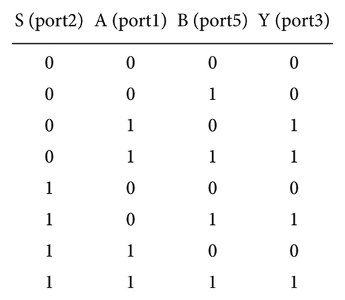
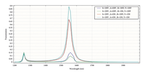
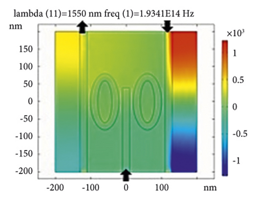
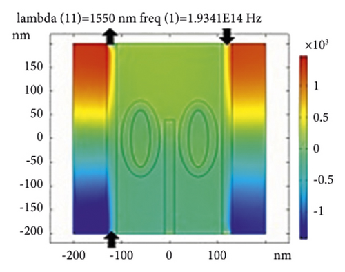
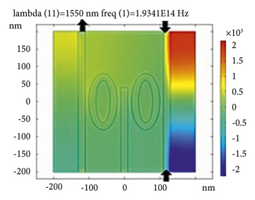
As shown in Figure 9(a), when the states of input ports, A and B states, are OFF or only B state is ON with 180° phase and the selector port, S, is OFF, the state of the output port of the multiplexer, Y, is OFF. According to the results, when the input ports are OFF, the transmission value is 0.12 at the operating wavelength. If only B is ON, the transmission value is 0.08 at a wavelength of 1,550 nm. The obtained transmission values at the operational wavelength are below the transmission threshold. As illustrated in Figure 9(a), when A and B are ON, or only A is ON, and S is OFF, constructive interference occurs between port A and port 4 or between port A and port B and the transmission increases. For ON output states, the transmission values are 0.68 and 0.89, above the transmission threshold.
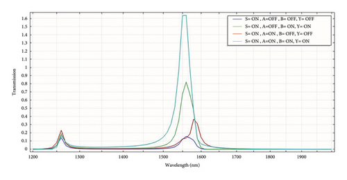
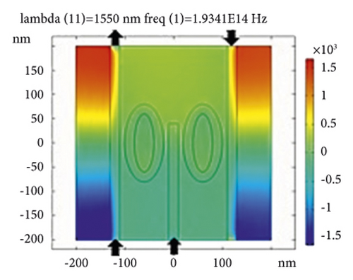
As shown in Figure 9(b), when the A and B states are OFF and S state is ON, with a phase of 180°, the destructive interference will occur between port 4 and selector port (S). In this case, transmission is 0.12, and the Y state is OFF. When the states of A and S are ON, and the phase of A signal equals 180°, the destructive interference will occur between port A and selector port (S), and the transmission value is 0.12, so the state of output port (Y) will be OFF. According to Figure 9(b) and the truth table in Figure 8(b), when the selector and input B ports are ON and port A is OFF, the constructive interference occurs between B port and selector port, and the output port is ON. In this case, the transmission value is 0.68. When inputs and selector ports are ON, the transmission exceeds 100% (1.63), resulting from constructive interference between the inputs and selector signals. The contrast ratio of this structure is 7.25 dB, and its performance is moderate, according to the authors in reference [41]. In addition, the recommended structure dimensions are excellent and optimal based on the MD value of 95.09%. Moreover, according to Tables 6 and 7, the IL and CL are moderate. The simulation results are summarized in Table 8.
| S (port 2) | A (port 1) | B (port 5) | T threshold | T | Y (port3) | CR (dB) | MD (%) | IL (dB) | CL (dB) |
|---|---|---|---|---|---|---|---|---|---|
| OFF | OFF | OFF | 0.5 | 0.12 | OFF | 7.25 | 95.09 | 1.67 | 5.57 |
| OFF | OFF | ON | 0.08 | OFF | |||||
| OFF | ON | OFF | 0.68 | ON | |||||
| OFF | ON | ON | 0.89 | ON | |||||
| ON | OFF | OFF | 0.12 | OFF | |||||
| ON | OFF | ON | 0.68 | ON | |||||
| ON | ON | OFF | 0.12 | OFF | |||||
| ON | ON | ON | 1.63 | ON |
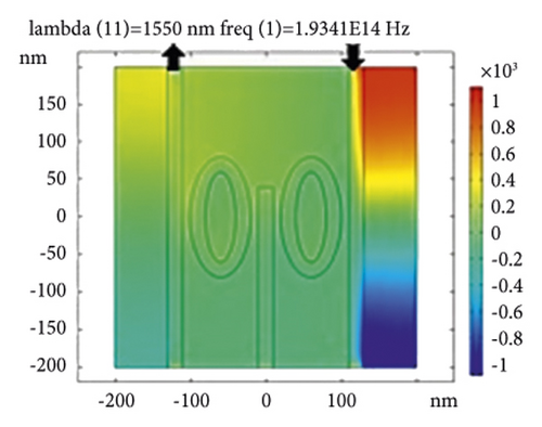
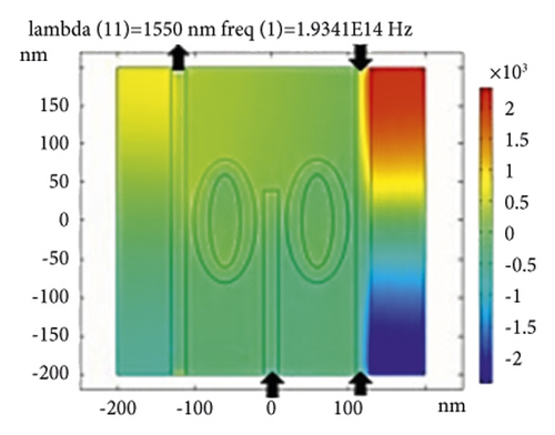
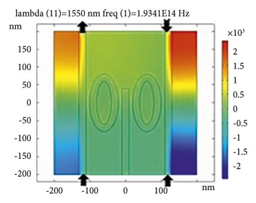
The z-component of the magnetic field, Hz, distribution, for all cases due to its truth table is shown in Figures 10(a)–10(h). The color bar in Figures 10(a)–10(h) illustrates the variation in light power intensity; the evolution from blue to red demonstrates that the light power intensity increases from low to high.

5. Comparison of the Proposed Work with Prior Works
The proposed structure is compared with the previous works as summarized in Table 9. As can be seen from Table 9, the proposed structure has good characteristics and the overall performance of our proposed work is more reasonable than the others.
| Reference | Topology | Size | Metal model | Number of resonators | Threshold limit | Operating wavelength | Performance measured by | Max. T | Structure complexity | Method used |
|---|---|---|---|---|---|---|---|---|---|---|
| [28] | Nanoracetrack resonator side coupled to air (MIM) waveguide | 3000 nm × 2400 nm | Drude model | One | 0.5 | 685 nm, 793.2 nm | Two parameters | 70% | More | FDTD |
| [29] | Dielectric-loaded plasmonic waveguides | 5.7 μm × 2.105 μm and more than 8 μm × 1 μm | Not available | Two | Less than 0.5 | 1550 nm | One parameter | 80% | More | FDTD |
| [32] | Plasmonic unidirectional coupler (MIM) waveguide | 7.5 μm × 6 μm | Drude model | Did not use resonator | 0.33 | 650 nm, 850 nm | Two parameters | 100% | More | FDTD |
| [33] | (MIM) plasmonic waveguide | 9.2 μm × 7.8 μm | Not available | Y shape wave guide | 0.5 | 1550 nm | Two parameters | Less than 10% | More | FDTD |
| [44] | MIM plasmonic slot cavities | 1.055 μm × 1.055 μm | Drude model | Four | 0.5 | 650 nm, 850 nm | Four parameters | About 100% | More | FEM |
| [45] | Surface plasmonic resonance in optical ring resonators MIM configuration | About 2.5 μm × 1 μm | Drude model | Three | About 0.45 | 1133 nm, 1219 nm and 1456 nm | Three parameters | About 100% | More | FDTD |
| [46] | Hybrid plasmonic waveguides | About 41 μm × 20 μm | Not available | Did not use resonator | Not available | 1550 nm | One parameter | 99.2% | More | FEM |
| This work | Nanoellipse IMI nanoplasmonic waveguides | 400 nm × 400 nm | Johnson and christy data | one | 0.5 | 1550 nm | Five parameters | 163% | Lesser | FEM |
6. Conclusion
An all-optical 2 × 1 (Mux) with a new configuration based on elliptical IMI-plasmonic waveguides has been presented in this paper. The proposed structure, which operates at a wavelength of 1,550 nm, has a compact size (400 nm × 400 nm), is simple, and has low loss. The function of the structure is based on constructive and destructive interferences between input signal(s) and the selector signal. The performance of the proposed plasmonic Mux is characterized by five parameters as follows: transmission (T), contrast ratio (CR), modulation depth (MD), insertion loss (IL), and contrast loss (CL) at 1,550 nm. The transmission threshold between logic 0 and logic 1 states was considered to be 0.5. According to the results, the maximum transmission efficiency of the device was 163%, and the recommended structure dimensions are excellent and optimal based on the MD value of 95.09%. The simulation results were obtained using the finite element method (FEM) with COMSOL Multiphysics 5.4 software.
Conflicts of Interest
The authors declare that there are no conflicts of interest regarding the publication of this article.
Acknowledgments
We would like to express our deep appreciation for the article authored by Abdulnabi, Saif H., and Mohammed N. Abbas which was published in the AIP Conference Proceedings [47] in the field of research on optical demultiplexers and their nanoscale applications.
Open Research
Data Availability
The data generated during the current study will be made available by the corresponding author upon reasonable request.


