3-D Printed Circularly Polarized Open-Ended Waveguide Antenna Array Based on an In-Built Antipodal Exponential Groove Polarizer
Abstract
This paper presents a novel 3-D-printed circularly polarized (CP) open-ended waveguide (OEW) antenna array. It aims to provide a lightweight scheme for OEW array design and concurrently address the high fabrication complexity problem of conventional OEW arrays. To realize these, the proposed design adopts dielectric 3-D printing technology to build the main body of the array and employs electroplating to form the waveguide walls. To attain CP radiation, an in-built antipodal exponential groove polarizer is proposed and applied to a square waveguide. With the perturbation of the grooves, degenerate modes TE10 and TE01 can be excited simultaneously, and their differential phase can be 90 degrees, resulting in CP radiation. Moreover, a novel matching cube based on effective medium theory (EMT) is proposed for the antenna to mitigate the reflections at the waveguide aperture and therefore realize good impedance matching. To validate the design idea, prototypes for a single element and a 2×2 array were fabricated and measured. Experimental results show that their weights are 15 and 76 grams, and their axial ratio bandwidths (ARBWs) are 16% (5.45-6.4 GHz) and 11.1% (5.52-6.17 GHz), respectively.
1. Introduction
Open-ended waveguide (OEW) antennas are very classic in the antenna area. They usually have advantages such as wide band, low loss, stable radiation performance, etc., and therefore they have been widely employed in various applications, such as measurement, radar, and detection systems [1, 2]. In principle, they are very similar to horn antennas, and thus these two types of antennas are often seen as equivalent. Nevertheless, since these antennas are all based on waveguide structures, they usually suffer from bulky size and heavy weight. For their fabrications, conventional designs often adopt the metal machining technique; it usually needs to split the waveguide structure first and then assemble and solder the machined components at a later stage [3]. There is no doubt that the conventional processing technique is time-consuming, high-cost, and complicated. In contemporary wireless communication systems, the size, weight, and fabrication difficulty of the antennas are critical considerations. Therefore, addressing these problems for OEW or horn antennas is necessary.
To generate circularly polarized (CP) waves for these antennas, numerous approaches have been proposed in the past, and they can be generally categorized into three types. One simple way is to use two feeding ports for a waveguide supporting degenerate modes [4]. The orthogonal components required by CP radiation come from the degenerate modes, and the 90-degree differential phase is provided by an external phase shifter. However, this approach may lead to extra feeding loss, and the overall feeding network is complicated. Other than this, adopting external circular polarizers to the apertures is another common approach [5, 6]. However, these polarizers are usually relatively large in sizes. and their installations are difficult. Compared to these approaches, a scheme of using an in-built polarizer is more popular for OEW or horn antennas because it not only has a smaller size but also can effectively attain CP radiation. In the reported studies, metallic screen [7], stepped-septum [8], twisted ridge [9], and monogroove [10] were proposed. However, since the in-built polarizers need to place structures inside the waveguides, they may further increase the fabrication difficulty.
To address the problems mentioned above, in this paper, we propose a novel CP OEW antenna array design. It employs advanced 3-D printing and electroplating as fabrication techniques. As an emerging technology, 3-D printing has exhibited great advantages over conventional means in terms of complex structure processing, labor, and time costs. It has been widely employed in areas such as architecture, medical treatment, and aerospace [11]. In recent years, it has been successfully applied in antenna designs as well, which demonstrates the feasibility and superiority of this technology in the antenna area.
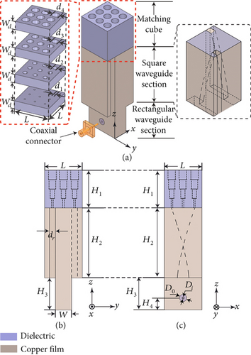
The proposed antenna adopts dielectric 3-D printing to build the main body of the antenna and uses electroplating to form the waveguide walls. It is essentially a dielectric-filled waveguide structure. Therefore, lightweight, compact size, and easy fabrication can be attained by it. To realize CP radiation, a novel in-built antipodal exponential groove polarizer is proposed and applied to a square waveguide. Moreover, to solve the impedance matching problem for the dielectric-filled OEW antenna, a matching cube based on effective medium theory (EMT) is proposed. In this paper, the design starts from the antenna element, and then a 2 × 2 array is proposed. Their prototypes were fabricated and measured. All the simulations were performed using the full-wave simulation software Ansys HFSS.
2. Design of the Element
2.1. Element Configuration
2.2. Impedance Matching
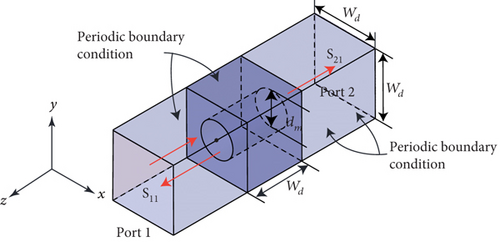
Since the antenna is essentially a dielectric-filled waveguide, an obvious air-dielectric interface exists at the aperture. This interface is a discontinuous plane for the waves when they propagate from the waveguide to the air. Therefore, strong reflections will be caused, resulting in severe impedance mismatching. For this reason, we designed the matching cube to mitigate the reflections. The core idea is to gradually change the effective permittivity of the dielectric to provide a smooth transition for the waves. According to the EMT, a small cubic unit cell with a length of Wd = 1/10λ0 (where λ0 is the free space wavelength at the center frequency) is proposed. In the simulation, this unit cell is placed inside a rectangular box whose side faces are assigned by a periodic boundary condition as shown in Figure 3. By extracting the S-parameters, the effective permittivity can be calculated. A detailed explanation of the EMT and the calculation method can be found in [12]. Figure 4 presents the calculated effective permittivity with different via diameters. It is seen that the effective permittivity can be altered with a change in the diameter. When the unit cell is fully filled (dm = 0 mm), the effective permittivity is equal to that of the material. While when the diameter is as large as the length of the unit cell (dm = 5.2 mm), the effective permittivity is close to that of the air.
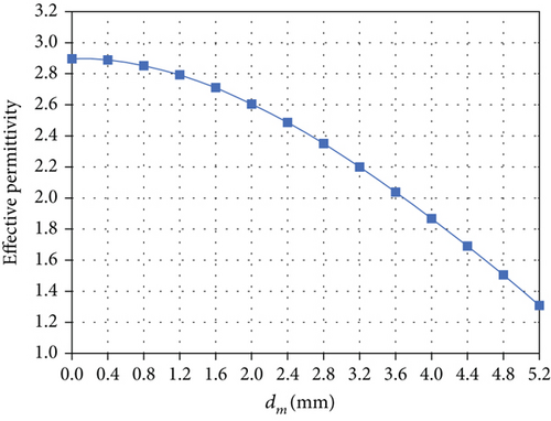
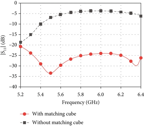
Based on these results, four diameter values are linearly selected for the matching cube, i.e., dm (m = 1, 2, 3, 4) equals 1.2 mm, 2.4 mm, 3.6 mm, and 4.8 mm, respectively, and the corresponding effective permittivities are 2.8, 2.5, 2, and 1.5, respectively. Figure 5 shows a comparison of |S11| with and without the matching cube. It is clear that the matching cube can significantly improve |S11| to a level of lower than −20 dB.
2.3. Operating Principle
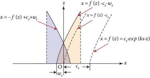
When the antenna operates, linearly polarized waves are first excited inside the waveguide. When they propagate to the square waveguide section, due to the antipodal configuration of the exponential grooves, the electric field will be perturbed in a tilted direction, as shown in Figure 6. According to the principle of vector decomposition, the incident electric field Ei can be resolved into two orthogonal components E1 and E2, which are corresponding to the degenerate modes TE10 and TE01 of the square waveguide. On the other hand, it is seen that the structures are different in the directions along x- and y-axes due to the grooves; therefore, the phase constants of the two components are also different. After a certain propagation distance (length of the grooves H2), the phase difference between the two components can be 90 degrees. Therefore, CP waves can be successfully generated. To validate this point, the electric field distributions above the element aperture for one time period T are investigated and presented in Figure 7. As the time changes, the electric field rotates in a counterclockwise direction. It indicates that the proposed antenna is able to realize CP radiation and the polarization state is right-handed CP (RHCP).
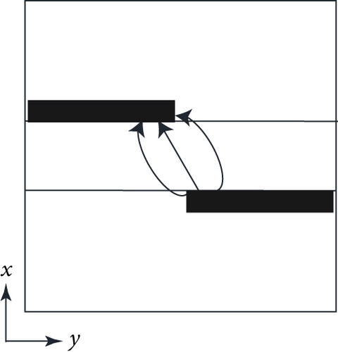
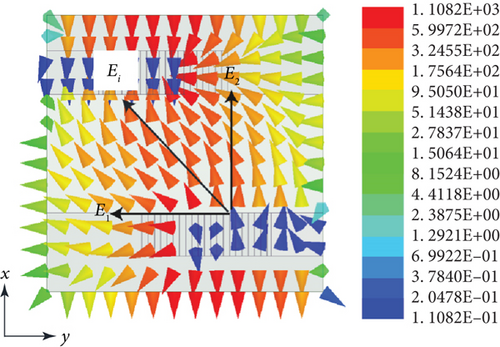
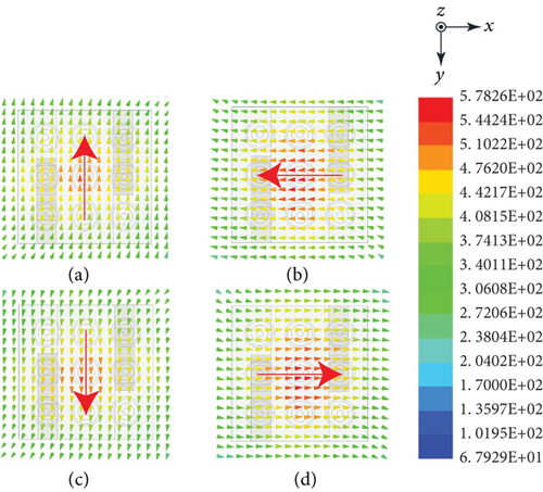
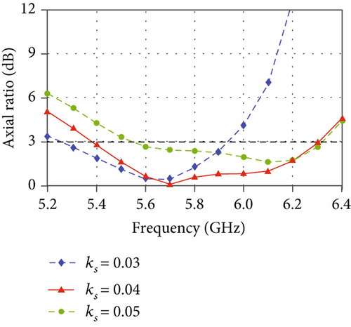
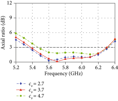
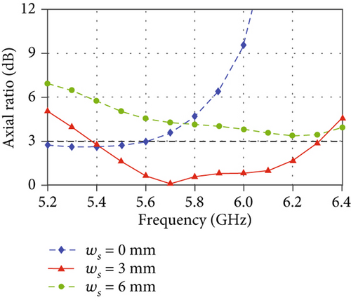
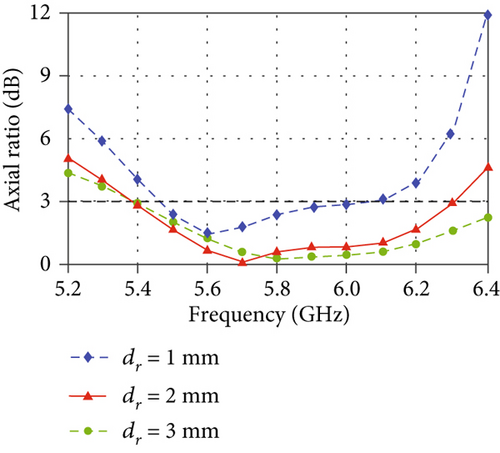
In Figure 8, the effects of some key geometric parameters on the axial ratio (AR) are presented. For the proposed antenna, the design of the grooves is critical. It is seen that the parameters ks and ws show relatively large impacts on the AR performance. They correspond to the length and overlapping size of the grooves, respectively. While the parameters cs and dr dominate the shape and thickness of the grooves, they have relatively small effects on the AR. When designing such an antenna, one can adjust the parameters ks and ws first to achieve an acceptable AR performance, and then use cs and dr to do the fine tuning.
3. Design of the 2 × 2 Array
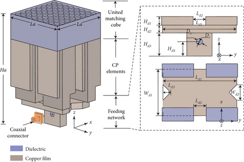
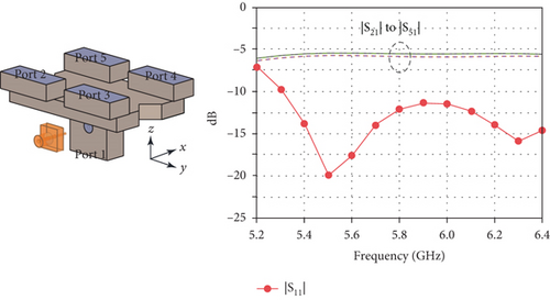
After the element design, a 2 × 2 antenna array is proposed. Its configuration is presented in Figure 9. The spacing of the elements is set at 30 mm corresponding, to 0.58λ0. Since we need to introduce mask structures to the matching cube section to prevent it from being plated during the electroplating process and since the separated design of the matching cubes of the four elements will increase the complexity and difficulty of the masking process, the four cubes are united as one piece in the array design. By using this way, the electroplating process can be simplified, while we found that the array performance remained the same compared to the separated case. Apart from this change, the geometric parameters of the elements are identical to the previous design. The feeding network adopts a four-way power divider. Its configuration and simulated S-parameters are presented in Figure 10. The input power can be equally allocated to the four elements. The insertion loss of each way is lower than 0.3 dB.
4. Antenna Fabrication and Performance
To validate the proposed design idea, an element and an array were fabricated and measured. Figure 11 shows the photographs of the fabricated prototypes. During the fabrication, the dielectric parts were first printed by a high-precision 3-D printer Stratasys J750. The printed material is a resin type with the same parameters as the ones we used in the simulation. Then, 3-D printed masks are applied to the prototypes to cover the surfaces that do not need cooper films. Finally, electroplating was processed for the waveguide walls, and the masks were removed. The coaxial connectors were installed using cyanoacrylate adhesive.
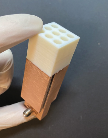
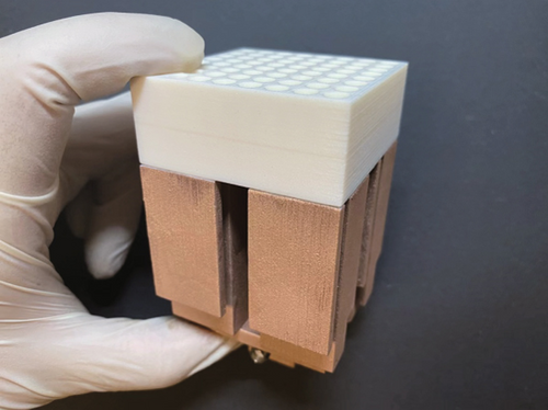
Figure 12(a) presents the measured and simulated |S11| of the proposed antenna element. It is seen that the element is matched from 5.2 to 6.4 GHz with |S11| lower than −15 dB.
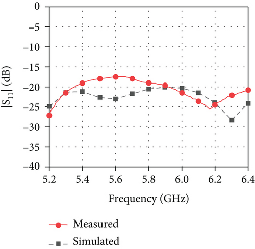
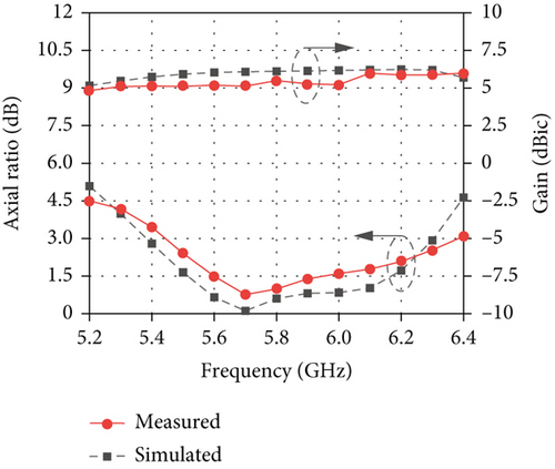
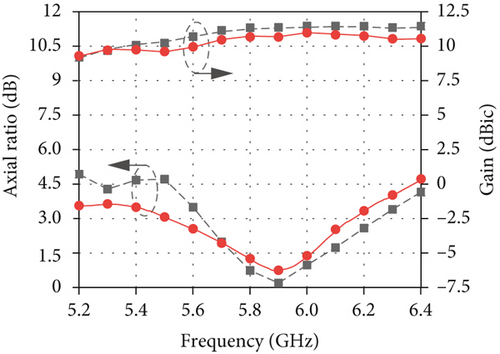
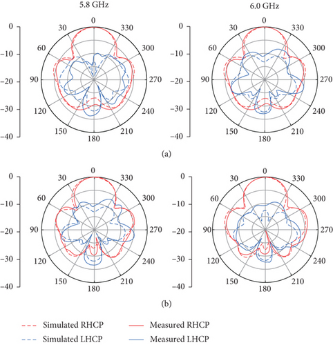
Figure 12(b) shows the measured and simulated ARs and gains. The measured results agree well with the simulated ones. The measured 3 dB ARBW is 16.4% from 5.45 GHz to 6.4 GHz. While within this bandwidth, the measured gain is 5.6 ± 0.6 dBic. The measured and simulated radiation patterns at 5.8 GHz and 6 GHz are exhibited in Figure 13. It can be observed that measured patterns show reasonable agreements with the simulated ones. Some small discrepancies are attributed to the measurement tolerance.
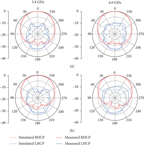
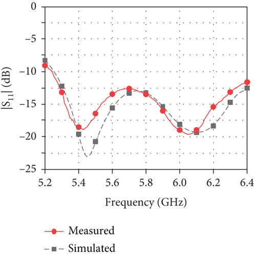
In Figure 14(a), the measured and simulated |S11| of the proposed antenna array are presented. The measured result agrees well with the simulated one and is lower than −10 dB from 5.25 to 6.4 GHz. The AR and gain results are presented in Figure 14(b). The measured 3 dB ARBW is 11.2% from 5.52 to 6.17 GHz. The measured peak gain is 11.1 dBic for the array, and the gain variation is lower than 1.8 dB within the 3 dB ARBW. Figure 15 shows the measured and simulated radiation patterns at 5.8 GHz and 6 GHz of the proposed array.
In Table 1, the proposed antenna element and array are compared to some reported CP horn antennas with in-built polarizers. It is seen that the proposed designs show superior performance on physical dimensions, fabrication difficulty, and antenna weight compared to the conventional designs. Due to their smaller size, the proposed antennas have to sacrifice some of their ARBW and gain performance; however, they are still capable of handling most applications.
| Ref. | Ant. type | Freq. (GHz) | Dimensions (λ0 × λ0 × λ0) | 3 dB ARBW | Gain (dBic) | Fab. method | Fab. difficulty | Weight |
|---|---|---|---|---|---|---|---|---|
| 7 | Element | 15.8 | NG | ≈4% | 14 | Machining + PCB | High | Heavy |
| 8 | Element | 85 | 3.2 × 3.2 × 16.2 | 21% (AR < 5.8 dB) | 20.3 | Machining | High | Heavy |
| 9 | Element | 10 | 0.95 × 0.95 × 5.9 | 51% | 10.1 | Metal 3-D printing | Easy | Heavy |
| 10 | Element | 57 | NG | 7.9% ∗ | ≈12 | Machining | High | Heavy |
| This work | Element | 5.8 | 0.43 × 0.43 × 1.56 | 16% | 6.2 | Dielectric 3-D printing + electroplating | Easy | 15 g |
| 2 × 2 array | 1 × 1 × 1.93 | 11.1% | 11.1 | 76 g |
- NG stands for not given. ∗This is an overlapped bandwidth of the impedance bandwidth and ARBW of this antenna.
5. Conclusion
In this paper, a 3-D printed CP OEW antenna element with an in-built antipodal exponential groove polarizer and its 2 × 2 array have been proposed, analyzed, fabricated, and tested.
The experimental results agree with the numerical predictions, which demonstrate that the proposed designs have the advantages of compact size, lightweight, and easy fabrication. They could be potentially applied in various CP applications.
Conflicts of Interest
The authors declare that they have no conflicts of interest.
Acknowledgments
This study was supported by the National Natural Science Foundation of China (grant/award number: 61901175), Guangzhou Science and Technology Foundation Basic and Applied Basic Research Project (grant/award number: 202102020861), and Natural Science Foundation of Guangdong Province (grant/award number: 2022A1515010254).
Open Research
Data Availability
Data sharing is not applicable to this article as no datasets were generated or analyzed during the current study.


