[Retracted] A 516 μW, 121.2 dB-SNDR, and 125.1 dB-DR Discrete-Time Sigma-Delta Modulator with a 20 kHz BW
Abstract
This article proposed a discrete-time single-loop 3rd order 5-bit Sigma-Delta (ΣΔ) modulator for the audio applications. In this modulator, a feed forward path is used to relax the design requirement of amplifier, which can reduce integrator’s output swing. And a 5-bit asynchronous SAR ADC combined with analog summing is adopted to quantify the summation of feedforward signal and loop filter output, which can significantly reduce power consumption. In addition, chopper stabilization technique is used to alleviate the flicker noise introduced by the first integrator. To eliminate the nonlinearity introduced by multibit quantizer, an improved data weighted average algorithm calibration circuit is proposed. The proposed modulator is implemented in 130 nm technology with a 1.12 mm2 core area. Operating at a 2.56MS/s sampling rate, post layout simulation results show that the modulator realizes 121.2-dB SNDR and 125.1-dB DR in a 20 kHz signal bandwidth, it dissipating 516 μW from 1.5 V supply. It also achieves the energy efficiency, as demonstrated by a Schreier figure of merit (FoMS) of 197 dB.
1. Introduction
High quality audio devices often require analog-to-digital converters (ADCs) with high resolution and energy efficiency [1]. Among different ADC topologies, ΣΔ ADCs can easily get high signal-to-noise-plus-distortion ratio (SNDR) above 90 dB by noise shaping and oversampling. So, they can avoid the need for complex calibration circuit or stringent matching between constituent elements [2]. Compared with other ADCs, ΣΔ ADCs are more energy-efficient and robust, and dominate the low-bandwidth high-precision signal processing applications. The ΣΔ ADC consists of an analog modulator and a digital filter, while analog modulator is the core circuit of the Sigma-Delta ADC. Among them, the continuous-time (CT) Sigma-Delta modulator (DSM) does not require high build-up speed of the integrator, which is beneficial for low-power design [3]. However, its signal path characteristics (e.g., noise shaping function) are closely related to the process-voltage-temperature (PVT) variation, the modulator has more stringent component matching requirements, and the SNDR is sensitive to clock jitter [4, 5]. The signal path characteristics of the discrete-time (DT) Sigma-Delta modulator is determined by the capacitance ratio, which has better tolerances for PVT variations and clock jitter. Compared to CT DSM, DT DSM can achieve higher resolution and linearity [6].
In DT DSM design, to improve energy efficiency, the DSM topology by reducing the analog filter input signal amplitude has been proposed. These alleviate the performance demands of SC integrator. One architecture adopts a multi-bit quantizer and input feedforward path [7]. Another is the 0-L multistage noise shaping structure, for which the first stage uses a multi-bit Nyquist ADC and the second stage uses L-order DSM [8]. On the circuit level, using switched capacitors or dynamic amplifier to implement integrators can effectively reduce power consumption [9, 10]. However, the gain of passive integrator is very low and the normal operation of dynamic amplifier often requires strict control conditions. So, the robustness and resistance to process parameter drift of the modulator is weak, and ultimately achieve only moderate resolution [11].
In this paper, we proposed a 5-bit DT DSM with feed forward path. An improved current mirror structure amplifier is adopted to drive the large sampling capacitor, and a 5-bit asynchronous successive approximation-register (SAR) ADC combined with analog summing is employed to replace the traditional flash-type quantizer. Integrating the advantages of high accuracy DSM and low power SAR ADC, the proposed modulator achieves high accuracy and energy efficiency. In addition, a low temperature drift bandgap reference is integrated on-chip to further improve system’s integration and reliability. The fabricated prototype achieves a dynamic range (DR) of 125.1 dB and a peak SNDR of 121.2 dB in 20-kHz bandwidth and dissipates 516 μW from 1.5 V supply with core area of 1.12 mm2.
This article is organized as follows: the architecture of proposed modulator is briefly described in Section II; the key circuit’s implementation details of the DSM are provided in Section III; simulation results are given in Section IV; section V draws the conclusion.
2. Modulator Architecture

Where NTF(z) denotes noise transfer function and STF(z) denotes signal transfer function. STF(z) maintains unit gain within the bandwidth, and NTF(z) can achieve third-order noise shaping. The magnitude-frequency response and root mean square (RMS) gain of the NTF(z) within bandwidth is shown in Figure 2. NTF(z) has an aggressive noise shaping ability. However, its gain factor in pass band is close to 20 dB which results in a smaller input range and poorer stability of the modulator. Therefore, this paper adopts a 5-bit quantizer to reduce quantization noise, and the finer quantization step reduces the voltage and current variations at each time-step [12]. So, the amplifier in modulator requires less energy to respond to signal changes, which can improve the modulator’s stability and energy efficiency. To achieve 18-bit resolution, the oversampling ratio (OSR) of modulator is selected as 64.

The digital output is feedback to the analog loop via a 5-bit DAC and the data-weighted averaging (DWA) module is added to feedback loop to eliminate nonidealities from mismatch between the devices of DAC.
3. Circuits Implementation
3.1. Switched Capacitor Scheme
Figure 3 presents the schematic of proposed DT DSM. It contains three integrators, a 5-bit asynchronous SAR incorporated with passive adder, dynamic element matching (DEM), and bandgap reference circuit, etc. The first-stage integrator uses gate voltage bootstrap switch to achieve high-precision signal sampling.

Besides, the 2nd and 3rd integrators employ CMOS switches to reduce the switch on-resistance [13]. At the same time, the 1st and 3rd integrators share a set of switch network, which can reduce circuit design complexity.
Actual switch exists on the on-resistance, and the thermal noise introduced by sampling switch network will severely limit the modulator’s signal-to-noise ratio (SNR). Especially in 1st integrator, the thermal noise will be directly superimposed on the input signal, which has the greatest impact on modulator. Therefore, the total sampling capacitance value of 1st integrator is chosen as 17.5 pF for low thermal noise. The 2nd and 3rd integrators contributes less noise, their sampling capacitance is 576 fF and 720 fF, respectively.
To suppress low-frequency flicker noise, the 1st integrator adopts the chopper stabilization technique. As shown in Figure 3, the frequency of chopper is selected as half the sampling frequency, which contributes to achieve a better effect [14]. The feedforward input signal and 3rd integrator’s output are added up in SAR quantizer and output a 5-bit digital code. Then, the digital output is decoded to thermometer and sent to DWA module for calibration. Finally, 5-bit DAC complete the loop feedback.
3.2. Bootstrapped Switch
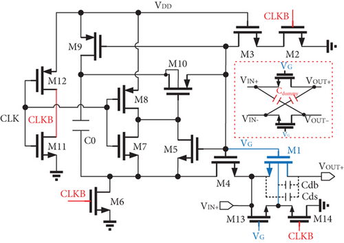
Figure 4 shows the bootstrapped switch, it is critical to ΣΔ modulator’s linearity. By adding a constant voltage across the gate-source of the M1, the on-resistance can be a constant while input varying. To eliminate the substrate effect, the sampling switch M1’s bulk is often connected to its source. However, when M1 turns off, the input can be coupled to Vout through the parasitic capacitance Cdb between the bulk and drain of M1, which brings errors to the sampling signal. Therefore, in this design, we selectively connect the bulk of M1 to its source and ground, which can solve this problem. The parasitic capacitance Cds exits between the source and drain of M1, it provides another coupling path. The effect of this path is mitigated by connecting a dummy capacitor between the drain of M1 and the other differential input.
3.3. Amplifier
Figure 5 shows the amplifier in 1st integrator. Since the nonlinearity and noise of later two integrators will be shaped by the 1st integrator, the requirements for gain and noise in 2nd and 3rd integrators can be relaxed appropriately. Thus, the design difficulty lies in the 1st integrator. The finite gain of amplifier will bring pole and gain errors into the integrator, resulting in quantization noise leaks. Therefore, high gain amplifier is necessary to alleviate this effect.
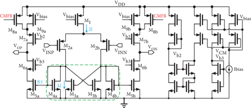
Where B is the current mirror ratio of M4a,b and M5a,b, k is the scale factor of M3a,b drawing current from M2a,b, gm2a,b is the transductance of M2a,b, and ro5a,b, ro6a,b, ro7a,b, ro8a,b, and ro9a,b denotes the equivalent impedances of the corresponding transistors. From the above equation, it can be concluded that current consumption technique boosts the gain of amplifier by 1/(1 k). In addition, the unit gain bandwidth product (GBW) of the amplifier is designed to 10FS to avoid a poor modulator performance due to inadequate setting of integrator.
Where γ is the excess noise factor of amplifier. From the above equation, it can be observed that thermal noise can be effectively reduced by increasing CS. For accuracy, power consumption, and area considerations, the value of CS in 1st integrator is set to the first stage integrator sampling capacitance value is set to 17.5 pF.
Simulation results show that the amplifier achieves a 72 dB of DC gain, the GBW is 25 MHz and phase margin is 67° at the load capacitance is 18 pF. The amplifier in 2nd and 3rd integrators use the same topology. Since the load capacitance of second stage is small, the transistors’ size is 1/5 of the first stage. The third stage needs to drive multi-bit quantizer, the transistors’ size of amplifier is 1/3 of the first stage. The Vbias, Vb2, and Vb3 is set by biasing circuit, and the current Ibias and common mode voltage VCM are generated by bandgap reference circuit.
3.4. Asynchronous Successive Approximation Quantizer
Due to the introduction of feed forward path, an analog summing circuit is required to add the input signal to the 3rd integrator’s output and send it to multi-bit quantizer completing the quantization. The asynchronous SAR quantizer proposed in this paper is shown in Figure 6(a). It consists of asynchronous logic, a dynamic comparator and a switch capacitors array. By designing appropriate operating timings and switching networks, the analog summing is embedded into the capacitor array to reduce the complexity and area of schematic. A common-mode voltage-stabilized capacitor switching strategy [16] is used by dividing the capacitance of bit 1-bit 4 into two equal parts and ensuring that the common-mode level at the comparator input is stable. Compared with conventional flash-type quantizers, asynchronous logic controlling the comparison process can avoid the use of high-frequency clocks, and single comparator operation can improve the modulator’s tolerance to offset. Combining with the low-power advantage of SAR ADC, the resolution and energy efficiency of the modulator can be improved effectively.
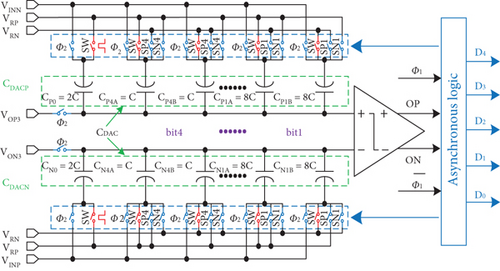
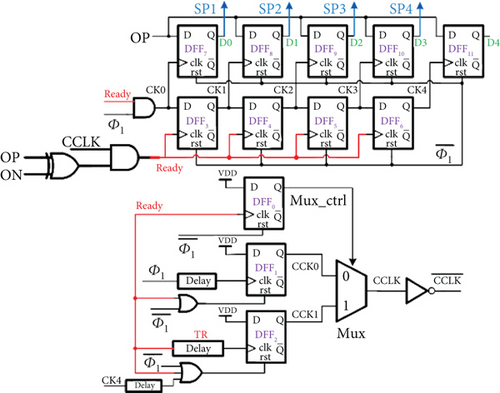
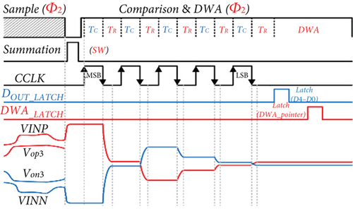
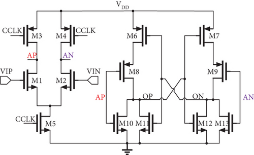
Figure 6(d) shows the comparator schematic in proposed asynchronous SAR quantizer. It contains a preamplifier and a latch, and adopts double-tailed fully dynamic latching structure to avoid the existence of static current. When CCLK is low, the comparator is stopped, Ap and An are charged to VDD, and Op and On are reset to GND; when CCLK is high, the charge stored in the parasitic capacitors of M1 to M4 is leaked by M5, which generates different current determined by the input voltage. This results in different rates of voltage drop at AP and AN nodes, thus generating a voltage difference ΔVAP,AN related to the input voltage. ΔVAP,AN is amplified by a positive feedback loop formed by M8 ~ M13 and create a comparison result. In addition, the interstage consisting of M10/M13 and M8/M9 provides an extra shield between the input and output to reduce kickback noise effectively.
3.5. Dem
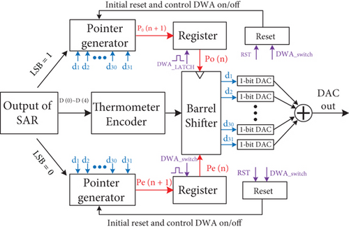
The main weakness of the multi-bit quantization modulator is that it is sensitive to the nonlinear error of DAC, which comes from the mismatch among the internal capacitor arrays. Therefore, a dual-pointer DWA calibration circuit is proposed in this paper to eliminate mismatch error and improve the linearity of the DAC. Depending on the parity of quantization results, different independent pointers are used to control the barrel shifter operation.
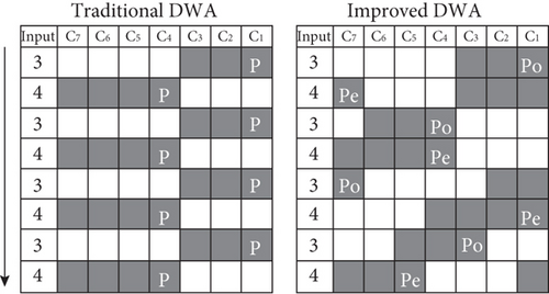
Figure 7 represents the principle of the conventional DWA and the improved DWA algorithm in a 3-bit DAC; white cells denote unused and dark cells denote the DAC cells being selected for use. P is the pointer of conventional DWA, Po is the pointer when the input value is odd and Pe is the pointer when the input value is even. It can be seen that although the input signal value appears regularly, the improved DWA algorithm does not cause the algorithm to fail due to regular selection of DAC units.
The DEM module is shown in Figure 8, including the thermometer decoder, pointer generator, barrel shifter, and reset circuit. The thermometer decoder converts the 5-bit binary code from SAR quantizer into 31-bit thermometer code; the pointer generator is the core logic circuit of the DWA algorithm, which generates the corresponding pointer according to the LSB value of digital output and determines the starting bit of the next barrel shifter operation. The reset module plays a protective role to avoid the pointer generator circuit being unable to recover itself due to interference. Besides, it performs initial reset of the pointer generator and controls DWA on and off. The barrel shifter is the execution circuit that cyclically shifts the input thermometer codes according to the starting bit determined by the pointer, and the shifted thermometer codes select the corresponding DAC units to complete feedback.
4. Simulation Results
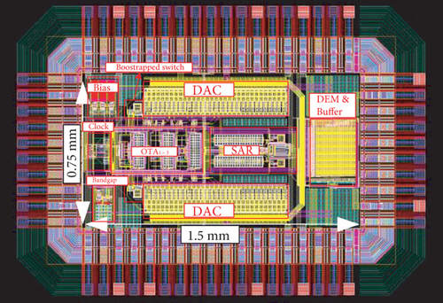
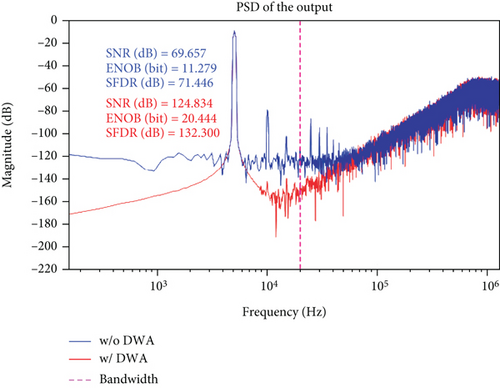
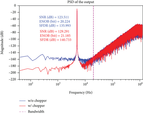
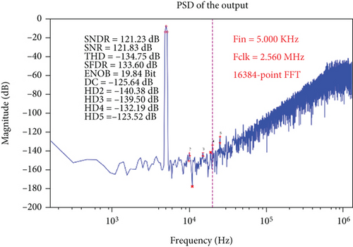
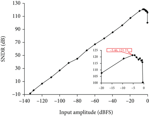
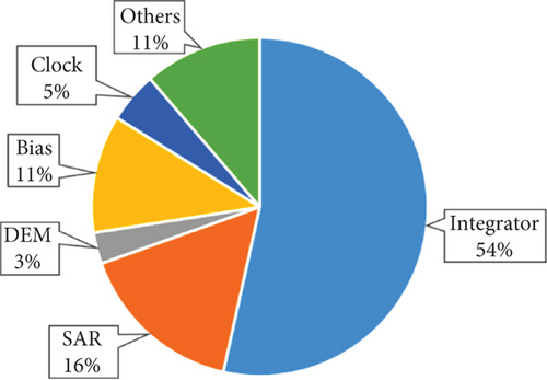
The proposed modulator is fabricated in 130 nm 1P7M CMOS process. Figure 9 shows the modulator’s layout. The core area is 1.5 × 0.75 mm2. Add 0.5% random mismatch to DAC capacitor array. Figure 10 shows the simulated output spectrum when the DWA is on and off. The mismatch among capacitors in the DAC causes serious harmonic distortion, which lowers modulator’s SNDR, but alleviating its impact via turning on DWA. As illustrated in Figure 11, chopper stabilization technology can suppress flicker noise in low-frequency, which improves the SNR within the bandwidth. The post layout simulated output spectrum is presented in Figure 12. The peak SNDR and SNR are 121.2 dB and 121.8 dB, respectively, as the input is a 5 kHz, −5.5dBFS sinusoidal signal. Figure 13 shows the post layout simulated SNDR versus input signal amplitude. The prototype modulator realizes a DR of 125.1 dB in 20 kHz bandwidth. Operating at a 2.56MS/s sampling rate, the modulator dissipates 516 μW under a 1.5 V supply. The breakdown of power consumption is presented in Figure 14.
The prototype modulator’ performance is summarized and compared in Table 1. Although the performance parameters of the modulator acquired from the post-layout simulation results, its Schreier figure of merits (FoMS) is up to 197 dB with efficient power consumption. As can be seen from Table 1, the prototype modulator achieves higher SNDR in the same bandwidth compared with other modulators. With different signal bandwidths, the prototype modulator has obvious advantages in energy efficiency, achieving an excellent balance between cost and performance.
| Technology [nm] | Supply [V] | BW [kHz] | FS [MHz] | SNDRPeak [dB] | DR [dB] | Power [mW] | FoMS(3) [dB] | AreaCore [mm2] | |
|---|---|---|---|---|---|---|---|---|---|
| [2] | 180 | 1.8 | 24 | 6.144 | 98.5 | 103.6 | 0.28 | 177.8 | 1.33 |
| [3] | 180 | 1.8 | 10 | 6 | 105 | 106.5 | 1.17 | 174.3 | 1.81 |
| [9](1) | 65 | 1.1 | 20 | 10 | 92.06 | 111.4 | 0.086 | 176 | — |
| [12] | 130 | 1.2 | 20 | 3.072 | 101.4 | 108.9 | 3.5 | 173.3 | 1.5 |
| [15](2) | 180 | 3.3 | 24 | 3.072 | 120 | — | 20 | 180.8 | 2.3 |
| This work(2) | 130 | 1.5 | 20 | 2.56 | 121.2 | 125.1 | 0.516 | 197.1 | 1.12 |
- (1) Schematic simulation results; (2) Post layout simulation results; Others are from measurements; (3)FoMS = SNDRPeak + 10log(BW/power).
5. Conclusion
In this article, a high-SNDR low-power audio DT DSM fabricated in a 130 nm CMOS process is presented. The modulator employs third single loop with 5-bit SAR topology. Feed forward path is introduced to reducing integrator’ swing. Adopting 5-bit asynchronous SAR ADC can avoid the use of high-frequency clocks, which can significantly reduce power and area consumption. Besides, an improved data weighted average algorithm calibration circuit is proposed to eliminate harmonic distortion. The post layout simulation results show that the proposed DT DSM achieves a peak SNDR of 121.2 dB with a 20 kHz bandwidth. It dissipates 516 μW under a 1.5 V supply.
Conflicts of Interest
The author declared that he has no conflicts of interest regarding this work.
Open Research
Data Availability
The experimental data used to support the findings of this study are available from the corresponding author upon request.


