[Retracted] A 146-dB-Ohm Gain 14-pARMS Noise Patch-Clamp Amplifier for Whole-Cell Ion Current Detection
Abstract
The membrane clamp technique is an important tool to reflect the electrophysiological characteristics of cells by recording the ionic currents of cellular channels. Embedded systems work in systems designed for specific user groups and are used to implement specific functions. The membrane clamp amplifier built with embedded technology has the advantages of miniaturization, specialization, low power consumption, high integration, high resource utilization, and a long life cycle, which can avoid the inconvenience to developers and experimenters due to the update of general-purpose computer software and hardware. In this paper, a patch-clamp amplifier (PCA) based on a transimpedance amplifier (TIA) is proposed, which includes a glass microelectrode series resistance/capacitance compensation circuit and feedback resistor parasitic capacitance compensation. The prototype is designed using 180 nm CMOS technology and occupies an area of 720 μm × 630 μm. The prototype achieves a transimpedance gain of 145.6 dB-Ohm, a -3 dB bandwidth greater than 15 kHz, and an input reference noise current of 13.98 pARMS. Experimental results show that the proposed PCA is capable of compensating up to 30 pF of electrode capacitance and up to 10 MΩ for 86% of the series resistance, respectively. In addition, when the feedback resistor parasitic capacitance compensation circuit is enabled, the overshoot phenomenon disappears, overcoming the shortcomings of the conventional diaphragm clamp amplifier current clamp and maintaining the original key performance.
1. Introduction
The diaphragm clamp amplifier design started in the late 1970s and gradually became a core instrument for electrophysiological measurements after the 1980s. It was originally designed to detect weak picoampere (10-12 A) currents in individual ion channels in conjunction with a high-resistance blocking technique [1], and thus, its core is a highly sensitive, ultralow noise I-V converter [2]. It was initially only suitable for voltage clamp experiments, and to be able to be used for current clamp experiments, a conventional diaphragm clamp amplifier A negative feedback method is used to make the cell membrane current track the current stimulus signal. Since it is not a direct current clamp and voltage measurement required for current clamp experiments, the negative feedback current clamp design shows inherent drawbacks, mainly in the form of current clamp errors and distortion and aberration of the membrane potential measurement signal. In 1996 and 1998, Magistretti made a detailed analysis of this problem [3, 4] and proposed to consider the diaphragm clamp amplifier as a “black box” to estimate the system type and response of the diaphragm clamp amplifier through the control and response of the external circuit model. The system type and parameters of the diaphragm clamp amplifier are estimated by the control and response of the external circuit model. Based on this estimation, various types of errors generated by the current clamp of the conventional diaphragm clamp amplifier are derived. He proposed an improvement scheme [5], but no improvement results have been reported since then. The work done in this paper, on the other hand, analyzes the root causes of distortion in the current clamp and membrane potential measurement response of the conventional diaphragm clamp from the internal structure of the conventional diaphragm clamp amplifier, making the necessary additions and corrections to Magistretti’s analysis.
Membrane clamp is an effective method for measuring cellular ionic currents [6]. This method is widely used in physiology to study the physiological functions of cells by recording the current changes of ion channels in the cell membrane [7]. The ion currents of single channels are typically on the order of pA; while in whole-cell recordings, the current is the sum of the currents of all ion channels on the cell membrane with an amplitude of several nA [8]. This requires a low-noise amplifier to sense such weak ion currents, which can also be used for nanopore sensing applications [9]. As shown in Figure 1, in whole-cell recording, by clamping the potential difference between the cell membrane and the signal ground, ionic currents from the cellular ion channels in the bath flow through a glass microelectrode and then into the detection circuit. To convert the current into a voltage for further processing, the current-to-voltage conversion can usually be achieved with the help of a transimpedance amplifier (TIA) [10].
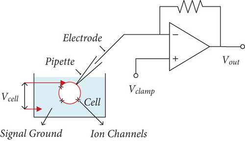
In whole-cell recording, the amplitude of the current is a few nanoamps over a bandwidth of 10 kHz, and the TIA enables continuous-time recording with a TIA resistance value in the range of a few MΩs [11, 12]. In conventional CMOS processes, high resistances occupy a large area of the layout and generate significantly large parasitic capacitances, which affect the stability of the circuit [13]. Typical values of electrode resistance are in the range of 5-20 MΩ. During the measurement, the current flowing through the electrode causes a voltage drop across this resistance, which causes the intracellular voltage Vm to deviate from the ideal clamp voltage Vclamp [14, 15]. Also, the electrodes have a large parasitic capacitance, which will have a significant impact on the stability of the circuit.
This paper is organized as follows: Section 2 first briefly describes the overall structure of the proposed patch-clamp amplifier (PCA), then the circuit details of the developed feedback resistor parasitic capacitance compensation and glass microelectrode series resistor/capacitance compensation are presented, and this section also analyzes the noise model and operational amplifier of the PCA; section 3 shows the experimental results of the whole PCA, followed by a summary in Section 4. The conclusions are summarized in Section 4.
2. PCA
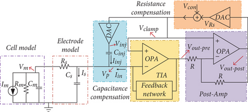
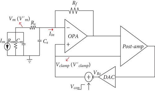
We propose a PCA with three compensation functions for whole-cell ion current detection. As shown in Figure 2, our PCA consists of four subblocks: (1) TIA; (2) postamplifier for converting ion currents to voltage; (3) capacitive compensation for feedback resistors; and (4) resistive/capacitive compensation circuit for electrodes. Table 1 shows the typical parameters of the whole-cell recording experiment and the design parameters of the PCA.
| Membrane resistance Rm (typical) | >GΩ |
| Membrane capacitance Cm (typical) | 10-100 pF |
| Series resistance of electrode Rs (typical) | 5-20 MΩ |
| Parasitic capacitance of electrode Cs (typical) | 5-15 pF |
| Membrane current Im | A few nA |
| Feedback resistance Rt | 20 MΩ |
| Feedback capacitance Cf | 500 fF |
The TIA as the first stage performs voltage clamping to the commanded voltage (Vclamp) concerning the experimental ground. When a control voltage (Vcon) is applied externally, the ionic current generated by the cell is converted to an output voltage by both the TIA and the postamplifier. The compensation circuits are used to compensate the parasitic resistor and capacitor of the microelectrode, and the DAC (digital-to-analog converter) in the compensation circuit is adopted to adjust the compensation ratio. The digital input of the DAC is provided by an external FPGA (field programmable gate array).
2.1. Parasitic Capacitance Compensation of the Feedback Resistor
As shown in Figures 3 and 4, the total feedback resistance (Rt) and parasitic capacitance (Ct) are divided into n segments, because this aggregation resistance will occupy a very large chip area for a CMOS process and will introduce large parasitic capacitance due to the presence of parasitic capacitance between the bottom aggregation layer and the substrate. The total parasitic capacitance (Ct) is estimated to reach ~8.24 pF. To convert the weak ion current to an output voltage in the mV scale, the resistor in the TIA is chosen to be 20 MΩ. In conventional schemes, a lumped capacitor is assumed to model the parasitic effect and is connected in parallel with the input of the TIA; however, when accurate frequency and transient simulation is required, using this simplified lumped model is not sufficient; therefore, we consider a distributed parasitic model.

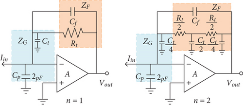
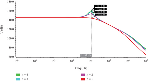
When setting n = 2, the damping factor ζ in (5) drops below unity; thus, the transfer curve has the potential to present overshoot which is not depicted by Equation (1). Figure 5 shows the closed-loop gain of the transfer function of the TIA with different values of n. Once n is 1, the amplitude is nearly flat within the interested frequency range. Upon setting n = 2, the gain overshoot begins to appear. The value of Cf must be increased to stabilize the TIA. The influence of distributed parasitic model on the stability of the system will be aggravated. The larger the n value is, the worse the stability of the system will be. Therefore, a compensation method should be adopted to ensure circuit stability under the premise of maintaining bandwidth. For 20 MΩ polyresistors, when n ≥ 4, the simulation results of the distributed parasitic model are relatively close. Therefore, n = 4 is fixed in this work to represent the parasitic model with large resistance.
As shown in Figure 6, the large feedback resistor is divided into 4 segments, and in the layout stage, different N-well regions are drawn under these segments. A simple source follower (SF) circuit is used for the compensation of each segment, where the input and output of the SF are connected between the subresistor node and its N-well node [16, 17]. Since in the conventional circuit, the polysilicon resistor is placed directly on top of the p-substrate, and since the p-substrate must be connected at the lowest potential, the polysilicon resistor is placed on top of the N-well, which is the bottom plate of the parasitic capacitor, to facilitate the voltage adjustment in this design. The poles generated by the feedback resistor and its parasitic capacitor will be shifted to a higher frequency, thus making the circuit more stable. Therefore, the voltage of the N-well can follow the voltage of the subresistor, the charging and discharging effect of the parasitic capacitor disappears, and the parasitic capacitance in the circuit can go to zero.
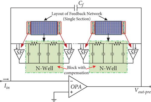
The source follower can be enabled or disabled to study the effect of the compensation circuit on the measurement, because the driving strength of the SF is designed to be sufficient to drive the induced parasitic capacitance between the N-well and the substrate, and the bandwidth of the SF is 48 MHz, which is sufficient to cover the bandwidth of the patch-clamp amplifier system.
2.2. Parasitic Capacitance Compensation
Considering the existence of the electrode parasitic capacitance (Cs can be estimated using a simple voltage clamp measurement), when the control voltage (Vcon) is applied externally, the voltage will charge/discharge Cs, resulting in a large transient current that will travel through the feedback network to disturb the output voltage. Meanwhile, the parasitic capacitance and the feedback resistor will form a low-frequency pole that affects the stability of the TIA. For these two reasons, compensation for Cs is very necessary. As shown in Figure 7, capacitance compensation is achieved by connecting the capacitor (Cinj) in parallel with Cs, and applying a voltage proportional to the Vcon at the other port of Cinj, the currents of Cinj and Cs are equal in magnitude and opposite in polarity.

When (6) is satisfied, the transient current of parasitic capacitance of the electrode is fully compensated.
2.3. Series Resistance Compensation
The series resistor (Rs can be estimated using a simple voltage clamp measurement) of the electrode has typical values in the range of 5-20 MΩ, when the current flows through the electrode, the voltage drop will be generated on the series resistor, and there is a voltage difference between the membrane potential Vm and external Vcon. Because this voltage difference complicates the object of studying the voltage/current characteristics of the cell itself, to alleviate this problem, the series resistance of the microelectrodes is usually measured before the experiment, and its effects are eliminated by numerical data algorithms. However, we still need to consider another drawback posed by this series resistance. With the membrane capacitance (Cm) typically in the range of 10-100 pF, the RC network composed of Cm and Rs results in a time constant of several mS, which slows down the establishment of the cell membrane potential and limits the bandwidth improvement of the PCA. Therefore, the series resistance compensation technique is proposed in the paper (see Figure 8).
2.4. Noise Analysis
Figure 9 shows the noise model of the TIA, as well as the input equivalent circuit. Although the noise of the PCA is mainly contributed by the TIA front-end and the battery electrode network, the noise of the postamplifier can be neglected due to the high gain of the front TIA [18, 19].
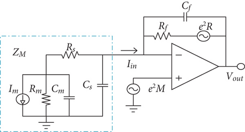
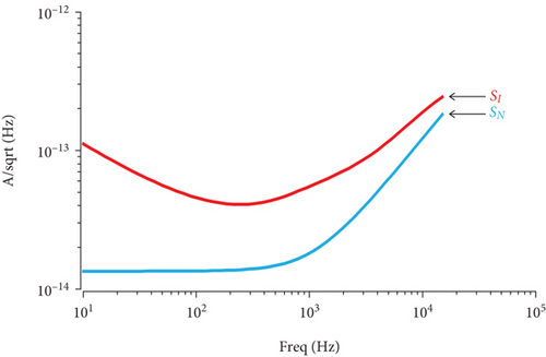
Figure 10 shows the simulated current noise power spectrum of SN compared with the total input current noise power spectrum. The flicker noise of the amplifier is the dominant noise source at low frequencies. At higher frequencies, SN is the dominant component of SI.
2.5. Operational Amplifier
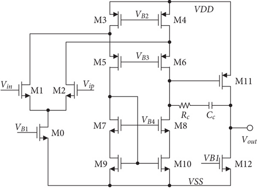
At low frequencies, the noise consists mainly of the thermal noise of the transistor and 1/f noise, where the thermal noise is proportional to the temperature and the 1/f noise is opposite to the frequency [20, 21]. The cross-conductance of the input differential pair is increased while the cross-conductance of the current mirror transistor is reduced to reduce the thermal noise of the op-amp. To reduce the 1/f noise of the op-amp, the size of the transistor can be increased, especially the size of the input differential pair. In addition, the PMOS input pair is placed in a separate N-well to isolate the noise from the substrate. Table 2 summarizes the performance of this op-amp. Figure 11 shows a low-noise three-stage op-amp in a PCA.
| Supply voltage | 3.3 V |
| DC gain | 127 dB |
| Gain-bandwidth product | 9.5 MHz |
| Phase margin | 60 dB |
| Equivalent input noise voltage (1-15 kHz) | 8.1 μVRMS |
3. Experimental Results
Figure 12 shows the chip photomicrograph of PCA, which has been fabricated in a 180 nm standard CMOS process and occupies the core area of 720 μm × 630 μm. Figure 13 shows the test fixture of the proposed PCA, and Cs, Rs, and Cm represent the electrode parasitic capacitance, electrode series resistance, and membrane capacitance, respectively. Cell membrane resistance (Rm) is too large which can reach 10 GΩ; thus, it is ignored in the test. The output voltage (Vout−post) of the PCA and clamping voltage (Vclamp) is connected to the oscilloscope. Tektronix AFG31252 signal generator provides the voltage signal and converts it into current through the R.
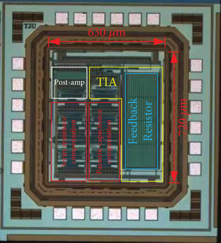

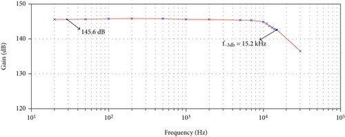
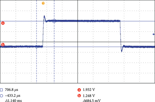
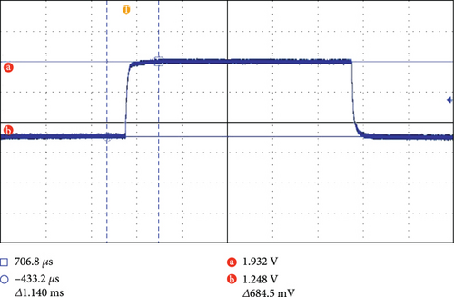
Figure 14 depicts the measured frequency response of our PCA. It scores a 145.6 dB-Ohm gain. and the -3 dB bandwidth is 15.2 kHz. Figure 15 shows the measured pulse responses of the PCA without and with the parasitic capacitance compensation for the feedback resistor. As predicted, the parasitic capacitance compensation circuit greatly alleviates the problem of transient rings.
Due to the limited input resistance of the oscilloscope, it is inaccurate to measure the voltage Vm. Therefore, the Vclamp is captured instead. With the test configuration, a current of 10 nA is injected, leading to a 100 mV voltage drop on Rs. To demonstrate the series resistance compensation, the control voltage (Vcon) is changed to 50 mV (typical 0-100 mV). The intended change of Vclamp is the sum of Vcon and voltage drop of Rs; thus, the change of the membrane potential Vm is the same as that of Vcon. Figure 16 shows the impact of the series resistance compensation with different compensation ratios. The blue curve represents the voltage change at the Vclamp. Figure 16(a) represents the Vclamp without compensation. Figures 16(b)–16(d) show the compensation effect when the compensation ratio is 20%, 50%, and 86%, respectively.
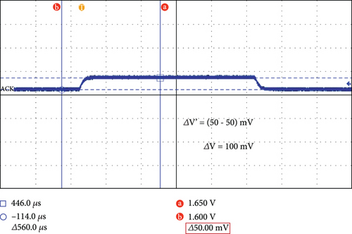
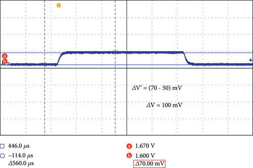
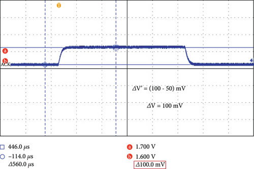
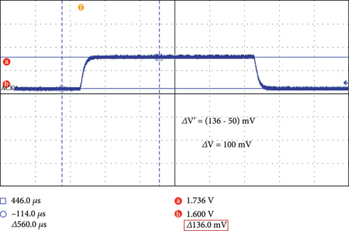
Figure 17 outlines the measured responses of our PCA while using parasitic capacitance compensation. Figures 17(a)–17(d) exhibit the uncompensated, partially compensated, optimally compensated, and overcompensated, respectively. The measurement results demonstrate that our design can compensate up to 30 pF electrode parasitic capacitance.
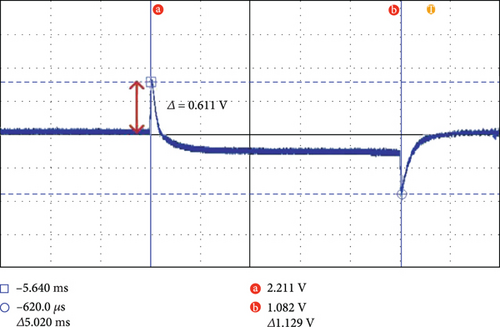
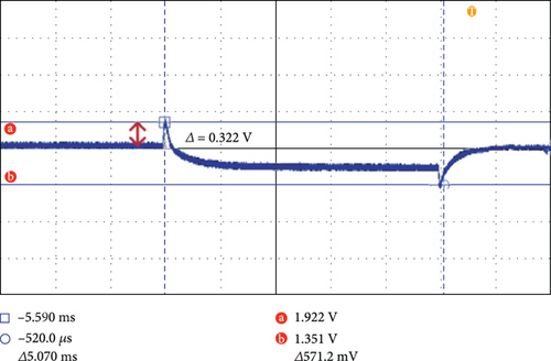
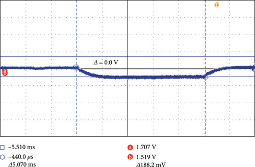
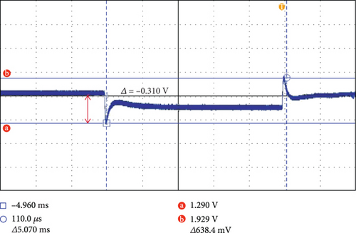
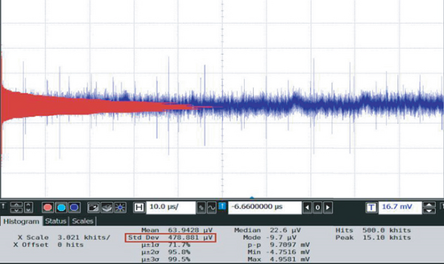
Table 3 summarizes the main performance of the proposed PCA compared to the prior art [22, 23] and commercial devices (Axopatch 200B) [20, 24]. The proposed design shows a wider bandwidth and higher capacitance compensation and is the only design that integrates a glass microelectrode series resistance/capacitance compensation circuit and feedback resistor parasitic capacitance compensation.
| Parameter | [13] | [16] | [17] | [18] | [19] | This work |
|---|---|---|---|---|---|---|
| Input-referred RMS noise (bandwidth) | 2.09 pA (10-10 kHz) | 5 pA (10 kHz) | 1.1 pA (5 kHz) | 3.3 pA (5 kHz) | 1.65 pA (5 kHz) | 13.98 pA (15 kHz) |
| Series resistance compensation | — | 0-4 MΩ | 0-32 MΩ | 0-100 MΩ | 0-100 MΩ | 0-10 MΩ |
| Electrode capacitance compensation | — | 0-20 pF | 0-10 pF | 0-10 pF | 0-10 pF | 0-30 pF |
| Rf parasitic capacitance compensation | Effective | — | — | — | — | Effective |
4. Conclusion
This paper reports a PCA with series resistance compensation, microelectrode parasitic capacitance compensation, and feedback resistor parasitic capacitance compensation for whole-cell ion current detection. The PCA has a gain of 145.6 dB-Ohm, a -3 dB bandwidth over 15 kHz, and an RMS noise of 13.98 pA. It can compensate the capacitance and resistance of the electrodes up to 30 pF and 86% of the series resistance, respectively. Feedback resistance parasitic capacitance compensation can effectively improve the stability of the TIA and can eliminate output voltage overshoot.
- (1)
Further improvement of the application functionality. This application only has a simple display and zoom function in this aspect, and more functions can be considered to add to facilitate the experimenter to analyze the results
- (2)
Data acquisition card sampling rate enhancement. The current data acquisition card can work at a sampling rate below 100 k. When the sampling rate is higher than 100 k, it will cause Linux scheduling problems and make data errors. The solution is to add RAM to the data acquisition card so that the data is first stored in RAM and then read into the application after the acquisition is completed by a Linux scheduling. The hardware part of this solution has been completed, and a new driver needs to be designed to solve the sampling rate problem
- (3)
Noise reduction. At present, the noise of the test data acquisition card reaches about 20 mV, and after using the regulated voltage to power the digital part of the system separately, the noise is also between 10 and 20 mV, so it is necessary to further reduce the noise
- (4)
Increase the storage method. Diaphragm clamp experiments often take a long time and will produce sa large amount of data, and the system Flash memory only has 64 M of space. The solution is to use a USB flash drive to store data, and the current system has been able to identify the USB flash drive, but the system does not automatically mount; you need to write a program to achieve automatic mounting of the USB flash drive. Hard disk can also be used to store data, which not only requires hardware support but also requires the design of hard disk drivers
- (5)
Network control. The system has a network interface and can access the network to transfer files. Further research can be done to achieve remote operation of the embedded system using the network. By establishing a server in the embedded system, the remote computer sends control commands, the server gives these commands to the application program to process, and the embedded system running the application program can also transmit the experimental information and experimental data to the computer client
- (6)
Improve the embedded diaphragm clamp amplifier system. At present, this system has preliminary results in both hardware module and software module, and the next step can be considered to combine these resources to conduct biological experiments. It is believed that with the continuous development of embedded technology and the increasingly widespread application of diaphragm clamp technology, the embedded diaphragm clamp amplifier system will have a broader prospect of use
Conflicts of Interest
The author declared no conflicts of interest regarding this work.
Open Research
Data Availability
The experimental data used to support the findings of this study are available from the corresponding author upon request.


