[Retracted] Improvement and Reduction of Self-Heating Effect in AlGaN/GaN HEMT Devices
Abstract
GaN is one of the third-generation broadband semiconductor materials developed rapidly in recent years, and Algan/GanHEMT has a broad application prospect in the fields of high temperature, high power, high frequency and radiation resistance, etc. In recent years, gallium nitride based high electron mobility transistors have been widely used in emerging industries, such as 5G technology, new energy vehicles, unmanned aircraft and other fields, due to their high power and high voltage resistance. However, due to the high power density of HEMT devices, the self-heating effect will lead to a significant increase in the junction temperature of the device, which will seriously affect the performance, reliability, and lifetime of the device. In this paper, the temperature characteristics of GaN high electron mobility transistors (GaN HEMTs) are studied, and the effect of self-heating effect on GaN HEMT devices is analyzed. In order to reduce the device temperature and improve the reliability of the device, a new device structure is proposed in this paper. The new structure replaces the conventional silicon and Si3N4 with highly thermally conductive diamond and SiC as the substrate and passivation layer of the device, which facilitates the heat dissipation from the substrate and passivation layer. Also, the new structure employs a hybrid barrier layer and field plate. Simulation results show that the new structure has about 30% lower temperature peak, 47% higher output current, 28% higher transconductivity, and up to 18.22% higher current collapse rate compared to the conventional structure.
1. Introduction
Over the past decades, human society has entered the information age, and the semiconductor industry has stepped into the fast lane of development, gradually becoming an indispensable part of people’s lives. With the continuous progress of science and technology, people have put forward higher requirements on the performance of semiconductor devices. Power devices based on gallium nitride (GaN) materials such as HEMT and MESFET have been widely used in 5G technology, new energy vehicles, unmanned aircraft, and other emerging industries with broad application prospects [1, 2]. GaN is a third-generation semiconductor material, which has the characteristics of wide forbidden band, high critical breakdown electric field, and high electron saturation rate compared with the first and second generation semiconductor materials. It can be seen that GaN materials have a forbidden band width of 3.39 eV and a critical breakdown electric field of 3.3 mV/cm, which are well suited for making high-power, high-frequency devices [3, 4].
AlGaN/GaN heterojunctions were first born in the 1990s and were successfully prepared on sapphire substrates by metal organic chemical vapor deposition (MOCVD) in a study by [5]. A year later, the first GaN-based HEMT device was developed by [6]. In recent years, GaN-based HEMT devices have become a research hotspot in the semiconductor industry due to the rise of 5G technology. The advantages of GaN HEMTs come from two main properties: a wide 3.39 eV forbidden band and a high concentration of two-dimensional electron gas (2DEG) accumulated at the heterojunction interface [7, 8]. 2DEG exhibits a very high electron mobility at room temperature (>2000 cm2/V -S) at room temperature, which gives HEMT devices superior power density and frequency.
When high currents flow through HEMT devices, the self-heating effect causes a significant increase in the junction temperature of the device and impairs the output characteristics of the device. It is known that the failure rate of electronic devices increases with temperature and is more significant at higher temperatures, which means that reducing the device junction temperature can significantly improve the device lifetime [9]. The traditional package level heat dissipation technology cannot effectively solve this problem, and the heat dissipation capability of GaN HEMTs must be improved from within the device. Nowadays, SiC materials with high thermal conductivity are usually used as the substrate for GaN HEMTs, but for higher power density HEMT devices, SiC substrates are difficult to meet the demand of fast heat dissipation; therefore, finding alternative substrate materials with better heat dissipation capability becomes one of the important ways to solve the self-heating problem of HEMT devices.
The thermal conductivity of diamond material is the highest among all known natural materials, up to 1000-2000 W/m-K, depending on the crystal structure, growth method, growth quality, and ambient temperature of diamond. Combining GaN epitaxial layers with diamond can significantly enhance the heat dissipation capability of HEMT devices. Natural diamond (SCD) is extremely expensive and difficult to fabricate large-size films, and GaN (GOD) HEMT devices on diamond substrates have been widely reported in recent years with the further development of synthetic polycrystalline diamond (PCD). PCD has the same structure as SCD, similar thermal conductivity, and substantially lower cost and is currently the most commonly used material for diamond substrates [10]. It has been shown that diamond substrates can increase RF power by a factor of 3.6, reach a power density of 56 W/mm (at DC), and significantly reduce the device junction temperature compared to HEMT devices on SiC substrates [11]. However, the conventional substrate materials have low thermal conductivity, and the devices do not dissipate heat significantly. In addition, it is a challenge to meet the demand for high-frequency and high-power devices, which severely limits GaN HEMT devices to unlock their original potential. Therefore, using a material with high thermal conductivity as a substrate or device heat sink layer can effectively improve the self-heating effect. Solutions that only change the material have limited thermal effect and must also change the device structure. Study [12] mitigated the self-heating effect of sapphire substrate devices by using a flip chip structure. Study [13] proposed the use of AlN and Si3N4 materials as double passivation layers for the devices and investigated the effect of their thickness on the electrical properties. The study [13] showed that the peak temperature of AlN decreased by 160 K at a thickness of 5 nm, and the most significant improvement in current and transconductivity was obtained.
To reduce the self-heating effect, the material and structure of the device are changed in this paper, and diamond and SiC with higher thermal conductivity are used as the substrate and passivation layer of the device, as well as the hybrid barrier layer and field plate to make the device suitable for operation at high power and high temperature.
2. Device Structures and Models
In this paper, AlGaN/GaN device is simulated using the Silvaco TCAD software, and the referenced device structure is shown in Figure 1. The substrate material is Si with a thickness of 2.45 μm, the buffer layer GaN with a thickness of 2.25 μm, and the potential barrier layer Al0.26Ga0.74N with a thickness of 23 nm. The thickness of the GaN bubble layer below the gate is 4 nm, where the doping type is n-type and the concentration is 1e20 cm-3. The thickness of the passivation layer Si3N4 is 2.47 μm. The length of both source and drain is 0.5 μm, and the gate length is 0.25 μm. The gate-source spacing is 0.77 μm, and the gate-drain spacing is 1.32 μm. In 2019, the study [14] increased the power density of InGaN HEMT to 22.3 W/mm by adding PCD film at the bottom of the HEMT device and reducing the thickness of the SiC substrate and improving the backside polishing process and significantly reduced the boundary thermal resistance of SiC/PCD, which is schematically shown in Figure 1. In addition, the gate is a Schottky contact, while the source and drain are ohmic contacts. To reduce the lattice mismatch between the buffer layer GaN and the substrate silicon, an AlN nucleation layer with a thickness of 0.05 μm is grown between them [9].
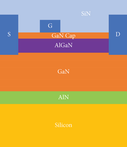
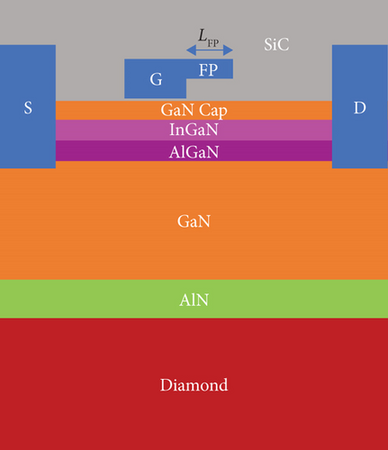
This paper is mainly divided into two steps to reduce the device temperature. Firstly, the substrate material Si of the conventional GaN HEMT device is replaced with diamond, and Si3N4 is replaced with SiC as the passivation layer. The structure of the device is shown in Figure 2(a). Using materials with high thermal conductivity in the substrate and passivation layer enhances the device’s ability to dissipate heat vertically, facilitating heat dissipation from the substrate and passivation layer. Secondly, a mixed barrier layer is used, and the structure of the device is shown in Figure 2(b). The barrier layer under the gate is divided into two layers: the upper layer is an In0.15Ga0.85N thin layer with an optimal thickness of 0.5 nm, and the lower layer is AlGaN. In addition, the device uses a field plate with an optimal field plate length of 0.3 μm and a field plate thickness of 35 nm.

In this paper, a variety of models are used for simulation. Due to the presence of two-dimensional electron gas, GaN HEMT devices have high electron mobility, so the simulation adopts the mobility model.
GaN HEMT devices will generate a lot of heat at the channel during operation, and this heat will diffuse to other locations through heat conduction. Therefore, a lattice heat transfer model and a heat generation model are used. The thermal conductivity of each layer material is different in GaN HEMT devices. In order to improve the accuracy of the simulation, the thermal conductivity model of the material is introduced. Considering that the generation and recombination of carriers are related to temperature, the simulation also adds the SRH model. At the same time, the polarization model is also used in the simulation.
3. Simulation Results and Discussion
3.1. The Effects of Self-Heating Effect on Device Performance
In order to compare the effect of self-heating effect on the output curve of GaN HEMT devices, simulations were performed for conventional device structures. During the simulations, the gate-source voltage was varied from -2 to 0 V, and the drain voltage was varied from 0 V to 15 V. Figure 3(a) shows the output curve without considering the self-heating effect, which shows that the drain current does not drop rapidly when the drain voltage exceeds the knee point voltage. Figure 3(b) shows the output curve considering the self-heating effect, and it can be seen that the output current shows a significant drop at larger drain voltages, while at smaller gate voltages, the self-heating effect has less effect on the output current of the device.
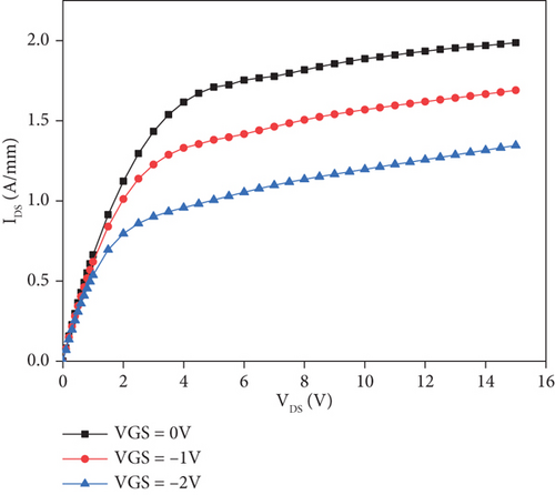
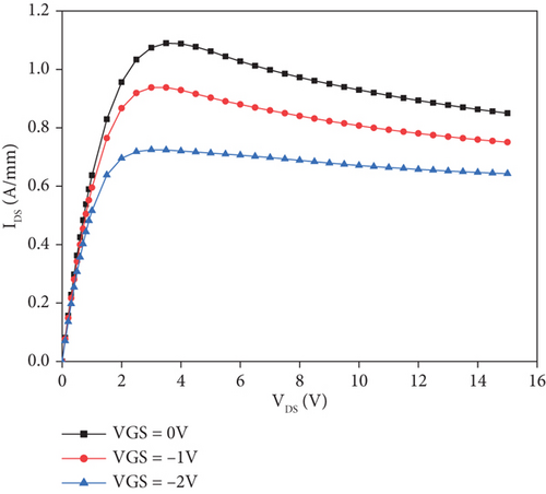
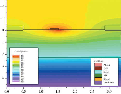
Figure 4 shows the temperature distribution of the device at VGS = 0 V. It can be seen that the temperature peak is 493 K when the substrate material of the device is Si and Si3N4 is the passivation layer. As shown in Figure 4, the temperature peak appears around the gate, and the maximum drain current is 1.08 A/mm. The simulation results show that the self-heating effect leads to the degradation of the device and reduces the performance of the device.
3.2. Effects of Diamond and SiC Materials on Device Temperature
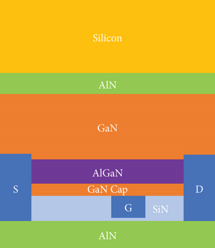
The material’s thermal conductivity coefficient limits the device’s heat dissipation capability, and the higher the thermal conductivity, the better the heat dissipation. In this paper, diamond material with high thermal conductivity is used as the substrate, and SiC material is used as the passivation layer. A flip-chip structure is also incorporated to highlight the contrast, as shown in Figure 5. The flip-chip structure is the original device structure upside down; the entire device buckled in the substrate. The dimensions of the flip-chip structure are the same as those of the referenced device structure.
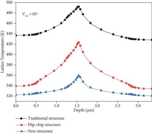
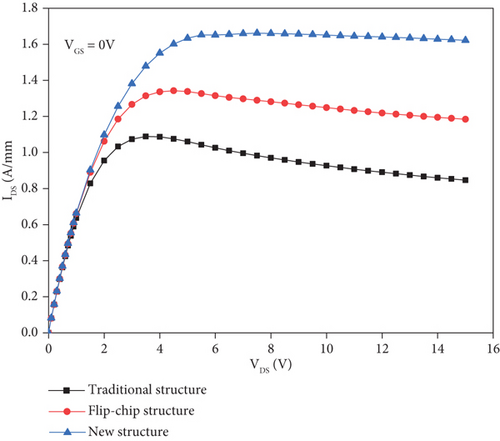
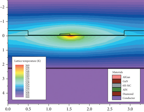
Figures 6 and 7 show the channel temperature distribution curves and output curves for different device structures, respectively. It can be seen that the flip-chip structure with AlN substrate has a channel temperature peak of 424 K and a maximum output current of 1.35 A/μm, while the device structure with diamond as the substrate and SiC as the passivation layer has a channel temperature peak as low as 360 K and a maximum output current of 1.65 A/μm. Compared to the conventional device structure, the temperature peak of the device structure with diamond substrate and SiC passivation layer decreases by 133 K. In addition, the drain current increased by 0.57 A/μm, and the current collapse was also significantly improved. Figure 8 shows the temperature distribution of the device structure with diamond substrate and SiC passivation layer. Due to the high thermal conductivity of diamond and SiC materials, the temperature is lowest in the substrate and passivation layer and highest near the channel. Therefore, the temperature difference allows the heat to be dissipated from both the substrate and the passivation layer. In addition, the temperature distribution near the channel is more uniform.
3.3. Effects of the Mixed Layer and Field Plate on Device Temperature
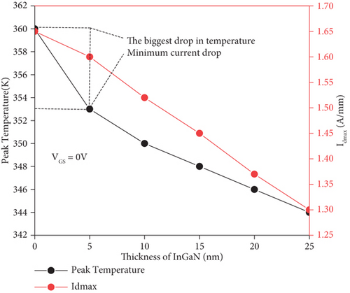
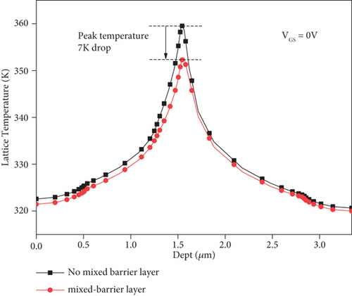
There is a limit to reducing the temperature of the device by changing the material. To further reduce the temperature of the device, the structure of the device must also be changed. Firstly, a new structure of the mixed potential layer is presented in this paper. The barrier layer under the gate is divided into two layers: the upper layer is an In0.15Ga0.85N, and the lower layer is AlGaN. Figure 9 shows the effects of InGaN thickness in the potential barrier layer on the peak temperature and maximum output current. As can be seen from the figure, the temperature peak and maximum drain current decrease as the thickness of InGaN increases. When the thickness of InGaN is 5 nm, the channel temperature peak is 353 K, and the maximum drain current is 1.60 A/mm. This is when the peak channel temperature drops the most, and the current drops the least. When the thickness of InGaN is greater than 5 nm, the temperature peak drops slowly while the maximum drain current drops sharply. The heterojunction formed by InGaN and AlGaN induces a polarized negative charge, which decreases the electron concentration of the two-dimensional electron gas and leads to a decrease in the drain current. As a result, the temperature of the device can be reduced. In summary, the optimum thickness of InGaN is 5 nm. Figure 10 shows a comparison of channel temperatures for InGaN thicknesses of 5 nm, with a 7 K drop in peak channel temperature and a more uniform channel temperature distribution for the structure with the hybrid barrier layer than for the structure without the hybrid barrier layer.
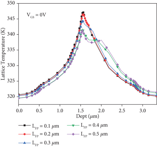
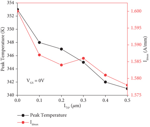
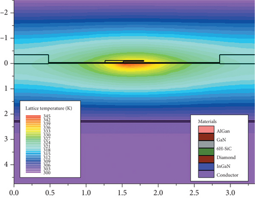
Secondly, the field plate is added at the gate near the drain, and the length of the field plate also impacts the device’s performance. Figure 11(a) shows the effects of the length of the field plate on the channel temperature. As the length of the field plate increases, the channel temperature’s peak gradually decreases, and the temperature spreads outward in a small way. Another peak in the channel temperature of the GaN HEMT device occurs when the length of the field plate is greater than 0.3 μm. At the same time, it has been detrimental to reduce the channel temperature of the device. Figure 11(b) shows the effects of field plate length on maximum output current and peak temperature. There is no new peak in channel temperature, and the output current is the nearby maximum when the channel length is 0.3 μm. Although the use of field plates reduces the temperature, it also reduces the electron mobility and decreases the maximum output current of the GaN HEMT. As can be seen from the figure, the maximum output current decreases, then increases, and then decreases as the field plate length increases. Therefore, combined with Figure 11, it can be concluded that the optimal length of the field plate is 0.3 μm when temperature and output current are considered together. In addition, the thickness of the dielectric layer of the field plate is 35 nm. As shown in Figure 12, the final temperature of the device is 345 K through material and structural changes, achieving a significant temperature reduction.
3.4. Analysis of Other Electrical Characteristics
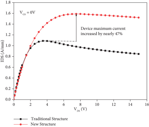
GaN HEMT is a high-power device, and the magnitude of the saturation drain current has been an essential characteristic of the output characteristics. Figure 13 shows the comparison of the drain current between the conventional device structure and the new structure. The saturation drain current of the conventional device structure is 1.08 A/μm, while the maximum saturation drain current of the new structure is 1.586 A/μm, an improvement of about 47%. The current density increases due to its relationship to electron mobility and electric field. When the temperature of the device decreases, the lattice scattering effect decreases, and the electron mobility increases, which in turn increases the current density. The current collapse is also critical to the reliability of the device. Applying a linear approximation to the saturation region portion of the output characteristic curve, the current collapse rate of the conventional device is 22.5%. The new structure uses diamond and SiC materials, as well as a mixed barrier layer and field plate, to reduce device temperature, improve the electron mobility of the channel, and reduce the effect of temperature on device output characteristics. The current collapse rate is only 4.28%, and the improvement ratio is 18.22%, achieving significant improvement in the current collapse effect.
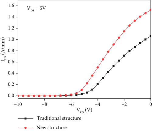
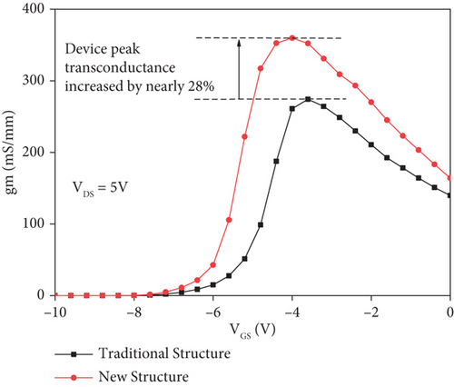
The transfer curves of the conventional and new structures are shown in Figure 14(a). As can be obtained from the figure, the threshold voltage of the conventional structure is -5.01 V, while the threshold voltage of the new structure is -5.56 V, which means that the device can be turned off at a lower voltage. Transconductance indicates the ability of the gate voltage to control the drain current. The larger the transconductance, the stronger the gate voltage control to the channel. Figure 14(b) represents the transconductance curves of the conventional device structure and the new structure, which significantly improves transconductance compared to the conventional device structure. The peak transconductance of the conventional device structure is 282 mS/mA, while the peak transconductance of the new structure is 360 mS/mA. Compared with the peak transconductance of the traditional device structure, the peak transconductance of the new structure is increased by about 28%, indicating that the device’s gate voltage has dramatically improved the control ability of the channel.
4. Conclusion
GaN HEMT devices have a wide range of applications in high-frequency and high-power fields. The research on GaN HEMT devices has made great progress so far, but with the high-power nonapplication, the increase of channel temperature caused by the self-heating effect of the device makes the thermal reliability problem become more and more serious. In this paper, the temperature of GaN HEMT devices at high bias voltage is reduced by changing the material and structure. The maximum temperature of the reference device structure is 493 K. The new structure uses diamond and SiC with high thermal conductivity as substrate and passivation layer to enhance the device heat dissipation in the vertical direction. Simulation results show that the new structure reduces the temperature by about 30%, increases the output current by 47%, and improves the transconductivity by 28% compared to the conventional structure. In addition, the current collapse improvement can reach 18.22%. Therefore, this new structure is suitable for operation at high temperature and high power, improving the reliability of GaN HEMT devices. The main goal for the future is to develop a multiphysics field 3D electric-thermal-force coupling model, which is expected to extract the device junction temperature and thermal stress more accurately. In this paper, specific experimental steps are lacking, and the relevant simulation data are obtained based on ideal cases, which need to be further verified in real situations. In the future, the process of GaN epitaxial layer preparation on diamond substrate can be improved to optimize the thermal characteristics of the device.
Conflicts of Interest
The authors declared that they have no conflicts of interest regarding this work.
Open Research
Data Availability
The experimental data used to support the findings of this study are available from the corresponding author upon request.


