Improved GA and Its Application in Performance Optimization of Electronic Components
Abstract
In order to improve the performance optimization effect of electronic components, this paper uses the improved GA to construct the performance optimization system of electronic components. Moreover, this paper proposes an optimized reliability allocation process method based on cost function, which further optimizes the reliability design of electronic circuit systems. In addition, this paper conducts a sensitivity analysis of the electronic circuit system and compares and analyzes the evaluation results of component sensitivity and comprehensive importance based on simulation. Finally, this paper compares and demonstrates the different influences of various components in the electronic circuit system on the whole system. The experimental research shows that the performance optimization system of electronic components based on the improved GA proposed in this paper has a certain effect on improving the performance of electronic components.
1. Introduction
With the development of science and technology, the classification and characteristics of basic electronic components are becoming more and more detailed. Moreover, the detection of electronic components also presents the characteristics of many types of tests, complex parameters, and high complexity. At the same time, the detection data of electronic components shows the characteristics of large amount of data and heterogeneous structure. In the face of a large amount of data formed in production inspection, traditional electronic component inspection methods have been unable to adapt to this development trend. Therefore, electronic component manufacturers and product quality inspection institutions need to have more reasonable and applicable methods to deal with this development trend.
Data collection based on the Internet of Things, data mining of big data, and cloud computing remote measurement technology are all reasonable and effective methods and means that can be applied to the detection of electronic components. This paper aims to change the current testing methods in the production and testing of electronic components, so as to effectively improve the information level of traditional industries, significantly improve the production efficiency of enterprises, and create good social and economic benefits for enterprises [1]. Starting from the informatization testing method for the detection of physical parameters of electronic components, research on the key basic common problems in the detection of electronic components, and find an informatization method to analyze and process a large amount of heterogeneous data generated in the detection of components, and address the methods and means of measurement, transmission, storage and analysis of relevant data. Relying on the gradually mature informatization application technologies such as Internet of Things technology, big data mining, and cloud computing, the traditional electronic component detection method is moved towards the direction of informatization processing [2].
With the advancement and development of science and technology, higher and higher requirements are put forward for the quality of products. The quality of the product is measured by the degree of consistency between the performance index of the product and the specified standard value. In practical engineering problems, there are inevitably a lot of uncertain factors, and these factors will cause the technical parameters of the product to deviate from the specified standard values, resulting in quality loss. Many companies try to reduce these uncertainties in the manufacturing and trial stages to improve product quality, but doing so often increases costs with little success [3]. With the in-depth study of uncertainty, high-tech enterprises have clearly realized that the control and assurance of product quality must seek the source; that is, the quality of products is first designed, and then applicated [4]. Current product design methods tend to ignore a wide range of uncertainties, such as lack of knowledge of personnel, design flaws, manufacturing errors, and variability in operating environments, which can have significant impact on product performance. The quality control method has a large impact and even causes critical failure when it lose control [5]. The influence of uncertain factors greatly increases the risk of system failure. Electronic systems (products) are composed of various components. The system structure and functions are increasingly complex and diversified, and they play a very important role in the fields of civil industry, national defense, and military [6]. Electronic components in electronic systems are affected by uncertain factors such as material properties, processing technology, and working environment during manufacturing, assembly, and use. There are often deviations between actual parameter values and nominal values. The cumulative effect of the deviation will improve the performance of the system. The response deviates from the target value and even causes failure [7]. If these uncertain factors are treated as deterministic information, this may lead to problems such as low consistency of batch products and extremely sensitive products to external interference factors, which cannot meet the actual requirements of engineering [8]. In the early design and analysis stage of electronic systems, noise factors and fluctuations in design parameters are ignored, which makes it difficult for the system to achieve stable performance and at the same time ensure reliability requirements. The complex electronic system model of the formula does not fully consider the computational complexity of the system model and the discrete characteristics of design variables, resulting in low efficiency of system optimization and difficulty in obtaining discrete optimal solutions [9]. How to consider the influence of various uncertain factors as comprehensively as possible in the optimization of electronic systems and take corresponding measures to improve the robustness of products is an urgent problem to be solved [10].
With the development of computer optimization technology, designers try to find the optimal solution from the perspective of mathematical optimization equations, which makes the optimization process of robust optimization design more scientific. Scholars take the first derivative of the objective function with respect to the design variables of interest as the optimization objective, in order to make the objective function value insensitive to changes in the design variables. This method is also known as the robust optimization design method based on first-order sensitivity, and its relatively direct and high computational efficiency has been applied by many scholars. Literature [11] takes the first derivative of the performance function as the optimization objective to optimize the structure of the electromagnetic device so that the device performance remains robust to changes in electric and magnetic fields. However, methods based on first-order sensitivity are often considered inaccurate. Literature [12] regards the second-order derivative of the performance function as the optimization objective and combines the worst-case analysis and Taguchi method to simplify the calculation in the optimization process. The goal of robust optimization design based on sensitivity is usually to improve the ability of the system to resist external noise interference, without considering the performance offset introduced by the system’s own structural dimensions and material properties, and the optimization results are usually not practical. Another approach that starts with a mathematical optimization equation perspective is robust optimization design based on random distributions. It represents all uncertain parameters contained in the objective function and constraints as random quantities in a certain distribution form, takes the mean and variance of the output performance of the system as the optimization objective, and searches for a solution that satisfies the constraints and has the smallest objective value [13]. The main disadvantage of this method is that after introducing random variables, a large number of target and constraint values need to be evaluated in the optimization process; in particular, for complex engineering problems with finite element solution or electronic circuit simulation, the optimization speed becomes very slow. In order to improve the optimization speed, the optimization design technology based on approximate model began to develop. Approximate models such as Kriging model, radial basis function, and multilayer neural network model are used to approximate the system output value, which greatly shortens the optimization time [14]. Reliability-based optimal design is also an effective method for optimal design of uncertain systems, and the obtained optimal solution can satisfy the product with low failure rate under this parameter combination [15]. According to the coupling strategy of reliability analysis method and optimization design method, reliability-based optimization design methods can be divided into two categories: double-loop method and single-loop method [16]. The single-cycle method is an improvement to the double-cycle method, so that the reliability analysis process is separated from the sub-cycle of the optimization process and is in the same cycle, thereby improving the optimization efficiency. Literature [17] proposed a single-cycle univariate method. By transforming the parameter distribution and its related objective functions and constraint functions into a standard normal distribution space, the original optimization problem was redefined by using the partial derivative of the constraint equation to make it a single-cycle optimization problem. Literature [18] used the sequential optimization and reliability evaluation method to change the order of the optimization process, verified the constraints in the probability-based optimization loop, and equivalently regarded the probability-based optimization problem as a deterministic optimization problem.
In this paper, BP neural network (GA-BP) learning graph algorithm model based on genetic algorithm is used to predict the non working reliability parameters of electronic components. After testing, the GA-BP prediction model has better accuracy than the linear autoregressive prediction model. At the same time, it also broadens the application scope of neural network, which can be used as a new method for nonoperating reliability life prediction of electronic components.
The main organizational structure of this paper is as follows: Section 1 presents an introduction, which analyzes the research status and background, summarizes the literature views, and leads to the research content of this paper. Section 2 describes the improvement of the nonworking performance analysis algorithm of subcomponents in this paper. The performance optimization and intellectualization of electronic components are very important. Section 3 provides the construction of the algorithm model and the performance verification. Section 4 summarizes the content proposed in this paper and looks forward to the follow-up research.
In this paper, using the improved GA, the performance optimization system of electronic components is constructed to improve the working performance of modern electronic components.
2. Optimal Design of Electronic Circuit System Based on Importance Analysis
2.1. Reliability Model
According to the analysis in this section, the numerical calculation of the comprehensive importance of the power conversion main circuit is shown in Table 1.
| Component node | Comprehensive importance |
|---|---|
| C1 | 0.23634 |
| Q1 | 0.327543 |
| Q2 | 0.174326 |
| D1 | 0.68781 |
| D2 | 0.215433 |
| RL1 | 0.000202 |
| RL2 | 0.187052 |
| L | 0.522776 |
It can be seen that the order of the cmprehensive importance of the components is D1 > L > Q1 > C1 > D2 > RL2 > Q2 > RL1 without considering the control circuit. The importance of diodes, inductors, and switches is the highest, and the importance of sampling resistors is relatively low.
Based on the evaluation results of comprehensive importance and complexity, the comprehensive importance is normalized, and the sum of the importance is obtained according to the principle of the AGREE distribution method, as shown in Table 2. It is the basis of reliability allocation, as shown in (2).
| Component node | Normalization |
|---|---|
| C1 | 0.34360 |
| Q1 | 0.69930 |
| Q2 | 0.25350 |
| D1 | 1.00000 |
| D2 | 0.31320 |
| RL1 | 0.00030 |
| RL2 | 0.27200 |
| L | 0.76010 |
It can be seen that the distribution results meet the reliability index requirements of the power conversion main circuit.
In the formula, i is the component serial number, Fcost is the target cost, λS is the system failure rate, and λG is the expected system target failure rate. λimin, λimax are the minimum and maximum values of the failure rate of component i, which can be obtained according to the previous reliability distribution based on importance and historical data of similar products.
λQ is the work failure rate of switch tubes Q1, Q2Q1, Q2; FcostQ is the cost of switch tubes Q1, Q2Q1, Q2; λD is the working failure rate of the freewheeling diodes D1, D2D1, D2; FcostD is the cost of the diodes D1 and D2; λC is the working failure rate of the input filter capacitor C1C1; and FcostC is the cost of the capacitor C1.
According to the optimized allocation of component failure rate and the working environment of the power conversion main circuit system, we can further select the model through the selection of parameters of various influencing factors by referring to the manual and historical data. Here, only the freewheeling diode D1 is taken as an example for description.
In the formula, λ is the working failure rate, λb is the basic failure rate, E is the environmental coefficient, Q is the quality coefficient, R is the rated value coefficient, A is the application coefficient, K is the type coefficient, and C is the structural coefficient. These parameters can be selected with reference to the electronic product reliability prediction manual.
It can be seen that the basic failure rate λb obtained based on the work failure rate of comprehensive importance analysis is 0.1144∗10−6/h, and the basic failure rate calculated based on the optimized work failure rate of cost-optimized allocation is 0.1146∗10−6/h.
2.2. Sensitivity Analysis
Sensitivity analysis is a local analysis, including finite difference method, direct derivation method, and Green’s function method. It should be noted that this method is not suitable for scenarios of nonlinear models and when there are uncertain input factors of different orders of magnitude.
The electronic circuit system belongs to the time-dependent dynamic system, so the direct derivation method can be used, and the differential or differential-algebraic formulas can be used to describe it.
The global sensitivity, also known as the importance measure, focuses on the situation when all the input factors change together and each factor comprehensively evaluates the sensitivity in the whole working time and state range. It is a method to analyze the severity and importance of the influence of all uncertain factors and component parameter changes on the output of the system. It comprehensively considers the probability distribution of each input factor, has a wide expansion range, has a large variation range of controllable parameters, and selects the key design variables of the system through accurate evaluation. When using global sensitivity analysis, the model is not limited. At present, the Sobol variance decomposition method is the most widely used global sensitivity analysis method, and a brief introduction is given below.
2.3. Model Construction of Electronic Circuit System in Simulation Software
The dual-tube buck-boost topology is applied to the power conversion circuit, and the traditional control method of the power conversion circuit adopts the two-mode control method. That is, at any time, only one switch is guaranteed to be controlled. When Uin > Uo, the switch tube Q1 is in the normal working state of the switch, and the switch tube Q2 is normally off; the circuit can be equivalent to a buck converter, and it is defined to work in the buck mode at this time. When Uin ≤ Uo, the switch Q1 is always on, and the switch Q2 is in the normal working state of the switch. The circuit can be equivalent to a boost converter, and it is defined to work in the boost mode at this time.
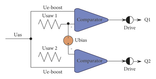
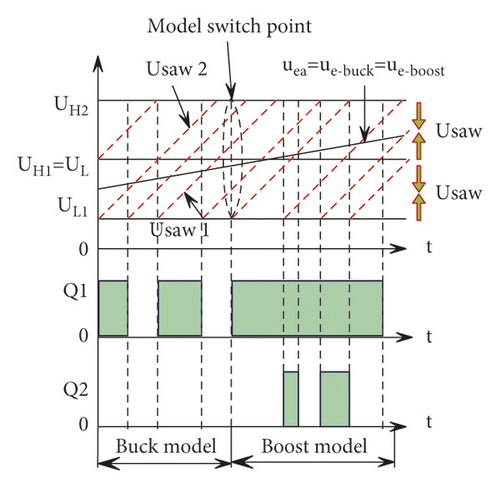
The typical control strategy of the two-mode control mode is single modulation signal-dual carrier two-mode control. As shown in Figure 1(a), in this method, the modulation signals of the switches Q1 and Q2 are the same; that is, uea = ue_buck = ue_boostuea = ue_buck = ue_boost. But the carrier signal usaw2 of Q2 is obtained by superimposing a DC component Ubias of the carrier signal usawl of Q1Q1; that is, usaw2 = usaw1 + Ubias. We set UL1 and UH1 to be the minimum and maximum values of usaw1 , respectively, and UL2 and UH2 to be the minimum and maximum values of usaw2, respectively. In order to ensure effective switching between the two working modes, UH1 − UL1 = UH2 − UL2 = Ubias = Usaw, where Usaw is the peak-to-peak value of the carrier signal, and the main working waveform is shown in Figure 1(b).
- (1)
When it is detected that |Uin − Uo| > ΔU (a constant, which can be set according to the actual situation), that is, when the power conversion circuit works in the non-pass-through mode, the control strategy is shown in Figure 2(a). Among them, the modulation signals of the switches Q1 and Q2 are the same; that is, uea = ue_buck = ue_boost, uea = ue_buck = ue_boost. But the carrier signal usaw2 of Q2 is obtained by superimposing a DC component Ubias of the carrier signal usawl of Q1Q1; that is, usaw2 = usawl + Ubias.
- (2)
Once it is detected that |Uin − Uo| = ΔU, that is, when the power conversion circuit enters the direct mode, the control strategy is shown in Figure 2(b); the switch Q1 is normally on and Q2 is normally off. At this time, the modulation signal uea remains unchanged at the previous moment and does not intersect with the carrier signal usaw, and the value of the current input voltage Uin needs to be recorded.
- (3)
When |Uin − Uo| ≤ ΔU, that is, when the power conversion circuit works in the pass-through mode, the modulation signal uea is always kept unchanged and does not intersect with the carrier signal usaw, and the input voltage Uin is detected in real time.
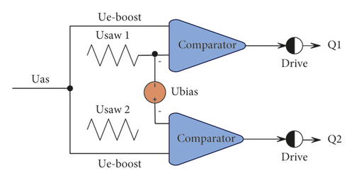
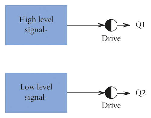
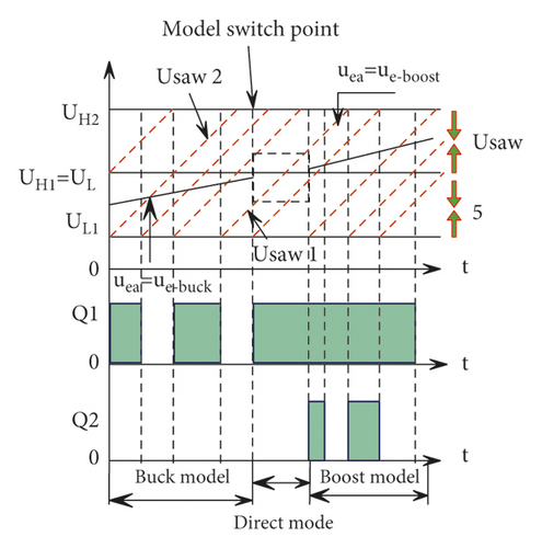
Once |U′in − Uin| > ΔU is detected, it indicates that the main circuit jumps out of the direct mode; that is, it enters the indirect mode. At this time, the modulation signal uea is re-interleaved with the carrier signal usaw to generate a pulse width modulation signal, and the control strategy changes from Figure 2(b) to Figure 2(a).
The main working waveform of the three-mode control mode is shown in Figure 2(c), where Usaw is the peak-to-peak value of the carrier signal.
To build an electronic circuit system model based on Saber simulation software, it is necessary to design and set the parameters of the power conversion circuit devices, and it mainly includes the parameter design and setting of the following related components.
2.3.1. Power Inductor
In the formula, IL(max), fs represent the maximum average value of the inductor current and the switching frequency, respectively. In the simulation practice, IL(max) = 6.95A,fs = 300 kHz are taken and substituted into (26), and the maximum value of L can be obtained as 71.11uH. Considering the 20% inductance margin, L is actually taken as 90uH.
2.3.2. Input Filter Capacitor
In the formula, I0(max), Po(max), fs represent the maximum output current, maximum output power, and switching frequency, respectively. In this design, Io(max) = 6.95A, Po(max) = 500W, fs = 300kHz are taken and substituted, and the maximum value of Cin can be obtained as 8.28uF. Considering the conventional 20% capacitance error value, Cin is actually taken as 11 uF (by 5 2.2 uF capacitors in parallel).
2.3.3. Output Filter Capacitor
In the formula, IL(max), fs represent the maximum value of average the inductor current and the switching frequency, respectively. In this design, IL(max) = 6.95A,fs = 300kHz are taken and substituted, and the maximum value of Co can be obtained as 33.1uF. Considering the conventional 20% capacitance error value, Co is actually taken as 44 uF (20 2.2 uF capacitors are connected in parallel).
2.3.4. Power Switch Tube
The power switches are divided into buck mode switches Q1 and boost mode switches Q2.
Since a certain type of aerospace electronic product is used, the switching frequency of the switch tube reaches 300 kHz, so that the switching loss accounts for most of the loss of the entire switch tube. Therefore, it is also necessary to choose a switching device with a shorter switching time.
2.3.5. Power Rectifier Tube
The power rectifier is divided into buck mode rectifier D1 and boost mode rectifier D2.
2.3.6. Current Sampling Resistor
In order to simulate the circuit state in the step-down working mode, a square wave input power supply is connected to the MOS transistor Q1 to keep Q1 in the state of the switch. By adjusting the duty ratio of the driving square wave signal of Q1, the output voltage of the power conversion main circuit can be changed. Since the MOS transistor Q2 is normally off during the buck step-down stage, a power supply with the voltage parameter set to 0 is connected to the MOS transistor Q2 to keep Q2 normally off. Here, the MOS transistor Q1 plays the role of chopping; that is, the DC input of the power conversion main circuit is chopped into a square wave, and the square wave can output a smooth DC voltage after passing through the LC (inductance, resistance) filter. The larger the duty cycle, the higher the average voltage of the square wave and the higher the output voltage.
In Figure 3, the role of the rectifier tube D1 composed of diodes Pwld1 and Pwld2 is to play a freewheeling role for the inductor L1. When Q1 changes from on to off, since the inductor current cannot change abruptly, a very high voltage will be generated, so a new inductor current path needs to be formed during this period to form the role of a freewheeling diode. The rectifier diode D2 composed of diodes Pwld3 and Pwld4 does not play a necessary role during this period, and the biggest function is to prevent the current output from flowing back.
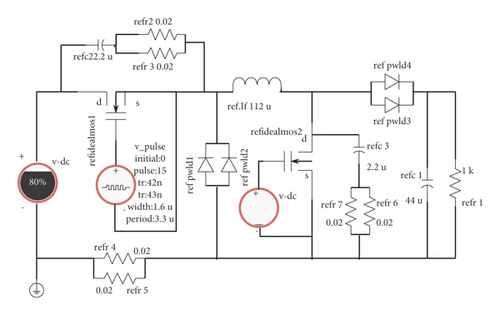
Figure 4 shows the Saber simulation of the power conversion main circuit of the dual-tube buck-boost topology in the boost mode. In the boost working mode, the MOS transistor Q1 is connected to a constant voltage source V3 with a voltage of 15 V and is kept normally open, while the MOS transistor Q2 is connected to a square wave pulse input power supply to maintain the switching state. The charging time of the inductor L can be controlled by controlling the driving duty ratio of the MOS transistor Q2 through the square wave pulse power supply. The longer the inductor charging time, the higher the output voltage. During simulation, the duty cycle changes when the frequency of the square wave supply changes, and the time it takes for the output voltage to reach steady state is reflected. The lower the frequency, the shorter the steady-state time, and the larger and more stable the output voltage.
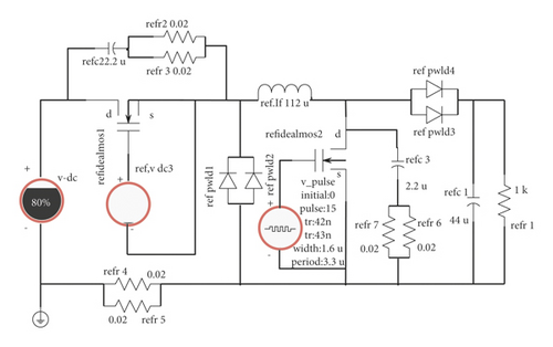
The rectifier diode D2 of the power conversion main circuit composed of diodes Pwld3 and Pwld4 prevents the output current from flowing back when the MOS transistor Q2 turns on the inductive energy storage device, and the output capacitor supplies energy to the load during this period. In the boost topology process, R6, R7, and capacitor C3 play the same role as R2, R3, and C2 to buffer and absorb voltage spikes to protect the MOS tube.
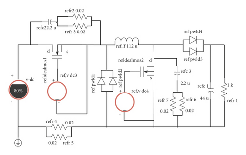
Figure 5 shows the Saber simulation under the straight-through mode of the dual-tube buck-boost power conversion main circuit. Under this mode control, the MOS transistor Q1 is connected to a 15 V constant voltage power supply to keep Q1 in the normally on state. The MOS tube Q2 is connected to a power supply whose voltage parameter is set to 0, which keeps Q2 normally off, so that the power conversion main circuit works in the direct mode. At this time, the absolute value of the difference between the input and output voltages remains constant.
3. Performance Optimization System of Electronic Components Based on Improved GA
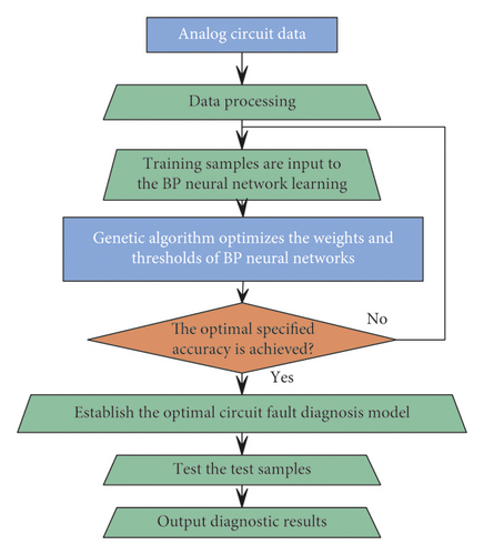
In this paper, the traditional GA is improved and applied to the performance optimization system of electronic components, and the results shown in Figure 6 are obtained.
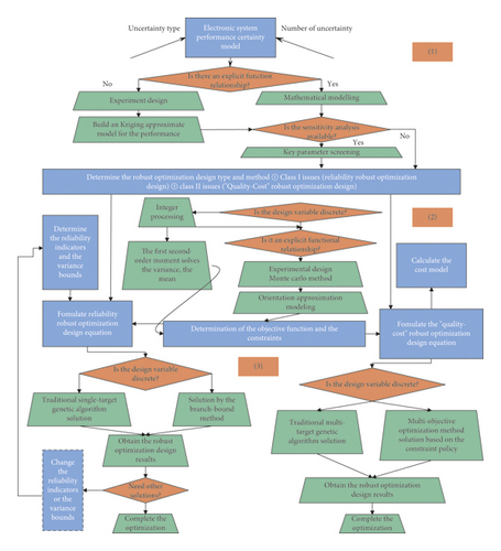
In the process of solving the robust optimization design of electronic systems, special attention should be paid to whether the design variables are in a discrete form and whether there is an explicit functional relationship between the performance response and the design variables. Figure 7 shows the complete robust optimization design implementation scheme.
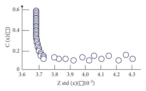
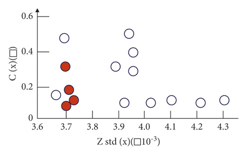
In order to further verify the effectiveness of the method in this paper, an improved multi-objective genetic algorithm is used for optimization, and the Pareto optimal solution set obtained by optimization is shown in Figure 8.
The effect evaluation of the electronic component performance optimization system based on the improved GA is carried out, and the evaluation results in Table 3 are obtained.
| Num | Performance boost | Num | Performance boost | Num | Performance boost |
|---|---|---|---|---|---|
| 1 | 80.803 | 15 | 85.684 | 29 | 84.846 |
| 2 | 81.874 | 16 | 83.026 | 30 | 83.425 |
| 3 | 80.881 | 17 | 83.403 | 31 | 80.943 |
| 4 | 86.546 | 18 | 81.920 | 32 | 80.130 |
| 5 | 84.401 | 19 | 82.094 | 33 | 83.319 |
| 6 | 86.605 | 20 | 85.243 | 34 | 84.585 |
| 7 | 83.048 | 21 | 85.309 | 35 | 83.571 |
| 8 | 81.539 | 22 | 84.287 | 36 | 80.419 |
| 9 | 81.764 | 23 | 82.921 | 37 | 86.963 |
| 10 | 81.506 | 24 | 86.663 | 38 | 81.309 |
| 11 | 85.016 | 25 | 86.093 | 39 | 85.705 |
| 12 | 83.398 | 26 | 84.843 | 40 | 80.073 |
| 13 | 80.277 | 27 | 84.905 | 41 | 85.088 |
| 14 | 86.180 | 28 | 82.828 | 42 | 80.311 |
It can be seen from the above research that the performance optimization system of electronic components based on the improved GA proposed in this paper has a certain effect on improving the performance of electronic components.
4. Conclusion
Complex large-scale equipment systems and electronic component production processes require a large number of multiparameter comprehensive measurements. Therefore, the research and application of distributed network testing technology have become a major trend. In the production and testing of electronic components, it involves the detection of a large number of process parameters and performance parameters. There are nearly 1,000 test parameters for various components used for testing. How to transmit and process such huge test data in real time puts forward extremely high requirements on the concurrency, real time performance, and data processing capability of the test platform. This paper uses the improved GA to construct the performance optimization system of electronic components to improve the performance of modern electronic components. The experimental research shows that the performance optimization system of electronic components based on the improved GA proposed in this paper has a certain effect on improving the performance of electronic components.
This paper studies the performance optimization of electronic components but does not consider the influence of environmental factors, such as temperature and humidity, on the performance of electronic components. Subsequent research can add these interference factors in practice to study the effect of the model.
Conflicts of Interest
The authors declare that there are no conflicts of interest.
Open Research
Data Availability
The labeled dataset used to support the findings of this study is available from the corresponding author upon request.


