An In Situ Spectral Monitoring Scheme for Advanced Manufacturing of Novel Nanodevices
Abstract
The advanced manufacturing of ultra-thin-film devices, especially the nano-semiconductor products, has drawn a significant research interest over the past decades. In this field, monitoring the properties and thickness of the semiconductor layers is of paramount importance, which has significant impact on the device quality. In this study, an in situ monitoring scheme for manufacturing of nanodevices has been proposed, which is able to accurately analyse the optical absorption properties of the semiconductor layers of varying thickness in nanodevices. The in situ reflectance spectral analysis of monolayer, bilayer, and bulk-phase samples confirms the practicability and reliability of the monitoring scheme. The findings reported in this study form the basis for the advanced manufacturing of nano- and sub-nanodevices in the future.
1. Introduction
The advanced manufacturing technologies have drawn a significant in recent years, including intelligent sensing, artificial intelligence, advanced monitoring, and other smart information technologies [1–6]. Owing to the critical role in advanced manufacturing, many researchers have attempted to exploit the opportunity of producing micro- and nanodevices in the past decades since the discovery of graphene in 2004 [7–10]. Particularly, the nanodevices based on two-dimensional (2D) materials have attracted great attention owing to their extraordinary properties, thus becoming the focus of research in the field of nanodevice manufacturing [11–16]. Considering material structure for nanodevices, the hybrid systems consisting of 2D and organic semiconductor thin films have sparked new research directions [17–21], and the combination of the advantages of both 2D and organic materials [22–24] has been widely considered to be promising for developing the novel nanodevices in the future. In recent years, the structures comprising van der Waals (vdW) epitaxial organic semiconductor films with controllable layers on the 2D material surface have emerged as one of the prime research highlights, as the properties and performance of the nanodevices based on such structures effectively correlate with the thickness of the organic layers [25–28]. Therefore, in order to satisfy the device functions and improve the production quality, a monitoring scheme, which is able to analyse the optical properties of thin films with different thicknesses, is essential for the advanced manufacturing of nano- and sub-nanodevices, especially the devices based on the structure of 2D/organic thin films which have been mentioned above.
2. Materials and Methods
2.1. Sample Preparation
The samples in this study consist of three materials from bottom to top: quartz (0001) substrate, h-BN film, and Me-PTCDI film. The samples have been prepared by using the following procedure:
Firstly, the h-BN thin film on the surface is prepared as follows:
Step 1. The pristine BN material is a single hexagonal bulk crystal. The bottom and top of a BN bulk piece are sandwiched between two pieces of tape, and the bulk is subsequently torn manually. At this stage, the BN bulk with a thickness about half of the original thickness is obtained.
Step 2. Step 1 is repeated several times until the h-BN thin film with the thickness at nanoscale is obtained gradually.
Step 3. The h-BN thin films are transferred onto the surface of an optical single crystal quartz (0001) substrate.
Secondly, the Me-PTCDI films with different numbers of layers are grown by van der Waals epitaxy on the h-BN/quartz substrate as follows [26]:
Step 1. The Me-PTCDI powder in a container is placed at the centre of the tube furnace, and the h-BN/quartz substrate is placed downstream at a suitable distance in the furnace.
Step 2. The tube is evacuated to 10-3 Pa.
Step 3. The Me-PTCDI powder is heated in the range 210-260°C to sublimate it, leading to the deposition on the h-BN surface. The process is continued until the film growth has been completed.
By controlling the factors such as the growing duration and the distance between the Me-PTCDI molecules and substrate, the Me-PTCDI thin films with varying number of layers are obtained successfully.
The optical microscope and photoluminescence (PL) images of a typical sample are shown in Figure 1.
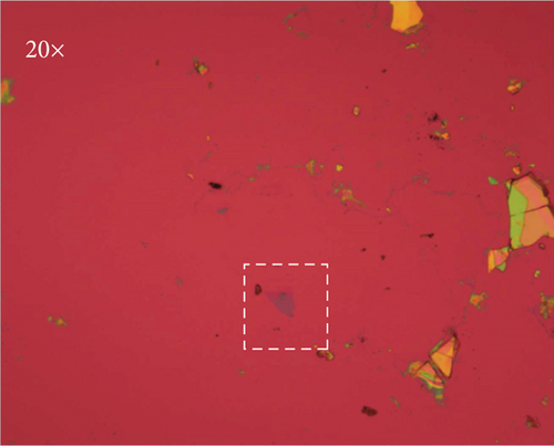
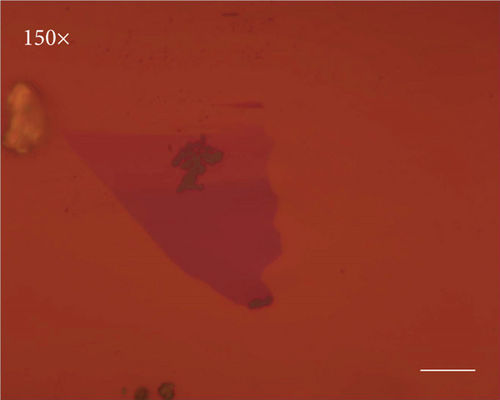
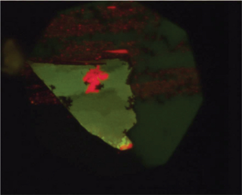
The optical analysis has been carried out by using an optical microscope (Olympus BX-51) using a 20x objective lens, followed by the zooming out of the area of interest by using a 150x objective lens. The optical microscopy images in Figure 1 reveal that the samples exhibit a small size in the range of several micrometres. The PL properties of the Me-PTCDI thin films of different thicknesses illuminated by a 450 nm LED are shown in Figure 1(c). The green fluorescence region represents the film formed by a monolayer of Me-PTCDI, whereas the red fluorescence region represents the film formed by more than one layer of Me-PTCDI [26].
Figure 1 demonstrates that it is inevitable that the Me-PTCDI films deposited on the h-BN surface remain uniform in such a microsize region. The mechanically exfoliated h-BN films are not only small but also random in size, shape, and surface quality. Besides, the deposition rates of the organic molecules on different areas are not the same. Therefore, the microarea DRS system with an ability to select the measuring region of any size and at any position is required.
2.2. Experimental Setup
The schematic illustration of the DRS system employed in this paper is presented in Figure 2. A brief introduction of the experimental system is given as follows.
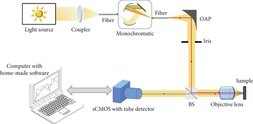
In order to cover the range of the characteristic peaks of the organic molecules, which are always in the visible wavelength band, a 75 W Super-Quiet Xenon-lamp (Hamamatsu) has been used as the light source. A fiber coupler is utilized between the lamp and optical fiber to avoid the loss of intensity as much as possible. A monochromatic (SP2150, Princeton Instrument) with a grating flash at 500 nm has been used to obtain the single wavelength light. The off axis parabolic mirror (OAP, Thorlabs) functions as a collimator. The iris and the 50R/50 T beam splitter (BS, produced by Thorlabs) are placed before the 20x objective lens (Nikon CFI 60 TU Plan Epi). To match the light source with high intensity, a deep well miniature sCMOS camera (Panda 4.2 PCO) with a 200 mm tube lens (Edmund) is utilized as the detector, employed simultaneously with homemade software for spectral acquisition and recording.
2.3. Measurement Methods
The measurement methods consist of the three steps: acquisition of spectral signal, selection of measurement area, and the calculation of DRS, which are described in detail as follows.
2.3.1. Step 1: Acquisition of Spectral Signals
The steps for spectral signal acquisition are illustrated in Figure 3. The experimental parameters, including the start and end wavelength of the spectral detection range, step wavelength of the monochromator, exposure duration, and average times of a single acquisition, have been set according to the experimental requirements prior to the measurements. The reflected light intensity of the signals at all wavelengths is subsequently recorded.

2.3.2. Step 2: Selection of the Area of Measurement
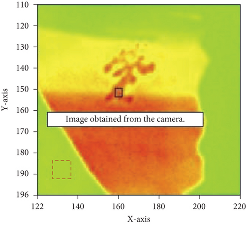
The reflected intensity images at single wavelengths are imported into the computer by using the homemade software. Subsequently, the images are employed to select the measurement area. For instance, the image at 550 nm wavelength is used to select the measurement area, which has been shown in Figure 4. The range of the black solid rectangle is selected as the area covered by the Me-PTCDI film, and the range of the red dashed rectangle is selected as the substrate. The rectangular area is taken for example here. In fact, the selected area can be of any shape and size, even a single pixel.
2.3.3. Step 3: Calculation of DRS
The average reflected intensities of the experimental wavelengths from the selected area are calculated automatically by using the homemade software. Afterwards, the calculated average intensities for each wavelength from the sample area and substrate are incorporated into equation (1) as I (E, d) and I (E, 0), respectively, to carry out the DRS analysis.
3. Experiments and Discussion
3.1. Absorption Characteristics of the Monolayer Me-PTCDI Film on the h-BN Surface
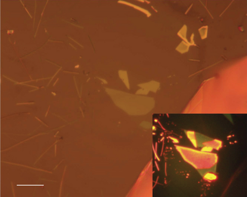
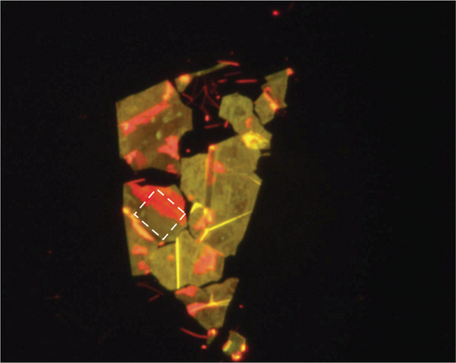
The optical microscopy and PL image of the sample including monolayer Me-PTCDI films are shown in Figure 5. Based on the PL characteristics of the Me-PTCDI film, the green fluorescence region can be confirmed as the monolayer, whereas the red fluorescence region represents the area covered with more than one layer of the Me-PTCDI molecules. In order to analyse the characteristics of the monolayer film, the samples are measured at room temperature by using the microarea DRS system proposed in this paper. The reflected intensities from the green area representing the monolayer Me-PTCDI on h-BN and the black area representing the quartz substrate are utilized as the signals of the monolayer film and substrate, respectively, to calculate DRS. The absorption of h-BN is noted to be out of the range of experimental wavelengths; thus, the peaks in Figure 6 correspond to the characteristics of the Me-PTCDI monolayer.
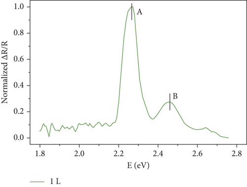
Two peaks of the S0-S1 transition vibronic levels have been observed in the monolayer films. Peak A is observed at 2.26 eV whereas peak B is located at 2.46 eV. The positions of the two peaks are observed to be consistent with the characteristics of the Me-PTCDI monolayer film in the report earlier [26]. It proves that the microarea DRS system proposed in this paper is able to realize the spectral resolution at the monolayer level, even though the measuring area is extremely small, and the reflected intensity is relatively weak.
In addition, by comparing the position of the two peaks with those of the monomer in solution at room temperature [51], it can be observed that both peaks in the monolayer exhibit the redshift from the monomer. The redshift phenomena demonstrate that the first layer of the Me-PTCDI deposited on the h-BN substrate has assembled to form the J-aggregate, which has been extensively studied for novel applications [55–57]. It indicates that the structure based on the Me-PTCDI monolayer and h-BN is suitable for producing the sub-nano-thin-film devices.
3.2. Absorption Characteristics of the Me-PTCDI Bilayers on the h-BN Surface
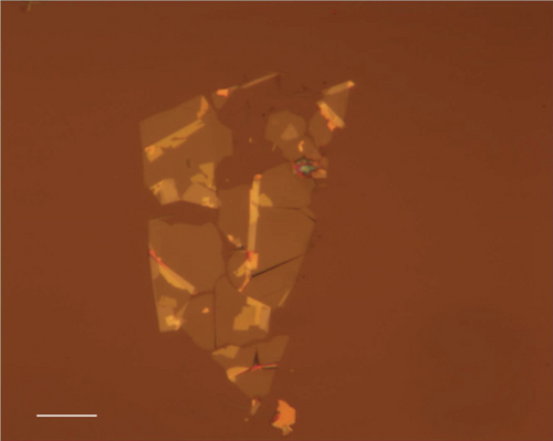
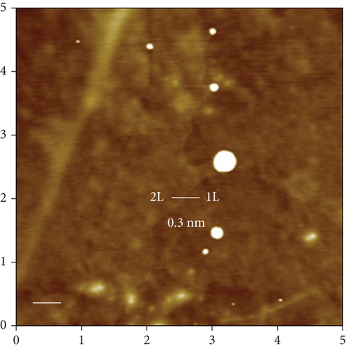
The optical atomic force microscopy (AFM) images of the sample are shown in Figure 7. The measuring area of the monolayer film can be determined based on the PL image in Figure 7(b). According to the thickness of the monolayer film of Me-PTCDI on h-BN of about 0.3 nm [26], the area with a step of 0.3 nm from the monolayer region can be identified as bilayers in the AFM (Oxford Instruments Asylum Cypher) image. In addition, the DRS signals of the monolayer and bilayers in the area demonstrated in Figure 7(c) are shown in Figure 8.
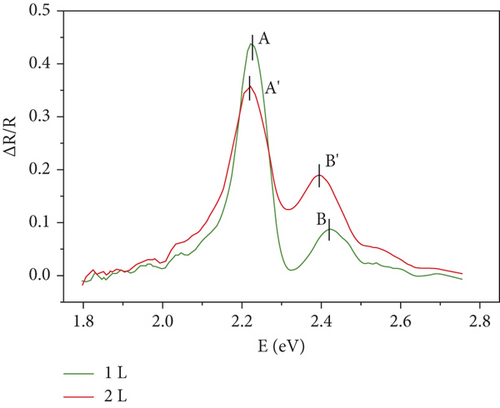
It can be observed that the both characteristics peaks in the bilayers (peak A ′ at 2.18 eV and peak B ′ at 2.40 eV) have been slightly redshifted as compared to the monolayer, which usually occurs during the film growth. However, the abnormal absorption has been observed that the intensity of peak B has increased while the intensity of peak A is decreased, although more molecules exist in the bilayer films.
The phenomenon is likely attributed to the influence of the different molecular aggregates in the Me-PTCDI monolayer and bilayer films. The Me-PTCDI monolayer films solely consist of the J-aggregates, formed by the head-to-tail orientation of the molecules on the surface. It is negative to the excitonic coupling, and the intensity of the spectral peaks is mostly generated by the Frenkel exciton (FE) transition. On the other hand, in bilayers, the H-aggregates formed by the molecules depicting the side-by-side orientation are noted to appear. It is positive to the excitonic coupling between the molecules, thereby resulting in the charge transfer (CT) transition, which has a narrower band gap and more easily realized transition behaviours as compared with FE. Thus, the slight redshifting of the peaks is attributed to the excitonic coupling in bilayers. Furthermore, once the second layer is deposited on the monolayer, a growing number of Me-PTCDI molecules enhance the absorption; however, the interaction generated by the H-aggregates represses the FE transition which has taken place in the monolayer. In addition, for the peaks at different energy positions, the two absorbing species function differently. For some typical organic thin films, the lowest excited state is almost pure FE exciton, whereas mixing between the FE and CT excitons occurs in the region of its vibronic replicas at higher energy positions [51].
Therefore, the experimental results indicate that for the lowest absorption transition contributing to peak A, the FE in the Me-PTCDI monolayer is so significant that the repression of the FE transition results in a decline in the absorption, although additional molecules exist in the bilayers. This observed DRS result also confirms the giant oscillator strength of the Me-PTCDI monolayer film reported in literature [26]. On the other hand, for peak B, which is the vibronic replica of peak A, the enhanced absorption generated by CT in bilayers dominates the characteristic behaviour, which represents an equilibrium between the two exciton species. Actually, the interesting phenomena have also been observed and investigated for the 3,4,9,10-perylenetetracarboxylic dianhydride (PTCDA) thin films [31–33], which is very similar to Me-PTCDI.
The experimental results prove the performance and reliability of the microarea DRS scheme, along with providing insights for producing devices, where the monolayer photoelectric devices based on ultrathin Me-PTCDI must exhibit a better performance at the sub-nanoscale as compared to the bilayer-based devices.
3.3. Absorption Characteristics of the Bulk-Phase Me-PTCDI Film on the h-BN Surface
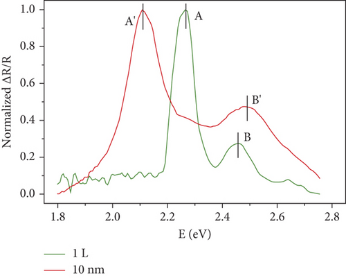
The multilayers of Me-PTCDI thin films have also been deposited on other areas of the sample in Figure 5. Combining the AFM topography in Figure 9 with the PL image in Figure 5, the target areas of the multilayer films with different thicknesses can be selected. The DRS and normalized DRS results of the areas with different monolayers and thicknesses of 6 nm and 10 nm are illustrated in Figure 10.
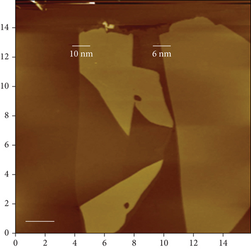
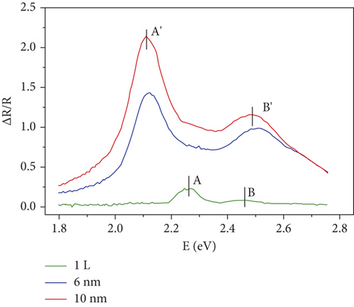
The DRS signals for the sample films with monolayer (green curve), 6 nm (blue curve), and 10 nm (red curve) thicknesses are shown in Figure 10(a). Comparing the curves with different thicknesses, it is obvious that the absorption of the films increases with the thickness owing to the availability of an enhanced extent of molecules to absorb photons.
As shown in Figure 10(a), the positions of the two characteristic peaks (peak A ′ at 2.10 eV and peak B ′ at 2.48 eV) in the case of 6 nm and 10 nm films are almost the same, exhibiting independence on the film thickness. Therefore, such films can be regarded as the bulk-phase films.
To analyse the differences between the monolayer and bulk-phase films more effectively, the normalized DRS of the monolayer and 10 nm films is shown in Figure 10(b). The interesting phenomena of peak broadening and peak shift are described in the following.
By comparing the peak width of the bulk-phase film with the monolayer, the broadening phenomena have been observed apparently. The peaks observed in the case of the monolayer film are mostly attributed to FE, which results in the narrow peaks, while the coupling between the layers in bulk-phase films contributes to different excitons (such as FE, CT, and FE-CT) with different energy positions, which results in peak broadening. In addition, the scattering between the excitons and phonons in the thicker films at room temperature also contributes to peak broadening.
Furthermore, it is interesting to note that peak A has been redshifted from the monolayer to the bulk phase, while peak B has been blueshifted. It is likely due to the impact of the substrate described as follows.
In the monolayer film, the π-π conjugation is not formed among the molecules owing to the molecular J-aggregates, while in the bulk-phase films consisting of both J-aggregates and H-aggregates, the π-π bond can be formed between the adjacent layers of molecules. It leads to the electronic coupling, which leads to that the Coulomb potential of molecules has been decreased. Therefore, the characteristic peaks of the multilayer films must move to the lower energy positions in case the interaction among the molecules functions alone.
However, the Coulomb potential between h-BN and Me-PTCDI is different from the Coulomb energy among the Me-PTCDI molecules, also affecting the excitonic transition at the same time. It is commonly reported that the initial layers (especially the first layer) of the organic film are influenced by the substrate significantly, while the impact decreases in the subsequent molecular layers. As a result, the films tend to become stable and form a bulk phase gradually [33–37].
Therefore, the peak shifting from the monolayer to bulk crystal is the combination of the two kinds of different Coulomb energy interactions mentioned above. With respect to the different peak shift phenomena, it is likely that the interaction between the h-BN substrate and Me-PTCDI contributes to locating the peaks in the monolayer to a lower energy position, but the impact degrees of substrate on the two characteristic peaks are different. For the lowest exited transition (peak A and peak A ′), the impact of the h-BN substrate is weaker than the effect of Me-PTCDI molecular layers; thus, peak A has been redshifted to peak A ′ from the monolayer to bulk phase, while for the vibronic replicas of the lowest transition (peak B and peak B ′), the impact of the substrate is more significant than the effect of molecules so that peak B in the monolayer is located at a rather lower energy positon as compared to peak B ′ in bulk crystal, which results in the blueshift phenomena.
The experimental results demonstrate that the microarea DRS scheme is practical at both sub-nano- and nanoscales. Also, the important information for producing devices is revealed that the substrate influences the performance of ultrathin films devices apparently and the devices based on bulk crystal Me-PTCDI must function differently as compared to the devices based on the monolayer films.
4. Conclusions
In this paper, an in situ microarea DRS scheme has been applied to investigate the dependence of the absorption properties on the thickness of the Me-PTCDI films on the h-BN surface, which is a typical structure contained in the nanodevices. The experimental results obtained in this study demonstrate the successful application of the scheme to the monolayer level.
The optical performance of the monolayer, bilayers, and bulk phase of the Me-PTCDI films on the h-BN surface has been analysed by using microarea DRS. Several interesting phenomena and critical properties of the Me-PTCDI/h-BN structure have been revealed. It is demonstrated that the ultrathin Me-PTCDI films on h-BN can be utilized for the sub-nanophotoelectric devices. In particular, the performance of the monolayer device is noted to be superior owing to its greater absorption. In addition, the substrate material for the monolayer devices is also vital due to its significant impact on the monolayer absorption. Furthermore, for the devices produced by incorporating the bulk phase Me-PTCDI films on h-BN at the nanoscale, the performance based on absorption properties can be improved by increasing film thickness, which will function at different characteristic wavelengths with a wider band as compared to the monolayer devices.
The findings reported in this study prove that the microarea DRS scheme is able to detect and analyse the thickness and optical properties of the ultrathin films in the nano- and sub-nanodevices. The scheme is practical and potentially promoted for advanced manufacturing of the nano-thin-film devices in the future.
Conflicts of Interest
The authors declare they have no competing interests.
Acknowledgments
This work was supported by the National Key Research and Development Program of China (No. 2017YFF0107003). Thanks are due to Dr. Huijuan Zhao for the help in samples, and thanks are due to Dr. Hongxiang Zhang for the help in experimental discussion.
Open Research
Data Availability
All data used to support the findings of this study are included within the article.


