Characteristics of Metal–Semiconductor–Metal Ultraviolet Photodetectors Based on Pure ZnO/Amorphous IGZO Thin-Film Structures
Abstract
In this study, metal–semiconductor–metal-structured ultraviolet (UV) photodetectors (PDs) based on pure zinc oxide (ZnO) and amorphous indium gallium zinc oxide (a-IGZO) thin films were fabricated and characterized. The ZnO seed layers were deposited on Corning glass substrates via a radio frequency (RF) magnetron sputtering technique. Results showed that under a 5 V applied bias; the dark currents of the pure ZnO and a-IGZO thin films were 0.112 pA and 2.85 nA, respectively. Meanwhile, the UV-to-visible rejection ratio of the pure ZnO and a-IGZO thin films were 14.33 and 256, respectively. Lastly, the PDs of thea-IGZO thin films had a lower leakage current and higher rejection ratio than that of the pure ZnO thin films from the UV to visible light region.
1. Introduction
In recent years, ultraviolet (UV) photodetectors (PDs) have played an important role in human health, ozone layer monitoring, and flame detection [1, 2]. Zinc oxide (ZnO) is a novel metal oxide semiconductor material that is used as an integral part of UV PDs [3, 4]. ZnO is an n-type and II-VI material; its bandgap is approximately 3.37 eV, and its excitation binding energy is 60 meV at room temperature [5, 6]. ZnO is a good crystallinity material. It has a hexagonal structure, and the lattice constants are a = 3.24–3.26 Å and c = 5.13–5.43 Å [7–9]. In addition, the lowest surface free energy of ZnO thin films lies on the (002) plane, and a good c-axis orientation can be obtained at a low temperature when ZnO thin films are grown. In addition to having good carrier mobility and photoelectric properties, crystalline metal oxide semiconductors are amorphous oxide semiconductor materials and thus have attracted considerable attention; moreover, the inclusion of ZnO compounds has led to extensive research. The type of material consists of various transition metals and oxygen atoms, such as zinc tin oxide (ZnSnO) [10], indium zinc oxide (InZnO) [11], and indium gallium zinc oxide (InGaZnO) [12], to enhance overall carrier mobility and photoelectric properties. Among them, the InGaZnO (IGZO) is a ternary oxide semiconductor. Its composition includes In2O3, Ga2O3, and ZnO. Amorphous IGZO oxide semiconductors have high carrier mobility, good uniformity, and wide energy bandgap, which offers good transparency in the visible spectrum; its peculiar chemical bonding instigates high field mobility and displays improved electrical characteristics, such as high ION/IOFF ratio, enhanced lifetime, improved transmittance, and optimum large-area uniform integration [13–15]. The characteristics of transparency can be applied to the optical field.
In this study, the difference between crystalline ZnO thin-film PDs and amorphous IGZO thin-film PDs is discussed.
2. Experimental
Before UV PDs were manufactured, 1 cm × 1 cm Corning glass substrates were, respectively, cleaned for 10 min with acetone, isopropyl alcohol, and deionized water in an ultrasonic cleaner. Afterward, they were dried with flowing nitrogen and then placed in an oven for approximately 10 min at 45°C. Three-inch-diameter targets of pure ZnO and a-IGZO (atomic ratio In : Ga : Zn = 1 : 1 : 1) with a purity of 99.99% were used. The pure ZnO and a-IGZO thin films were grown using the radio frequency magnetron sputtering technique under a sputtering power of 100 W, a gas mixing ratio of Ar/O2 (10/1), and a maintained chamber pressure at 5 × 10⁻² Torr. The thickness was approximately 40 nm. Afterward, the film was annealed in a vacuum furnace at 450°C for 1 h to improve crystal quality. The resistivity of the pure ZnO thin films was ~10−5 (ohm-cm), and that of the a-IGZO thin films is approximately 1 × 10⁻³ (ohm-cm). The surface morphology, surface roughness, and crystallographic of the pure ZnO and a-IGZO thin films were characterized and explored by field-emission scanning electron microscopy (FE-SEM, JEOL JSM-6700F), atomic force microscopy (AFM, NT-MDT), and X-ray diffraction spectrum analysis with Cu Kα-1 radiation and λ = 0.15405 nm (XRD, MO3XHF22 MAC-Science), respectively. The optical characteristic was measured using a UV/visible spectrometer (UV-VIS, Hitachi U-2800).
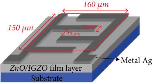
In part of devices, the standard photolithography and lift-off were then performed to define the interdigitated (IDT) mask region. The IDT electrode measured 146, 10, and 10 μmin length, width, and space, respectively. The sensing active region was 150 μm × 160 μm. Subsequently, the silver (Ag) electrode was deposited by e-gun evaporation and used as contact electrode to form a metal–semiconductor–metal (MSM) structure, as shown in Figures 1(a) and 1(b). The light and dark currents of MSM UV PDs were measured by a semiconductor parameter analyzer (Agilent HP 4156C) system. The photoresponse was measured by a light source, i.e., a 300 W Xe lamp and a monochromator, from a 300–600 nm range. In this work, two MSM UV PD devices were fabricated to identify which is better.

3. Results and Discussion
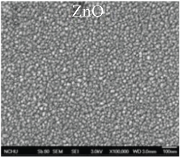
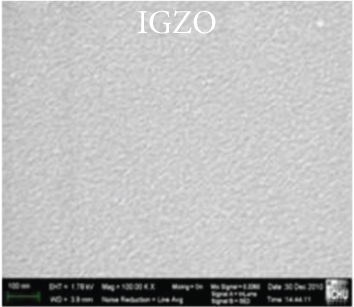
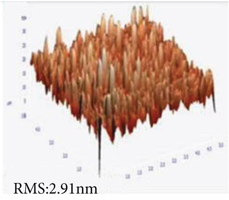
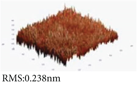
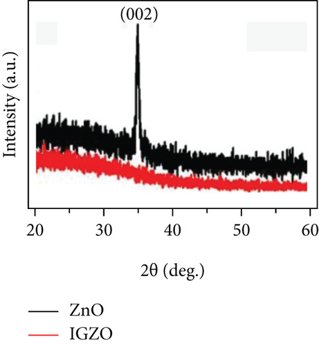
Figures 2(a) and 2(b) show the surface morphology of pure ZnO and a-IGZO thin films by FE-SEM analysis and clearly indicate the difference between the surfaces of pure ZnO and a-IGZO. The pure ZnO film underwent grain formation, whereas the a-IGZO film did not. According to the AFM images shown in Figures 2(c) and 2(d), the surface roughness RMS value of the ZnO film was 2.91 nm, and that of the a-IGZO film was 0.238 nm, indicating that the overall surface of the pure ZnO film was rougher than the a-IGZO film because of grain formation. Figure 2(e) depicts the typical XRD results of the pure ZnO NRs and a-IGZO thin films that were prepared on the Corning glass substrate. The results indicated that the diffraction peak corresponded with the (002) planes. The peak revealed the hexagonal wurtzite structure of ZnO (JCPDS Card No. 36-1451) [16]. On the contrary, IGZO films showed amorphous phenomena [17].
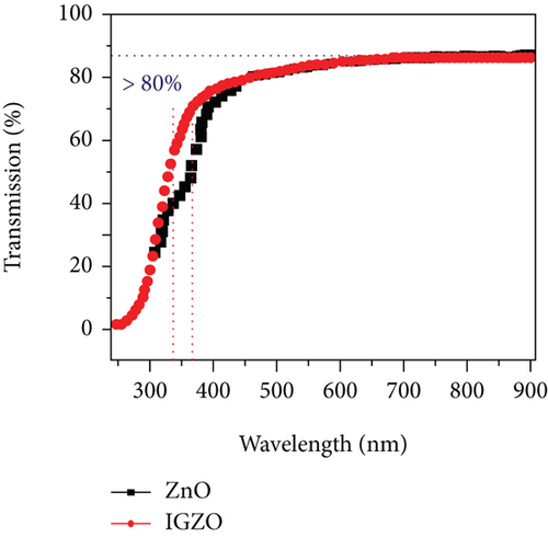
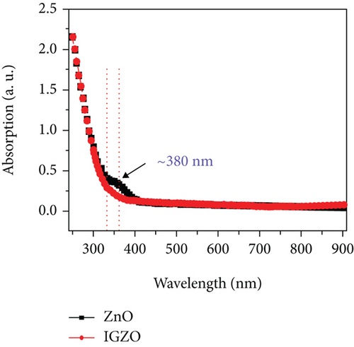
Figures 3(a) and 3(b) show the spectrum of transmission and absorption of pure ZnO and a-IGZO thin films. Both had the same thickness of thin films, and the transmission could reach approximately 80% in the visible wavelength [18, 19]. However, the main difference was that the pure ZnO thin films slightly decayed in the 300–400 nm wavelengths. In the absorption spectrum, the absorption of the a-IGZO thin films was deeper than that of the pure ZnO thin films.
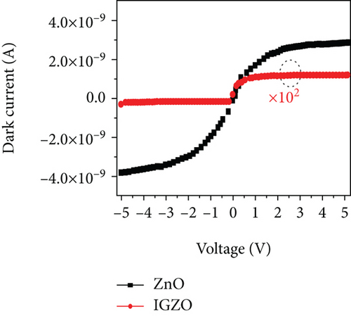
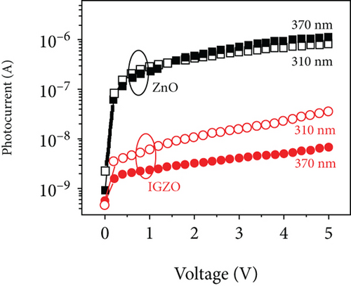
| Current (A) | Pure ZnO | a-IGZO |
|---|---|---|
| Idark | 2.85 nA | 0.112 pA |
| Iph(310 nm) | 0.82 μA | 36.3 nA |
| Iph(370 nm) | 1.1 μA | 6.6 nA |
| Iph(ZnO)/Idark(ZnO)(370 nm) | 385.9 | |
| Iph(IGZO)/Idark(IGZO)(370 nm) | 589.2 | |
| Iph(ZnO)/Iph(IGZO)(310 nm) | 22.53 | |
| Iph(ZnO)/Iph(IGZO)(370 nm) | 166.6 | |
where q is the electronic charge, η is the quantum efficiency, A is the active area, Фph is the photon flux, and G is the photoconductive gain. The ratio of light current to dark current Iph/Idark was 589.2 in a-IGZO and 385.9 in pure ZnO; the former was larger than the latter. In addition, the photocurrent of the pure ZnO films was larger than the a-IGZO thin films, that is, approximately 166.6 times of Iph(ZnO)/Iph(IGZO).
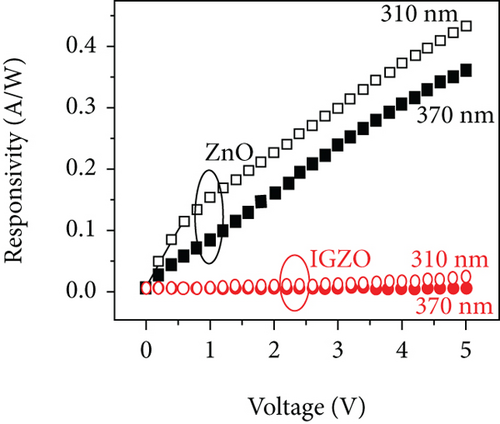
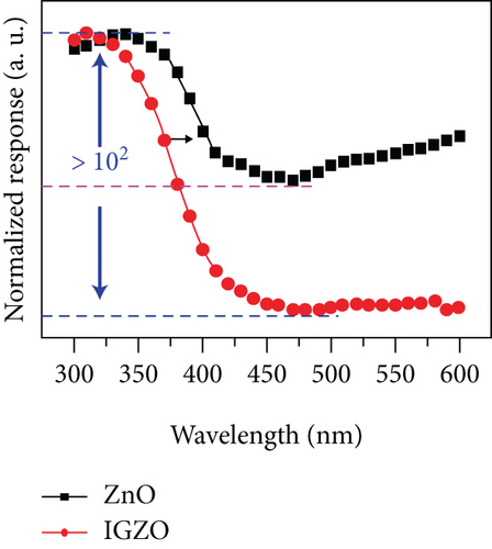
| Responsivity (R) | Pure ZnO/a-IGZO |
|---|---|
| R310 nm(ZnO)/R370 nm(ZnO) | 1.22 |
| R310 nm(IGZO)/R370 nm(IGZO) | 10 |
| R310 nm(ZnO)/R450 nm(ZnO) | 14.33 |
| R310 nm(IGZO)/R450 nm(IGZO) | 256 |
where Idark is the dark current, Ilight is the photocurrent, and Popt is the incident optical power. The UV-to-visible rejection ratio of a-IGZO PD ([R310nm (IGZO)/R450nm (IGZO)] = 256) was larger than that of pure ZnOPD ([R310nm(ZnO)/R450nm(ZnO)] = 14.33); in addition, the absorbance of UV light in the a-IGZO was deeper at a 310 nm wavelength.
4. Conclusion
The MSM structure of UVPDs based on pure ZnO and a-IGZO thin films was fabricated and characterized. Results showed that the dark currents of the pure ZnO and a-IGZO thin films were 0.112 pA and 2.85 nA, respectively, under a 5 V applied bias. Meanwhile, the UV-to-visible rejection ratios of the pure ZnO and a-IGZO thin film were 14.33 and 256, respectively. In the pure ZnO thin films, the dark current was evident under the transmission path of grain boundaries. Therefore, the dark current and photocurrent became larger. This result indicated that the dark current could be restrained by an amorphous morphology. Lastly, the PDs of the a-IGZO thin films had a lower leakage current and higher rejection ratio than that of the pure ZnO thin films from the UV to visible light region. In the future technology, the UV PDs can be combined with the Internet of Things and applied it to human skin to avoid skin aging and skin cancer.
Conflicts of Interest
The authors declare there are no competing interests.
Authors’ Contributions
Yen-Lin Chu and Chi-Nan Tsai performed the experiments; Kin-Tak Lam, Sheng-Joue Young, and Liang-Wen Ji conceived the experiments; Tung-Te Chu and Ting-SungLu participated in data analysis.
Acknowledgments
This work was financially supported by the Ministry of Science and Technology of Taiwan (Project numbers MOST 107-2221-E-150-032, MOST 108-2221-E-024-006, MOST 108-2221-E-150-013-MY2, MOST109-2221-E-239-031-MY2, and MOST 106-2221-E-239-037-MY3). The authors would like to thank the Common Laboratory for Micro/Nano Science and Technology of the National Formosa University for the use of their measurement equipment and their assistance in this work; the Center for Micro/NanoScience and Technology, National Cheng Kung University, for device characterization; and C. N. Tsai for device fabrication and equipment support.
Open Research
Data Availability
All the data results in our article, we can provide them if requested.


