Defected Ground Structure: Fundamentals, Analysis, and Applications in Modern Wireless Trends
Abstract
Slots or defects integrated on the ground plane of microwave planar circuits are referred to as Defected Ground Structure. DGS is adopted as an emerging technique for improving the various parameters of microwave circuits, that is, narrow bandwidth, cross-polarization, low gain, and so forth. This paper presents an introduction and evolution of DGS and how DGS is different from former technologies: PBG and EBG. A basic concept behind the DGS technology and several theoretical techniques for analysing the Defected Ground Structure are discussed. Several applications of DGS in the field of filters, planar waveguides, amplifiers, and antennas are presented.
1. Introduction
Conventional microstrip antennas had some limitations, that is, single operating frequency, low impedance bandwidth, low gain, larger size, and polarization problems. There are number of techniques which have been reported for enhancing the parameters of conventional microstrip antennas, that is, using stacking, different feeding techniques, Frequency Selective Surfaces (FSS), Electromagnetic Band Gap (EBG), Photonic Band Gap (PBG), Metamaterial, and so forth. Microwave component with Defected Ground Structure (DGS) has been gained popularity among all the techniques reported for enhancing the parameters due to its simple structural design. Etched slots or defects on the ground plane of microstrip circuits are referred to as Defected Ground Structure. Single or multiple defects on the ground plane may be considered as DGS. Initially DGS was reported for filters underneath the microstrip line. DGS has been used underneath the microstrip line to achieve band-stop characteristics and to suppress higher mode harmonics and mutual coupling. After successful implementation of DGS in the field of filters, nowadays DGS is in demand extensively for various applications. This paper presents the evolution and development of DGS. The basic concepts, working principles, and equivalent models of different shapes of DGS are presented. DGS has been used in the field of microstrip antennas for enhancing the bandwidth and gain of microstrip antenna and to suppress the higher mode harmonics, mutual coupling between adjacent element, and cross-polarization for improving the radiation characteristics of the microstrip antenna. Applications of DGS in microwave technology are summarized in this paper and the applications of DGS in the field of antennas are discussed.
Low cost, high performance, compact size, wideband, and low profile antennas often meet the stringent requirements of modern wireless communication systems. Modern communication demands the availability of efficient, compact, and portable devices that can be operated at high data-rates and at low signal powers. Researchers have been working towards the development and advancement of RF front ends to meet the latest requirements. Various novel approaches have been reported to improve the performance of microwave component. PBG has been proposed by John and Yablonovitch proposed [1, 2]. For providing a rejection band of certain frequency PBG is used. Periodic structure on the ground plane provides a rejection band. However, the modelling of PBG structure for microwave and millimeter-wave components is very difficult. Radiation from periodic etched defects, number of lattice, lattice shapes, lattice spacing and relative volume fraction are some parameters that effects the band gap properties of PBG. There is another ground plane aperture (GPA) technique, which simply incorporates the microstrip line embedded with a centred slot at the ground plane. GPA has been reported for 3 dB edge coupler and bandpass filters [3–5]. Width of the GPA creates a significant effect on the characteristic impedance of the microstrip line, hence controlling the return loss level.
In order to alleviate these problems, Park et al. [6] proposed Defected Ground Structure (DGS) firstly and used the term “DGS” in describing a single dumbbell shaped defect. The DGS can be regarded as a simplified form of EBG structure, which also exhibits a band-stop property [7]. DGS opens a door to microwave researchers of a wide range of applications. Various novel DGSs have been proposed and lot of applications have been explored extensively in microwave circuits. The development of DGS is thoroughly discussed in [8]. Subsequently, three books [9–11] have addressed the microstrip antennas with DGS. DGS has become an alternative of EBG for modern applications due to its simplicity and low cost. Dumbbell shaped DGS was initially used to realize a filter [12], and other shapes were reported subsequently to realize different microwave circuits such as filters [13–20], amplifiers [21], rat race couplers [22], branch line couplers, and Wilkinson power dividers [23, 24]. In [25], the DGS is integrated with a MPA. Deferent DGS printed antennas have been investigated in [8].
In this paper, an overview and evolution of DGS are presented in detail. The working principles and basic concepts of DGS units are introduced and the equivalent circuit models of DGS units available in literature are also presented. In the last section, the applications of DGS in modern wireless communication are presented and the evolution trend of DGS is given.
2. Photonic Band Gap
Photonic Band Gap (PBG) structures are periodic structures etched on the ground plane and have the ability to control the propagation of electromagnetic waves. Periodic structures effects the current distribution of the structure. The periodic structures can influence on the propagation of electromagnetic waves and radiation characteristics. The PBG have the periodic defects, which can be treated as a resonant cavity and affect the propagation of the electromagnetic waves. PBG forms free mode inside the forbidden band gap and provides a stopband at certain frequency. PBG has been reported for improving the directivity of antennas, surface wave’s suppression, and harmonics suppression [26].
3. Electromagnetic Band Gap (EBG) Structure
The EBG technique is based on the PBG phenomena and also realized by periodical structures. In [27], EBG has been introduced as high-impedance surface or PBG surface. These structures are compact and result in high gain, low profile and high efficiency antennas. EBG has been created an interest in the field of antenna. EBG structures suppress the surface wave current hence increase the antenna efficiency. The surface waves decrease the antenna efficiency. Surface wave suppression using EBG technique improves the antenna performance by increasing the antenna efficiency and antenna gain [28].
4. Defected Ground Structure
The compact geometrical slots embedded on the ground plane of microwave circuits are referred to as Defected Ground Structure (DGS). A single defect (unit cell) or a number of periodic and aperiodic defects configurations may be comprised in DGS. Thus, periodic and/or aperiodic defects etched on the ground plane of planar microwave circuits are referred to as DGS. Earlier Photonic Band Gap (PBG) [26] and Electromagnetic Band Gap (EBG) [27, 28] have been reported with irregular ground planes. The comparison between PBG, EBG, and DGS is depicted in Table 1.
| PBG | EBG | DGS | |
|---|---|---|---|
| Definition | Photonic Band Gap (PBG) structures are periodic structures etched on the ground plane and have the ability to control the propagation of electromagnetic waves | The EBG technique is based on the PBG phenomena and also realized by periodical structures but compact in size | Single or few compact geometrical slots embedded on the ground plane of microwave circuits are referred to as Defected Ground Structure (DGS) |
| Geometry | Periodic etched structure | Periodic etched structure | One or few etched structures |
| Parameter extraction | Very difficult | Very difficult | Relatively simple |
| Size | Large | Smaller than PBG and larger than DGS | Much more compact than PBG and EBG |
| Fabrication | Difficult | Difficult | Easy |
| Examples | [26] | [27, 28] | [12–24] |
4.1. Working Principle
DGS has been integrated on the ground plane with planar transmission line, that is, microstrip line, coplanar waveguide, and conductor backed coplanar wave guide [12–24]. The defects on the ground plane disturb the current distribution of the ground plane; this disturbance changes the characteristics of a transmission line (or any structure) by including some parameters (slot resistance, slot capacitance, and slot inductance) to the line parameters (line resistance, line capacitance, and line inductance). In other words, any defect etched in the ground plane under the microstrip line changes the effective capacitance and inductance of microstrip line by adding slot resistance, capacitance, and inductance.
4.2. Unit DGS
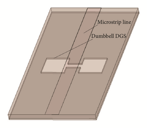
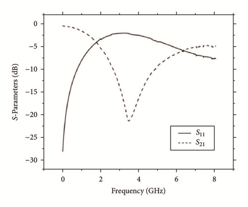
The first DGS model has been reported as a dumbbell shaped defect embedded on the ground plane underneath the microstrip as shown in Figure 1 [12]. The response of its return loss is also shown in the figure.
DGS has some advantages over PBG. (1) In PBG, periodic structures occupy a large area on the circuit board. On the other hand a few DGS elements may create similar typical properties. Hence, circuit size becomes compact by introducing DGS. (2) DGS is comparably easy to design and fabricate and its equivalent circuit is easy to realize. (3) Higher precisions are achieved in comparison to other defect embedded structures.
Two aspects for utilizing the performance of DGS are DGS unit and periodic DGS. A variety of deferent shapes of geometries embedded on the ground plane under the microstrip line have been reported in the literature [36–39]. These shapes include rectangular dumbbell [40], circular dumbbell [41], spiral [30], “U” [14], “V” [14], “H” [42], cross [15], and concentric rings [43]. Some complex shapes have also been studied which include meander lines [44], split ring resonators [45, 46], and fractals [13]. Some of them are discussed in this paper along with the modelling techniques for them.
- (1)
The slow wave factor is increased and a better degree of compactness is achieved. A miniaturization of 26.3% has been achieved by using “H” shaped DGS in comparison to dumbbell DGS [42].
- (2)
Stopband is with an improved bandwidth and better return loss level [37, 41, 45].
- (3)
An improved Q-factor is achieved. U-shaped DGS gives higher Q than spiral shaped DGS. While comparing the transfer characteristics of the U-shaped DGS with the conventional DGS and the spiral shaped DGS at same resonance frequency it is found that Q-factor of the spiral DGS is about 7.478, while the U-shaped DGS provides a higher Q-factor of 36.05 [14].
4.3. Periodic DGS
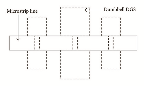
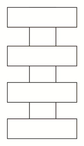
Periodic DGSs for planar microwave circuits are earning major attraction of microwave researchers. Microstrip lines with a periodic DGS have been presented: bandpass and low pass planar filters [37, 44, 45]. By using periodic structure phenomena higher slow wave rate with greater degree of miniaturization is achieved. Repetition of single defect with a finite spacing is referred to as periodic structure. By cascading the defects (resonant cells) in the ground plane the return loss level and bandwidth is improved depending on the number of periods. Shape of DGS unit, distance between two DGS units and the distribution of the different DGSs are the main parameters that affect the performance of periodic DGS. Two periodic DGS shapes are shown in Figure 2; horizontally periodic DGS (HPDGS) and vertically periodic DGS (VPDGS) are shown in Figures 2(a) and 2(b), respectively [29, 34].
Application, advantages, and disadvantages of different shapes of DGS are summarized in Table 2.
| S. number | Shape | Reference | Advantage | Disadvantage | Applications |
|---|---|---|---|---|---|
| 1 | Dumbbell | [12] | Simple structure, easy to design and analyse | Single stop band | Band-stop filter |
| 2 | HPDGS | [29] | 38.5% size reduction | Larger size than VPDGS, dispersion problem | Matching network of amplifier |
| 3 | VPDGS | [29] | 44.4% size reduction | Dispersion problem | Matching network of amplifier |
| 4 | U-slot | [14] | Improved Q-factor | Single stop band | Band-stop filter |
| 5 | V-slot | [14] | Improved Q-factor | Single stop band | Band-stop filter |
| 6 | Cross DGS | [15] | Sharp rejection, ultra-wide stop band | — | Low pass filter |
| 7 | Fractal DGS | [13] | Wide stop band | No sharp cut-off frequency | Band-stop filter |
| 8 | Spiral DGS | [30] | Multistop band | Complex analysis | Band-stop filter |
5. Equivalent Circuit Models of DGS
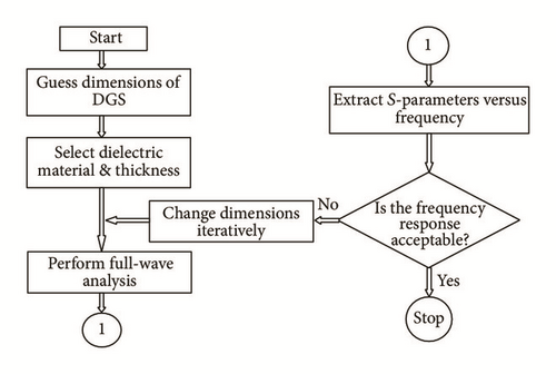
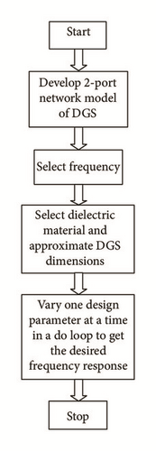
Each metallic part of microstrip antenna is a combination of distributed resistance, capacitance, and inductance. Hence each model may be represented by its equivalent circuit model. By Babinate’s principle each slot is reciprocal to its metallic structure and also may be represented by its equivalent resistance, capacitance and inductance model. Full-wave analysis is used for analysing the responses of DGS and to find the equivalent circuit model. However, Full-wave analysis fails to describe about the physical dimensions and position of the DGS. Conventional methods for analysing the DGS were based on trial and error iterative methods so they were time consuming and there was a possibility for not getting the optimum results [6, 31, 44, 103–106]. Figure 3 shows the conventional design and analysis methods of DGSs.
- (1)
LC and RLC equivalent circuits.
- (2)
π shaped equivalent circuit.
- (3)
Quasi-static equivalent circuit.
- (4)
Using ideal transformer.
| S. N | Method | Advantage | Disadvantage | Summary |
|---|---|---|---|---|
| 1 | LC and RLC [12] | DGS which have similar shape like dumbbell DGS have almost same characteristics like dumbbell DGS and could be analysed | Complex and cannot determine the location of DGS | An equivalent circuit model of one-pole Butterworth low pass filter |
| 2 | π shaped [31] | More accurate results in comparison with LC and RLC circuits | Complex and cannot determine the location of DGS | Explains both amplitude versus frequency and phase versus frequency characteristics |
| 3 | Quasi-static [32] | The limitations of full-wave analysis can be overcome by developing the equivalent circuit model depending upon quasi-static technique | Complex and cannot determine the location of DGS | Role of dimensions of the DGS is explained for creating the stop band characteristics |
| 4 | Using ideal transformer [33] | Can determine the location of DGS | — | A simple and accurate circuit model for the slotted ground plane with microstrip line |
5.1. LC and RLC Equivalent Circuits
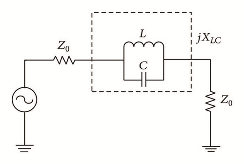
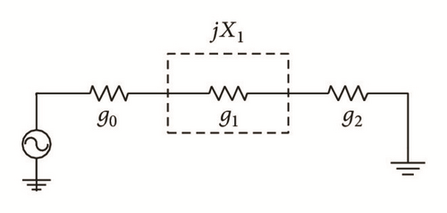
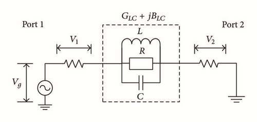
The LC equivalent circuit model of the DGS is shown in Figure 4. An equivalent circuit model of one-pole Butterworth low pass filter is shown in Figure 4(b). The current path is increased due to the rectangular parts of dumbbell DGS; thus effective inductance and effective capacitance of microstrip line are changed. The two rectangular slots of dumbbell DGS are responsible for adding a capacitive effect and a thin rectangular defected slot which connects both the rectangular shaped defects accounts for adding the inductance to the total impedance. Due to this LC circuit, a resonance is occurred at a certain frequency. The slotted area of the DGS is proportional to the effective inductance and inversely proportional to the effective capacitance. An increment in slotted DGS area gives rise to the effective inductance thus results in a lower cut-off frequency. A decrement in the DGS area reduces the effective capacitance, thereby increasing the resonant frequency.
5.2. π Shaped Equivalent Circuits
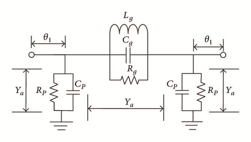
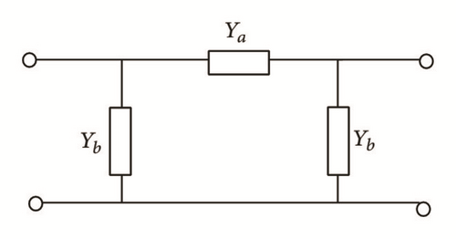
The π shaped equivalent circuit model shown in Figure 6 was proposed after LC and RLC equivalent circuit [31]. The π shaped equivalent circuit gives more accurate results in comparison with LC and RLC circuits.
5.3. Quasi-Static Equivalent Circuit
A quasi-static equivalent circuit model was presented by Karmakar et al. for a dumbbell shaped DGS [32]. Physical dimensions of dumbbell DGS play a vital role for determining the equivalent circuit model. This model is different from the two types of equivalent circuits mentioned above (LC or RLC model, and π shaped equivalent circuit) and depicted in Figure 7.
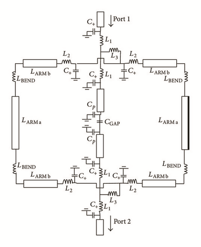
The limitations of full-wave analysis can be overcome by developing the equivalent circuit model depending upon quasi-static technique. Basic principle of DGS is included in this approach and the role of dimensions of the DGS is explained for creating the stopband characteristics. Optimization technique is used to evaluate the deferent structures of DGS because deferent shapes have different characteristics.
5.4. Using Ideal Transformer
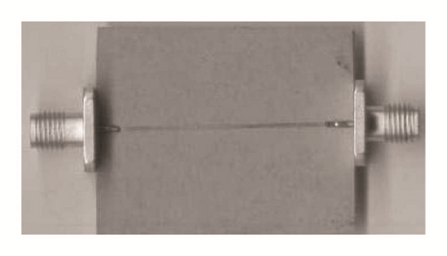
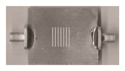
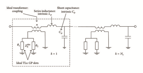
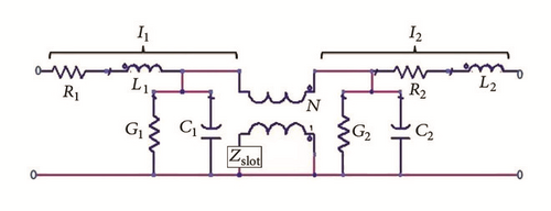
An equivalent circuit model for antenna also has been presented using ideal transformer [33]. A circular slot is embedded in the ground plane underneath an open ended microstrip line. Equivalent circuit model of the proposed DGS antenna is shown in Figure 10. Distributed parameters are used in the equivalent circuit.
6. Applications of DGS in Microwave Technologies
DGS is widely used nowadays in active and passive devices. Each DGS shape has its own characteristics and creates effect on the performance of the device according to its geometry and size. DGS has been used in filters, coplanar waveguides, microwave amplifiers, and antennas to improve their performance. DGS is used for miniaturizing the size of component, enhancing the operating bandwidth and gain, reducing the mutual coupling between two networks, suppressing the higher order harmonics and unwanted cross-polarization, and also producing notched band to stop interference with any band. Several applications of DGS available in literature are discussed further.
6.1. Filters
Numerous DGS shapes have been reported to design planar circuits. Different shapes of DGS have been explored to design bandpass and band-stop planar filters. Initially, a dumbbell shaped DGS was embedded in the ground plane underneath a microstrip line for creating a filter response. It perturbs the electromagnetic fields around the defect and trapped electric fields give rise to the capacitive effect, while the surface currents around a defect cause an inductive effect. This, in turn, results in resonant characteristics of a DGS, causing an effect of filters.
6.1.1. Low Pass Filter
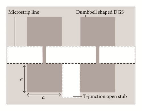
Single and cascaded dumbbell shaped DGSs were used with microstrip line and T-junction of microstrip line to design a low pass filter [12]. Two DGS units were integrated with a microstrip line as shown in Figure 11. The S-parameters shown in Figure 11(b) clearly explain their low pass response.
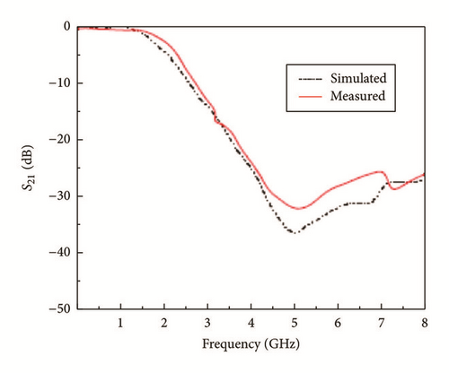
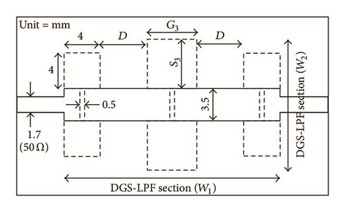
A new N-pole LPF design method using the DGS has been proposed [47] and depicted in Figure 12. The DGS-LPF neither has open stubs, nor high-impedance lines because a very wide microstrip line has been adopted to realize the shunt capacitors. An equivalent circuit also has been proposed to calculate the resonant frequency of LPF. The S-parameter response is shown in Figure 12(b).

Different shapes of DGS shown in Figure 13 have been presented by MK Mandal for LPF response [42]; circular dumbbell shaped DGS was presented with an equivalent circuit model. A quasi-static analysis approach has been reported for DGS filters by Karmakar et al. [32].
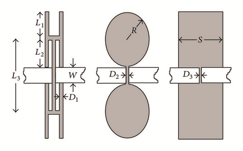
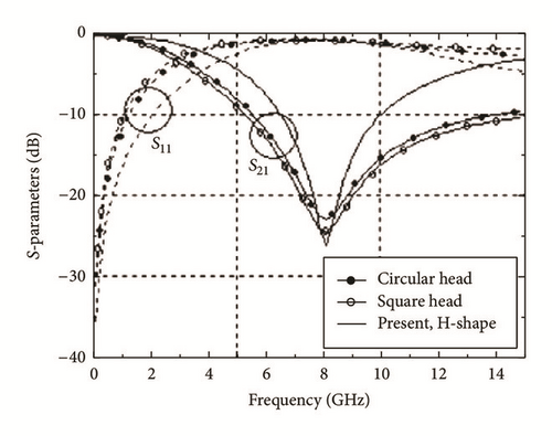
“I,” “H,” and “cross” shaped DGSs have been introduced with their equivalent circuit model for LPF [15]. An elliptical function response has been obtained using both dumbbell shaped and spiral shaped DGS under the single wide microstrip line [48]. A triangular dumbbell DGS has been used to synthesize microstrip DGS low pass filter [49]; π-equivalent circuit was presented to analyse the structure [49] as shown in Figure 14.
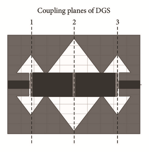
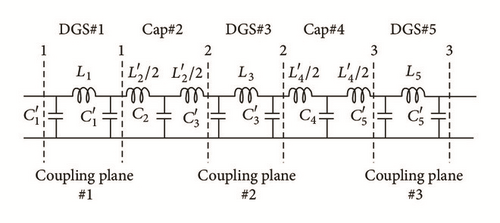
Complementary Square Ring Resonator (CSRR) has been used periodically to design the LPF [50]. Fractal dumbbell shaped DGS also has been reported for achieving the low pass filter response [51]. The circuit area of a LPF has been minimized with wide stop band characteristics [52].
6.1.2. Band-Stop Filter
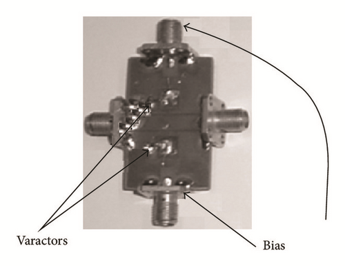
By embedding a defect on the metallic ground plane a certain band of frequency can be rejected and a planar band-stop filter can be realized. Surface wave and other leakage transmission are suppressed at this stopband. A square patch has been inserted inside the conventional dumbbell shaped DGS to modify its frequency response and to allow the control of the rejected frequency [17]. Low, high, or even multiple frequencies can now be rejected by the proper choice of the positions of the short circuits that can be placed along the circumference of the square patch. The varactor diode was used between the square patch and CPW ground to make it tuneable as shown in Figure 15.

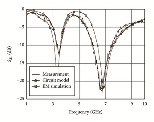
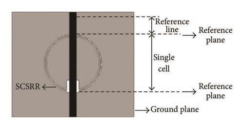
Semicomplimentary Split Ring Resonator (SCSRR) has been used for realizing the band-stop filter [53]. An equivalent circuit model was presented using an ideal transformer. Both single cell and double cell structures were proposed as shown in Figure 16.

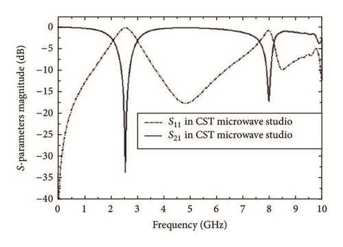

A wideband band-stop filter has been introduced using stepped impedance resonator and Defected Ground Structure [54]. A fabricated prototype of band-stop filter has approximately 139% 20-dB rejection bandwidth. Substrate Integrated Waveguide (SIW) also has been reported with DGS as a band-stop filter [55, 56]. The complex eigen value problems of the SIW cavity have been studied with an FDFD method and it has been shown that the SIW cavities can easily achieve high Q-factors [55]. It has been found that the proposed DGS SIW cavity filters present very promising performances with low insertion loss and high stopband rejection. Such types of filters are valuable in the design and realization of low cost microwave and millimeter-wave systems. Compactness has been achieved using a SIW filter with DGS resonators [56], with better frequency selectivity and wide stopband. In these designs, the DGS is etched on the ground plane of SIW cavity.
6.1.3. Bandpass Filter
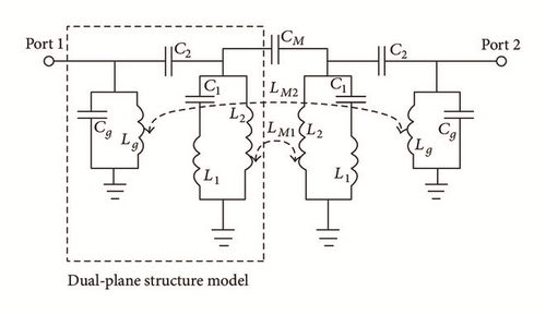
DGS also has been used for bandpass filter (BPF) response. Several researches have been reported for BPF with DGS. A wide stop band bandpass filter based on dual-plane interdigital DGS slot structure has been presented [57]. An equivalent circuit model also has been presented as shown in Figure 17. The filter has the merits of high selectivity and wide upper stopband.
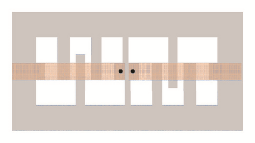
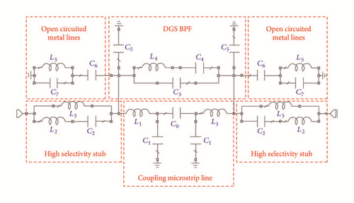
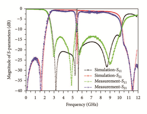
The bandpass filters with ultra-wideband (UWB) characteristics also have been proposed [58, 59]. A notch is implemented in UWB bandpass filter using open circuited line and DGS [58]; an equivalent circuit model also presented for analysing the structure theoretically. The schematics of open circuited line DGS BPF and its equivalent circuit model are shown in Figures 18 and 19, respectively.

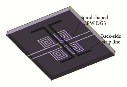
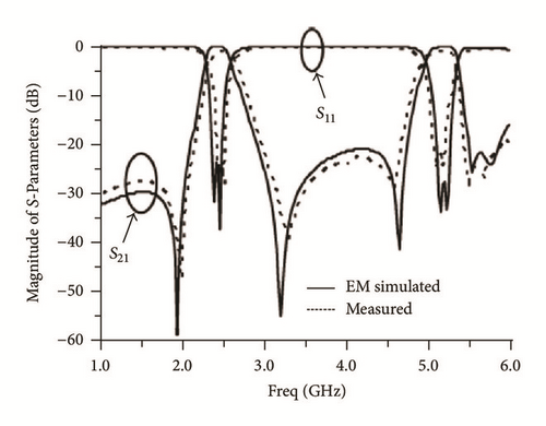
Dual-band bandpass filters also have been implemented using Defected Ground Structure [60–62]. Dual-band bandpass filter stacked with spiral shaped CPW Defected Ground Structure and back-side coupled strip lines have been proposed with quasi-elliptic function [60]. The filter shown in Figure 20, allows two transmission paths to RF signals, has a dual-band response and proposed for a WLAN application. The two quasi-elliptic function structures on different layers generate respective passband, and can change the operating frequency of each of them. Four poles in the stopbands are realized to improve the selectivity of the filter and the isolation between the two passbands. Dual-band BPF response has been achieved by using Defected Ground Structure waveguide [61]. A dual-band BPF with controllable second passband using a variable characteristic impedance transmission line in the stub loaded resonator has been reported [62]. The characteristic impedance of the transmission line can be controlled with the help of the Defected Ground Structure and the varactor diodes located in the ground plane. It was demonstrated that the second passband can be adjusted while keeping the first passband constant. The proposed filter provides low insertion losses throughout the entire tuning range of the second passband.
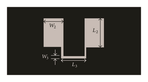
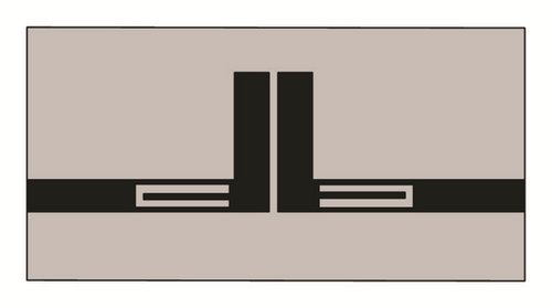
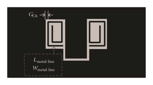
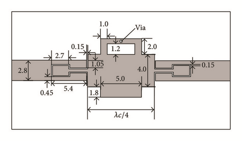
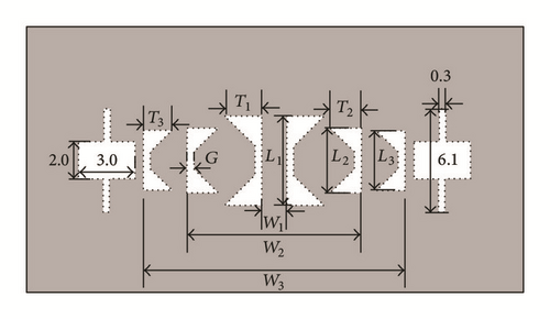
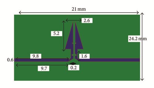
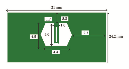
An ultra-wideband differential bandpass filter has been presented [63]. A narrow notched band is introduced and common-mode suppression is achieved using DGS. Using the slot-line DGS, the interference of notch structure is cancelled out for common-mode. Compared with former UWB differential filter structures, the proposed filter provides interference rejection function, wider bandwidth and simpler design theory and good common-mode performance, indicating potential applications in the UWB communication systems. Dual-notched compactness has been achieved using DGS in Ultra-Wideband Bandpass Filter [64]. The schematic diagram is shown in Figure 21. A compact Ultra-Wideband Bandpass Filter (UWB BPF) has been proposed using coupled lines incorporating arrow shape and U-slot Defected Ground Structures (DGSs) [65]. The input and output feeding lines are connected to the coupled lines on one side of the substrate while the U-slot DGS is etched in the other side of the substrate below the coupled lines as shown in Figure 22.
6.2. Coplanar Waveguide
Recently, a great trend towards the implementation of a reconfigurable DGS, where the location of the transmission zeros can be controlled and tuned, may be seen from a number of recent publications. In addition to this, DGS unit cell has been proposed on coplanar waveguide. Several studies have been reported in this regard [55, 56, 66–69]. Coplanar waveguides having band-stop performance have been proposed with DGS using SIW technique [55, 56]. Figure 23 shows the model of SIW embedded with DGS.
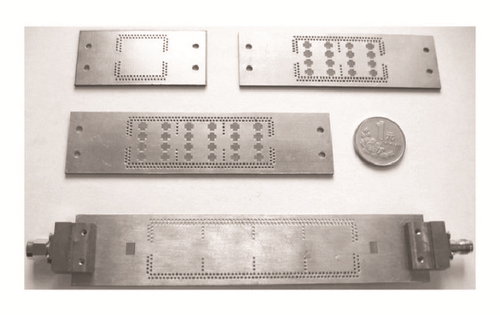
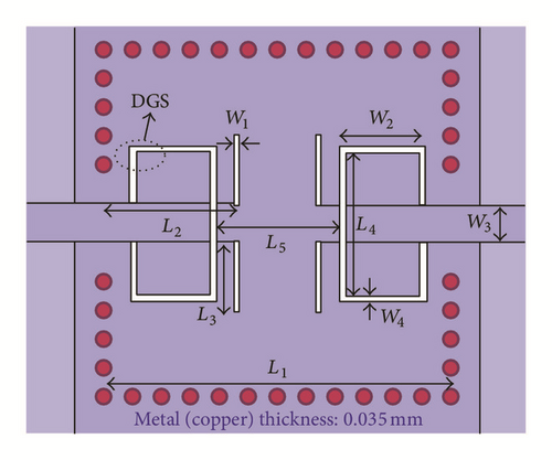
A reconfigurable DGS resonator on CPW has been proposed, which was capable of yielding arbitrary transmission zeros over the band 1–11 GHz [67]. Reconfigurability of the structure was achieved by using PIN diodes. Spiral DGS has been implemented on the top and bottom ground plane of the grounded CPW to produces the highest band-stop rejection and two independent band-stop resonances [68]. A compact reconfigurable band-stop resonator has been realized using DGS on CPW [69].
6.3. Amplifier
DGS also has been employed with planar microwave amplifiers. Lim et al. (2001) improved the efficiency of power amplifier using DGS [70]. As shown in Figure 24, a series of dumbbell DGS has been embedded on the ground plane underneath the microstrip line to improve the efficiency and to tune the harmonics of power amplifier.
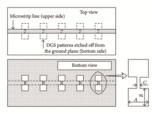
Further, Lim et al. (2002) proposed DGS to reduce the size of matching networks of microwave amplifiers using the slow wave characteristics of microstrip [71]. In order to reduce the size, while keeping the same electrical length, two and three DGS patterns were adopted in matching networks. DGS has been reported to suppress the harmonics of power amplifier with λ/4 bias line [21]. A DGS-based Doherty power amplifier has been proposed with suppressed harmonics [72].
6.4. Antenna
In the early phases of the development of DGS, a majority of DGS shapes were explored to design microstrip filters, and these applications inspired the antenna engineers to realize planar antenna with stopband characteristics by integrating DGS on their ground plane. DGS has been used for improving the various parameters of the conventional planar antenna. Different configurations have been explored since 1999 to achieve various goal as discussed below.
6.4.1. Circularly Polarized DGS Antenna
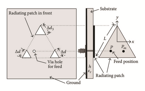
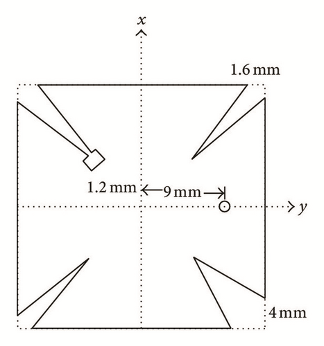
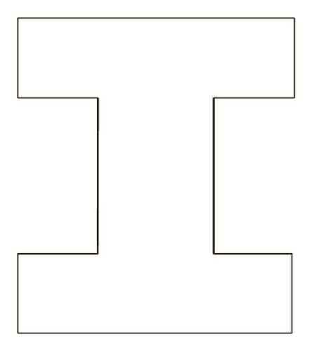
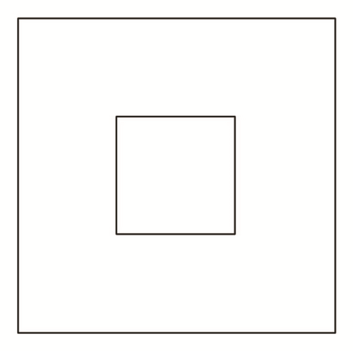
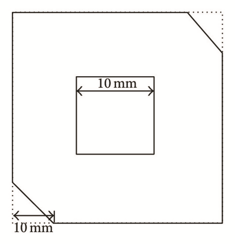
The latest communication devices should be compact, lightweight, inexpensive, and versatile and thus require circularly polarized microstrip antennas. Circular polarized microstrip antennas have been widely used for mobile communication, global positioning system (GPS), radio frequency identification (RFID) readers, and wireless local area network (WLAN) applications. They also provide a powerful modulation scheme in active read/write microwave tagging systems. DGS also has been integrated on the ground plane of the microstrip antennas for achieving the circular polarization (CP) [73–76]. Kuo and Hsieh achieved the CP using triangular shaped DGS coinciding with the corners of equilateral triangle [73], as shown in Figure 25. CP has been achieved in aperture coupled annular ring microstrip antenna using DGS [74]. A design approach for the circular polarization of the microstrip antenna has been implemented with the concept of unbalanced DGS feed lines [75]. A dual-band asymmetric slits loaded microstrip patch antenna has been proposed and CP was achieved using DGS in both bands of operation [76]. Deferent shapes of DGS used in [76] are shown in Figure 26.
6.4.2. Multiband Antenna
Multiband also can be achieved by using DGS. Several studies have been reported in this regard [76–83]. Dual broadband antenna with rectangular slot has been analysed for wireless applications [77]. A switchable single and multifrequency antenna depicted in Figure 27 is proposed with triple slot on the ground plane [78].
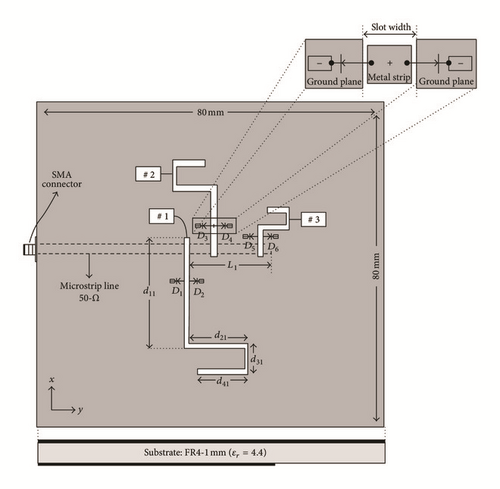
A microstrip-fed antenna design based on the patch monopole for a triple-frequency operation has been presented with DGS [79]. A triple band microstrip antenna has been realized and miniaturization was achieved using DGS [80]. A compact, DGS monopole antenna has been presented [81], which employs a single L-shaped slot in the ground plane of a conventional circular disc monopole antenna in order to achieve multiband performance. A low profile multifrequency-band printed antenna module has been presented. The radiator was a crescent-shaped microstrip patch with DGS [82]. A triple band microstrip patch antenna is proposed with DGS [83]; circular polarization is achieved by embedding the slots on ground.
6.4.3. Wideband Antenna
DGS also has been employed for wideband and ultra-wideband microstrip antennas. As shown in Figure 28(a), a square shaped defect has been integrated on the ground plane with an open ended microstrip line for enhancing the bandwidth of the microstrip antenna [84]. Further, a parasitic square element was used at the centre of the square defect on the ground plane underneath the open ended microstrip line as shown in the Figure 28(b) [85]. An impedance bandwidth of about 80% was achieved by using parasitic element at the centre of square DGS.

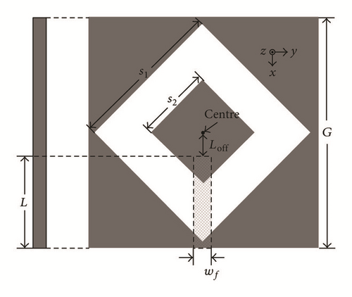
A double U-shaped DGS has been used to broaden the impedance bandwidth of a conventional microstrip-fed monopole antenna [86]. DGS has been integrated with probe fed rectangular microstrip patch antenna for improving polarization (co- to cross-polarized isolation) with enhanced bandwidth [87]. A pair of L-shaped slots and parasitic structures on the ground plane has been presented for enhancing the bandwidth of a square radiating patch [88].
6.4.4. Antenna with Notched Band
A simple and compact ultra-wideband microstrip-fed planar antenna with dual-band-stop characteristic has been presented [89]. A notch band of 600 MHz for band rejection of WLAN has been created by using a U-slot shaped DGS embedded underneath the microstrip line. A novel compact printed monopole antenna with dual-band-notched characteristics used for UWB applications has been presented and investigated [90]. Dual band-notched characteristic was achieved using a G-slot DGS in the ground of the feeding line and a pair of г-shaped stubs in the radiating patch. A printed monopole antenna with desired band-rejection characteristic, in the frequency band of DSRC systems and WLAN, has been proposed for UWB applications [91]. A compact UWB planar antenna with dual-notched bands has been presented and discussed [92]. The band notches were realized by I-shaped DGS as well as a L-shaped arm with shorting pin on the ground plane. For enhancing the impedance bandwidth novel techniques on the ground plane were used. A microstrip-fed printed monopole antenna with dual-band-notched characteristics has been proposed for UWB applications [93]. By using an arc-shaped stub on the back of the substrate, which was connected to the top patch through a cylindrical via pin, the lower notched band was achieved. To realize the wide notch band from 5.1 GHz to 5.9 GHz, a couple of stepped CLL elements were placed near the feeding line, and an arc-shaped slot was etched on the radiating patch. A log periodic dipole antenna has been proposed for UWB applications [94]. Half monopoles on the ground plane and half on the signal plane are placed for achieving the UWB response. And a U-shaped slot is introduced to achieve a notch band. A notch band is achieved at 4.6 GHz in an UWB antenna [95].
6.4.5. Size Reduction of Antenna with DGS
Effective capacitance and effective inductance of the model are changed by embedding the slots on the ground plane, resulting in shifting of resonance frequency to its lower side. Thus, compactness is achieved by using DGS. Several researches have been reported in this regard [33, 94, 95]. A compactness of 30% is achieved by using meandering slots in the ground plane [33]. A “T” shaped slot integrated in the ground plane to achieve the miniaturization and compactness of 80% has been achieved [96].
6.4.6. Cross-Polarization Suppression of Antenna with DGS
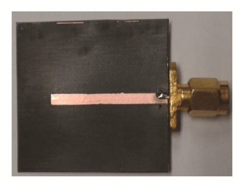
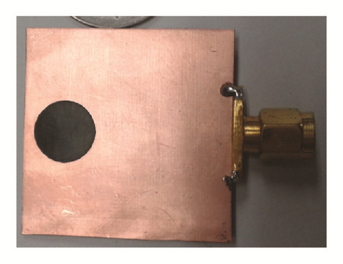
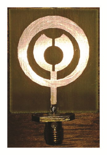
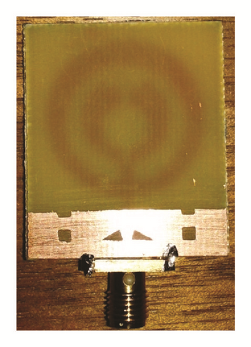
DGS has been reported for suppressing the cross-polarization level of the antenna. The cross-polarized radiation was theoretically studied in [97–100]. A suppression of 5 dB in cross-polarization level has been achieved by using dot shaped defects [25]. The suppression in cross-polarized radiations is improved to the value of 10–12 dB by using arc-shaped defects [98]. A 35 dB of isolation is achieved between copolar and cross-polarization level by using circular shaped DGS [97]. Fabricated prototypes of proposed antenna in [97] are shown in Figure 29. The cross-polarization level of the value of −36 dB is achieved in stacked microstrip antenna using DGS [99]. Minimum cross-polarization level of −42 dB is achieved by using DGS in UWB antenna shown in Figure 30 [100].
6.5. Negative Group Delay Circuits (NGDC)
A negative group delay circuit (NGDC) is used for time advancement for wave propagation and has been applied for various wireless applications. Chaudhary et al. have proposed miniaturization technique for NGDC using U-shaped DGS [101]. Attenuation characteristics of DGS and external resistor were used to achieve the desired amount of group delay at operating frequency. Two-stage NGDC was also designed and fabricated to enhance the group delay [101].
6.6. Variable Characteristics Impedance Line
DGS also has been used for designing the variable characteristics impedance line for power divider [102]. An unequal 1 : N Wilkinson power divider with variable power dividing ratio has been reported with DGS [102]. A fixed 1 : 6 divider with rectangular DGS and island was fabricated first; then unequal dividing ratio of divider was adjusted by varying the equivalent capacitance of varactor diode [102].
7. Conclusion
In this paper, the evolution of DGS is presented. The basic ideas behind the working principle are discussed. Circuit model and characteristics of deferent shapes of DGS are discussed. Deferent techniques are presented for analysing the DGS. The role of DGS in the field of microwave and microstrip antennas is presented with various applications of DGS, that is, miniaturization, multiband performance, bandwidth enhancement, gain enhancement, mutual coupling suppression between two elements, higher mode harmonics suppression, cross-polarization suppression, notched band creation, and circular polarization achievement. Applications of DGS in the field of Microwave Engineering are summarized in Table 4.
| S. N | Application | References |
|---|---|---|
| 1 | Low pass filter | [12, 15, 32, 42, 47–52] |
| 2 | Band-stop filter | [17, 53–56] |
| 3 | Band pass filter | [57–65] |
| 4 | Coplanar waveguide | [55, 56, 66–69] |
| 5 | Amplifier | [21, 70–72] |
| 6 | Circularly polarized antenna | [73–76] |
| 7 | Multiband antenna | [76–83] |
| 8 | Wideband antenna | [84–88] |
| 9 | Notched band | [89–95] |
| 10 | Size reduction | [33, 94–96] |
| 11 | Cross-polarization suppression | [25, 97–100] |
| 12 | Negative group delay circuit (NGDC) | [101] |
| 13 | Variable characteristics impedance line | [102] |
Competing Interests
The authors declare that they have no competing interests.


