Investigating the Effect of Thermal Annealing Process on the Photovoltaic Performance of the Graphene-Silicon Solar Cell
Abstract
Graphene-silicon (Gr-Si) Schottky solar cell has attracted much attention recently as promising candidate for low-cost photovoltaic application. For the fabrication of Gr-Si solar cell, the Gr film is usually transferred onto the Si substrate by wet transfer process. However, the impurities induced by this process at the graphene/silicon (Gr/Si) interface, such as H2O and O2, degrade the photovoltaic performance of the Gr-Si solar cell. We found that the thermal annealing process can effectively improve the photovoltaic performance of the Gr-Si solar cell by removing these impurities at the Gr/Si interface. More interestingly, the photovoltaic performance of the Gr-Si solar cell can be improved, furthermore, when exposed to air environment after the thermal annealing process. Through investigating the characteristics of the Gr-Si solar cell and the properties of the Gr film (carrier density and sheet resistance), we point out that this phenomenon is caused by the natural doping effect of the Gr film.
1. Introduction
The fascinating properties of graphene (Gr), such as high carrier mobility, high optical transparency, and tunable work function, make it an attractive candidate for application in optoelectronic and photovoltaic devices [1–4]. Recently, there is growing interest in incorporating Gr with silicon (Si) to develop graphene-silicon (Gr-Si) solar cell, in which the Gr film forms Schottky junction with Si functioning for carrier separation [5, 6]. To form Gr-Si Schottky junction, the Gr film can be simply placed onto a Si substrate at room temperature by the traditional wet transfer process [7] and the high temperature diffusion process needed for forming p-n junction is eliminated. Hence, the Gr-Si solar cell is considered as a potential low-cost alternative to the conversional crystallize silicon p-n junction solar cell. However, the impurities induced during the wet transfer process at the graphene/silicon (Gr/Si) interface, such as H2O and O2 (H2O/O2), may degrade the performance of the Gr-Si devices [8].
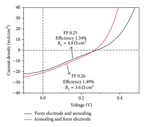
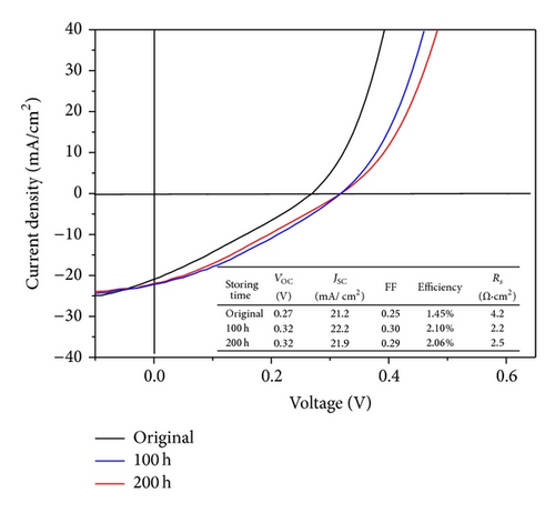
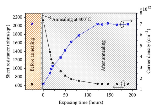
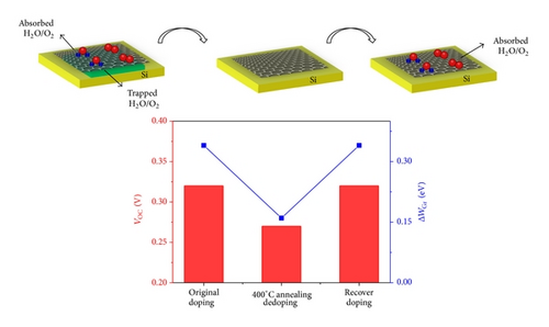
In this work, we demonstrate that the photovoltaic performance of the Gr-Si solar cell can be improved effectively by thermal annealing process. Particularly, the efficiency of the Gr-Si solar cell is enhanced by about ten times due to the reducing of the series resistance of the solar cell, which is believed to be resulting from the removing of the trapped H2O/O2 at the Gr/Si interface. More interestingly, when exposed to air ambient after the thermal annealing process, the efficiency of the Gr-Si solar cell is found to be improved furthermore. By systematically investigating the characteristics of the Gr-Si solar cell and the properties of the Gr film (carrier density and sheet resistance), we point out that the further performance enhancement for the Gr-Si solar cell is caused by the natural p-type doping of the Gr film due to the reabsorption of H2O/O2 molecules on the Gr film surface.
2. Experiments
2.1. Gr Preparation, Transfer, and Characterization
Monolayer Gr film was produced by a copper (Cu) catalyzed low pressure chemical vapor deposition (LPCVD) method at 1000°C, using CH4 (20 sccm) as the carbon source and H2 (40 sccm) as the reduction gas. Traditional PMMA-assisted wet transfer process was used for Gr film transfer. The PMMA dissolved in chlorobenzene was spin coated on Gr/Cu film at 4000 rpm for 30 s, followed by curing at 200°C for 10 min. After the Gr on the backside of the Cu foil was removed by exposing to ozone for 10 min, the Cu foil was etched away by a mixture of FeCl3 and HCl solution to get PMMA/Gr film. The PMMA/Gr film was rinsed in DI water for 3 times and then transferred onto the target substrate, and finally the PMMA was removed using acetone. The electrical properties of the Gr film (sheet resistance and carrier density) were measured with a Hall system (Lakeshore).
2.2. Gr-Si Solar Cell Fabrication and Performance Evaluation
N-type 〈100〉 Czochralski (CZ) Si wafer with resistivity of 1–3 Ω·cm was used as a substrate for the device fabrication. The Si wafer was cleaned by the IMEC clean process, and then it was exposed to ambient air for two hours before use. Subsequently, a monolayer Gr film was transferred onto the Si substrate with a traditional PMMA-assisted wet transfer process. Afterwards, the front contact was formed by applying Ag paste around the Gr film to enclose a nearly square window as the device-active area (~9 mm2) and the back contact was made by scratching the InGa eutectic alloy at the Si backside, thus forming a complete Gr-Si solar cell. After measuring the current density-voltage (J-V) characteristics of the resulting Gr-Si solar cell both in dark and under illumination, the Gr-Si solar cell was subjected to thermal annealing processes at given temperatures (200°C, 350°C, 400°C, and 450°C) for one hour under forming gas. After each thermal annealing process, the J-V curves of the Gr-Si solar cell were measured again and the InGa eutectic alloy at the backside of Si was removed completely before applying next thermal annealing process. The measurement system used here consists of a Keithley 2400 source meter and a solar simulator calibrated by a standard Si solar cell to provide a standard AM 1.5G illumination with intensity of 100 mW/cm2.
3. Results and Discussion
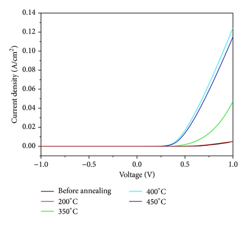
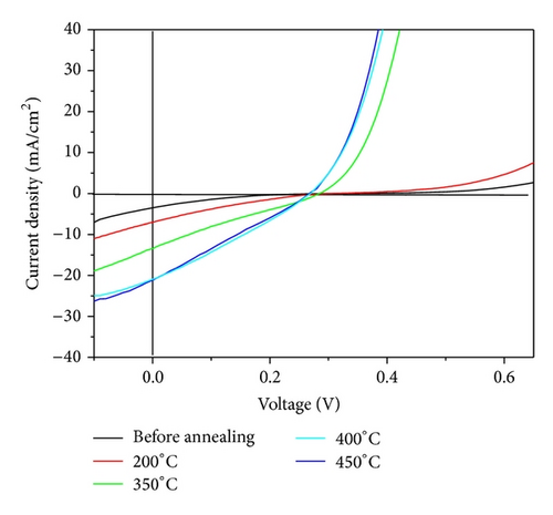
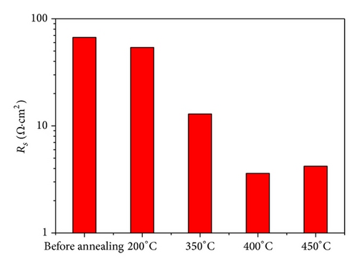
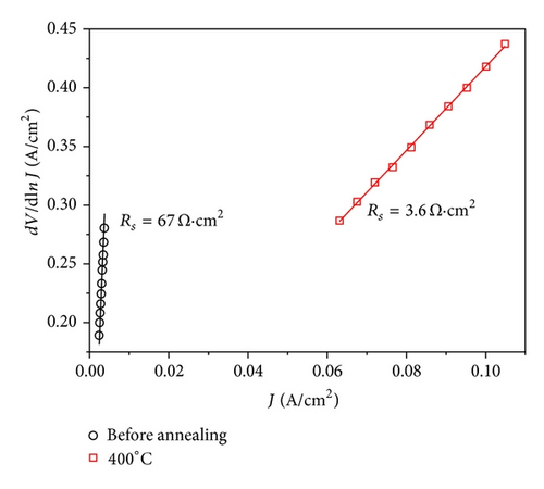
Figure 1 shows the J-V curves of the Gr-Si solar cell in dark and under illumination before annealing and after thermal annealing processes at different temperatures. It can be seen that the thermal annealing process improves the device characteristics both in dark and under illumination. In dark, the forward current of the Gr-Si diode increases progressively as the annealing temperature increases from 200°C to 450°C and the turn-on voltage of the Gr-Si diode slightly decreases. Under illumination, the photovoltaic performance of the solar cell is progressively enhanced as the annealing temperature varying from 200°C to 450°C. Particularly, the short circuit current density (JSC), the fill factor (FF), and the efficiency of the solar cell are increased from 3.5 mA/cm2 to 21.2 mA/cm2, from 0.13 to 0.25, and from 0.14% to 1.45%, respectively (see Table 1). It is also found that the efficiencies of the Gr-Si solar cell are nearly equal after thermal annealing process at 400°C and 450°C. Therefore, the optimal thermal annealing temperature for the Gr-Si solar cell is about 400°C. Similar measurements have been taken on three Gr-Si solar cell samples and the trends reported here reproduced on all the samples. Figure 2 shows the evolution of series resistance (Rs) of the Gr-Si solar cell with the thermal annealing temperature. It can be seen that the Rs of the Gr-Si solar cell is largely reduced as the annealing temperature varying from 200°C to 450°C. Particularly, the Rs of the solar cell decreases from ~70 Ω·cm2 before annealing to ~4 Ω·cm2 after thermal annealing at 400°C. This causes the increase of the JSC and FF of the solar cell as shown in Table 1.
| Annealing temperature | VOC (V) |
JSC (mA/cm2) |
FF | Eff. |
|---|---|---|---|---|
| Before annealing | 0.32 | 3.5 | 0.13 | 0.14% |
| 200°C | 0.31 | 7.0 | 0.18 | 0.39% |
| 350°C | 0.29 | 13.4 | 0.23 | 0.89% |
| 400°C | 0.27 | 20.9 | 0.26 | 1.49% |
| 450°C | 0.27 | 21.2 | 0.25 | 1.45% |
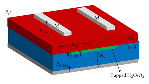
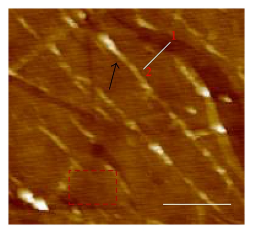
As shown in Figure 4, we suppose that the RC-GS is caused by the trapped H2O/O2 at the Gr/Si interface, which can block the transport of the carriers from the silicon to the Gr film and thus increase the Rs of the Gr-Si solar cell. The thermal annealing process can remove the trapped H2O/O2 at the Gr/Si interface and thus helps to reduce the Rs of the Gr-Si solar cell. Figure 5 shows the AFM images of the Gr film on Si substrate before and after thermal annealing at 400°C, respectively. It can be seen that the height of the Gr film before annealing is about 1.5 nm and the root-mean-square (rms) surface roughness of the Gr film is measured to be 0.54 nm. After thermal annealing at 400°C, these values decrease to 0.4 nm and 0.2 nm, respectively. This observation, according to our understanding, is due to the existence of trapped H2O/O2 at the Gr/Si interface, which can be removed by the thermal annealing process.



4. Conclusions
In summary, we found that the thermal annealing process can improve the photovoltaic performance of the Gr-Si solar cell effectively through removing the rapped H2O/O2 at the Gr/Si interface. The optimal annealing temperature is about 400°C. When exposed to the air environment after the annealing process, the photovoltaic performance of the Gr-Si solar cell can be improved furthermore thanks to the natural doping effect of the Gr film.
Conflict of Interests
The authors declare that there is no conflict of interests regarding the publication of this paper.
Acknowledgment
This work is supported by the National Natural Science Foundation of China (nos. 61422404 and 61274057).


