Nanoflake Manganese Oxide and Nickel-Manganese Oxide Synthesized by Electrodeposition for Electrochemical Capacitor
Abstract
Nanoflake structures of electrochemical manganese oxide (EMD) and nickel mixed manganese oxide (NiMD) were directly deposited on a stainless steel by using Chronoamperometry and Cyclic Voltammetry (CV) techniques. The structure, morphology, and capacitive behavior of EMD or NIMD nanoflake were affected by the electrodeposition modes and deposition time. The highest specific capacitance (Csp) was obtained for only two-minute deposition by both methods. EMD nanoflakes electrodeposited by CV technique show higher specific capacitance values than those prepared by Chronoamperometry owing to its homogenous and highly porous surface. All EMD samples exhibited excellent cycle behavior, less than 5% capacitance loss after 1000 cycles. Ni mixed MnO2 was prepared at different Mn2+/Ni2+ ratios for 2 minutes of electrodeposition. The presence of Ni2+ ion enhanced the Csp value at high charge-discharge rate due to the decrease of the charge transfer resistance. The supercapacitor prototype of 2 cm × 2 cm was assembled using EMD and NiMD as electrode material and tested at 1 A·g−1.
1. Introduction
Nanomaterials such as nanowires, nanorods, nanotubes, and nanoparticles have attracted great interest due to their unique physical properties (electrical, optical, and magnetic) and catalyst and chemical properties [1, 2]. Mostly used materials for supercapacitors include carbon materials, conducting polymers, and transitions metal oxides [1]. Manganese oxide shows excellent pseudocapacitive behavior with the large specific capacitance over 700 F/g in spite of the theoretical value of 1100 F/g [1, 3, 4]. Manganese oxide is a promising electrode material in supercapacitor due to its low cost, natural abundance, and being environmentally friendly compared to other pseudocapacitor materials [3]. In recent years, nanostructured manganese oxides have been thoroughly investigated for different potential applications such as catalysis for synthetic organic chemistry, water treatment, and energy storage devices [1–3]. Nanostructured manganese oxide was synthesized by chemical methods and physical methods. However, chemical methods have more benefits due to simplicity, economical effectiveness, and ability to control various structures and morphologies. Several methods have been suggested like chemical reduction, hydrothermal, sonochemistry electrochemical deposition, and sol-gel method [3]. The structural parameters such as crystal form, defect chemistry, morphology, porosity, and texture play a crucial role in determining and optimizing the electrochemical properties when using MnO2 as electrode materials (Table 1) [3].
| Technique | Morphology | Structure | SBET/m2·g−1 | Capacitance C, F/g |
|---|---|---|---|---|
| Hydrothermal [17] | Platelike, nanorod | α-MnO2 | 100–150 | 72–160 (200 mA·g−1) |
| High viscosity process [18] | Rod-shaped | α-MnO2, γ-MnO2 | — | 389 (10 mV·s−1) |
| Room temperature precipitation [19] | Rod-shaped | δ-MnO2 | — | 201 |
| Low temperature reduction [20] | Nanoflower | Cubic MnO2 (Fd3m) | 225.9 | 121.5 (1000 mA·g−1) |
| Sol-gel process [21] | Nanorods | γ-MnO2 | 317 (100 mA·g−1) |
One of the most common methods is electrochemical deposition due to its abilities to control the film thickness, structure, and morphology [5–9]. Pang et al. potentiostatically prepared the first electrodeposited thin film MnO2 electrode for electrochemical capacitor (ECs) in 2000 and their finding had sparked strong interest among energy research community for its application in supercapacitor electrode [5, 6]. Such high specific capacitance value arises from the ions insertion/desertion within MnO2 structure and it depends crucially on the particle size, surface, and porosity. Most of following studies have focused on varying the deposition parameters in order to achieve the enhanced electrochemical performance [7–13]. The MnO2 thin films can be prepared by anodic/cathodic electrodeposition. Cationic Mn2+ precursor is used in anodic oxidation while anionic (Mn7+) is used in cathodic reduction. In comparison, cathodic reduction offers more versatility as various metals could be codeposited during the deposition process. Oxidation of the metallic substrate during anodic deposition could also be avoided [14–16].
In this work, MnO2 (EMD) and Ni mixed MnO2 (NiMD) were electrochemically synthesized by Cyclic Voltammetry (CV) and Chronoamperometry (CA) and characterized for supercapacitor application. For Ni mixed MnO2, the Ni content of binary oxide was investigated to find out the optimized capacitive value, high power density, and electrochemical stability. Material characterization was carried out by Transmission Electron Microscopy (TEM), Raman spectroscopy, Infrared Spectroscopy, Cyclic Voltammetry (CV), and charge-discharge cycling. Excellent capacitor values and stability of binary oxide Ni-MnO2 were demonstrated.
2. Experimental
2.1. Synthesis Process
All chemical reagents are analytical grades: MnSO4·H2O (99%, Sigma Aldrich), Na2SO4 (99%, Prolabo Chemical), and Ni(NO3)2·6H2O (Sigma Aldrich). For MnO2 electrochemical deposition, aqueous solutions of 0.3 M MnSO4 and 0.05 M Na2SO4 (solution A) were prepared in distilled water just before use. The pH of solution A is neutral (pH ~ 7).
Stainless steel (SS) sheet of grade 214 with 2 cm × 2 cm surface and thickness of 0.5 mm was used as substrate for electrodeposition. The EMD and NiMD samples were performed by using Biologic-MPG 2 potentio/galvanostat system at room temperature in three-electrode cell. The electrochemical cell includes a stainless steel as working electrode (WE), a titanium mesh as auxiliary electrode (AE), and a saturated Ag/AgCl (in 3 M KCl) electrode as reference electrode (RE).
EMD and NiMD materials were synthesized by Chronoamperometry (CA) and Cyclic Voltammetry (CV) method. By using CA method, MnO2 thin film was deposited in galvanostatic mode at 1.2 V versus Ag/AgCl on SS substrate. In CV method, MnO2 thin film was formed during potential sweep in range of 0-1 V versus Ag/AgCl (sat) at scan rate of 50 mV/s. The deposition time of EMD samples was investigated from 2 to 12 minutes for each method (Table 2).
| Time (minutes) | CV method | CA method |
|---|---|---|
| 2 | EMD-CV2 | EMD-C2 |
| 4 | EMD-CV4 | EMD-C4 |
| 6 | EMD-CV6 | EMD-C6 |
| 8 | EMD-CV8 | EMD-C8 |
| 10 | EMD-CV10 | EMD-C10 |
2.2. Characterization
The structure of electrodeposited samples was characterized by using Raman spectroscopy and Fourier Transform Infrared Spectrometer (FTIR) IFS 28 Brucker. The IR absorption was carried out over the wavelength range 400–4000 cm−1. The surface morphology and particle size were determined using a Scanning Electron Microscopy (SEM) JSM 6480 LV and Transmission Electron Microscopy (TEM) JEOL JEM 1400. Stylus Profilometer was carried out by Dektak 6 M equipment in order to determine thickness of MnO2 films. The contact angle of thin film was measured using Data Physics Optical Contact Angle OCA20 in order to check the wetting property in aqueous solution.
The specific capacitance (Csp) of supercapacitor was also evaluated by Galvanostatic charge-discharge method. The 2 × 2 cm supercapacitor prototypes, containing electrodeposited material on SS substrates used as current collector, were used for cycling test and were charged-discharged at current density of 1 A·g−1.
3. Results and Discussion
3.1. FTIR and Raman Characterization
The structure of thin films EMD and NiMD was characterized by using IR and Raman spectroscopy. Figure 1 showed the spectra of EMD deposited in 2 minutes by two methods in 400–4000 cm−1. The samples were abbreviated as EMD-CV2 and EMD-C2.
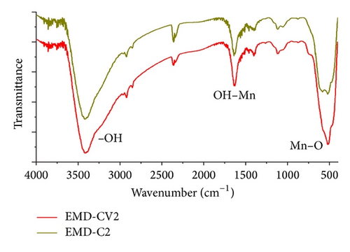
The vibration at 3400 cm−1 indicated –OH vibration mode of the water. As thin film was prepared in the aqueous solution, a tunnel structure MnO2 can be formed during the electrodeposited process. Thus, H2O molecules can be intercalated in the tunnel of thin film [8]. The vibration bands at 1600 cm−1 and 500 cm−1 were assigned to Mn–O stretching modes of MnO6 octahedral sites. These vibration modes are similar to those of natural mineral nsutite samples (γ-MnO2 structure, complex tunnel), but some features are not clearly determined [8].
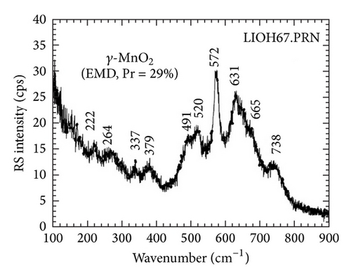
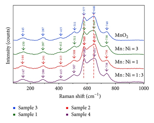
An examination of Raman spectroscopy is presented in Figure 2 for EMD and NiMD thin films with various Mn : Ni ratios. Compared to the study of Julien et al. [22], the vibration mode of MnO2 thin film at 577 cm−1 (ν3), 640 cm−1 (ν2), and 740 cm−1 (ν1) corresponds to the stretching modes of the MnO6 octahedral. The corresponding antisymmetry stretching modes are recorded in the infrared spectrum at 517 cm−1 and 621 cm−1 (Figure 2). The weak Raman bands at 511, 415, 297, and 145 cm−1 are assigned to the deformation modes of the metal-oxygen chain of Mn–O–Mn in the MnO2 octahedral lattice. The Ni mixed MnO2 (NiMD) sample exhibited similarly Raman vibration bands. However, the shifted modes were clearly observed, for example, the blue shift for (ν2) and (ν3) vibration and the red shift for (ν1) vibration. Also, the vibration peaks at lower wavenumber were shifted (Figure 2). The results showed that the presence of Ni ion affected the local structure of MnO2, typically the short range environment of oxygen coordination around transition metal cations in MnO2 lattice.
3.2. Morphology and Wettability Studies
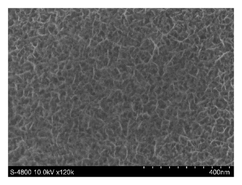
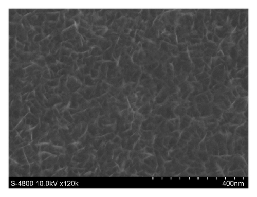
Figures 3 and 4 show SEM images of EMD and NiMD thin films. The surface porosity and nanoflakes dimension were also affected by deposit time and the deposition mode. A slight difference was observed when the electrodeposition mode changed (Figures 3(a) and 3(c)). Generally, the surface morphology of thin films is composed entirely of nanoscale fiber (nanoflakes). An irregular interconnection of nanofibers formed a highly porous network. By using CV method, the nanofiber slightly grows up. The nanoflakes dimension is about 100–120 nm in length compared to 40–60 nm of which prepared by CA method. As the deposition time is long, the nanofibers grow up quickly and the interconnection points seem to be a star form (Figures 3(c) and 3(d) for 12 minutes electrodeposition). Due to the variation of surface porosity and nanofiber morphology, the specific capacitance behavior is expectedly changed [1].
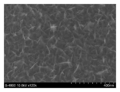

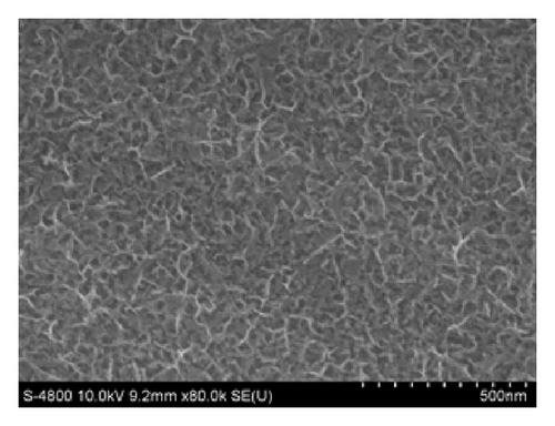
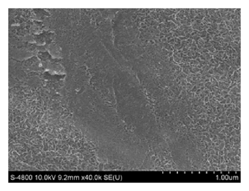
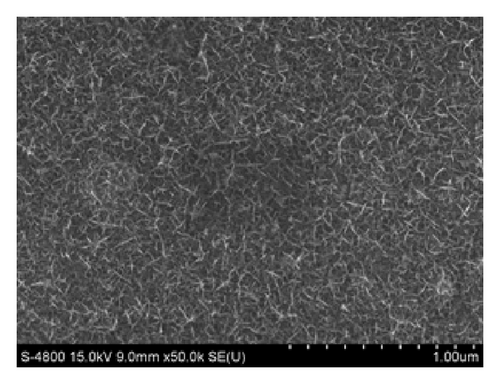
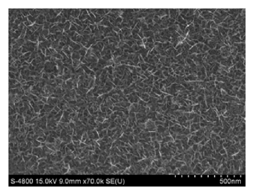
In case of Ni mixed MnO2, the surface morphologies seem to be similar to those of MnO2 films (Figure 4). Using CV method exhibits homogenous surface covered of well-formed nanoflakes.
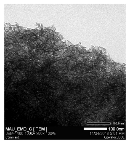
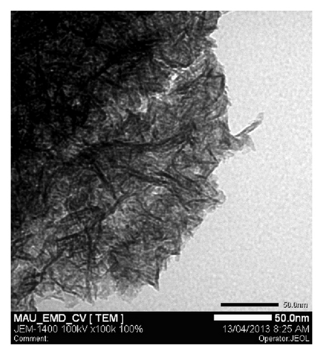
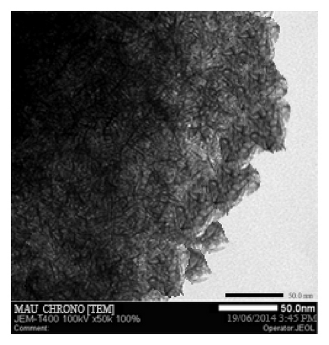
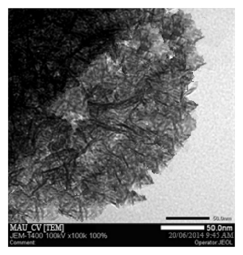
TEM images were performed for Ni mixed MnO2 (NiMD) at the same electrodeposition conditions (Figure 5). In general, it was observed that film structure prepared in two minutes is dense. The nanoflakes seem to be very fine and tend to interweave to make a network.
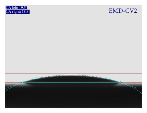
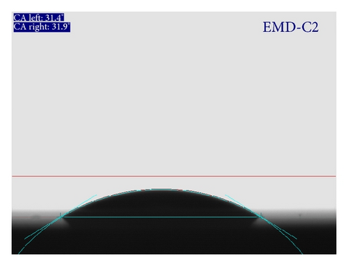
Wettability test is carried out in order to investigate the interaction between liquid and thin film surface. As the wettability is high, the small contact angle (θ) resulted and the surface is hydrophilic. In contrast, the surface is hydrophobic. Both hydrophilic and hydrophobic properties can be applied to many fields from medicine to engineering, especially in energy storages [1]. Figure 6 shows the contact angle measured for MnO2 films prepared by CA and CV method. Both films are expectedly hydrophilic due to the presence of –OH group on the surface and in the structure. Indeed, the results in Figure 6 indicated that contact angle is less than 90°. In addition, EMD-CV2 thin film is more hydrophilic than EMD-C2. The hydrophilicity is essential for electrochemical reaction on the electrode/aqueous electrolyte interface.
3.3. Electrochemical Properties of Electrodeposited Thin Film
The capacitance behavior of MnO2 and NiMD thin films was tested using CV in potential range of 0-1 V at 100 mV/s. Figure 7 shows CV curves of MnO2 thin films prepared by CA and CV method in 1 M Na2SO4.
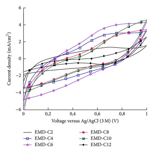
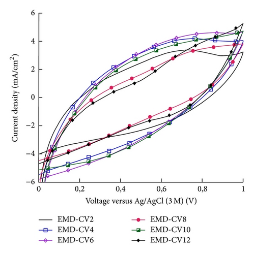
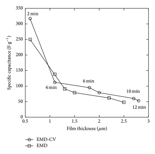
The specific capacitance (Csp) was calculated by using (1). EMD was prepared by CA method; EMD-CA exhibited the Csp values that are 250, 138, 91, 79, 62, and 48 F/g for EMD-C2, EMD-C4, EMD-C6, EMD-C8, EMD-C10, and EMD-C12, respectively. With CV method, the Csp values are 317, 112, 95, 79, 60, and 53 F/g for EMD-CV2, EMD-CV4, EMD-CV6, EMD-CV8, EMD-CV10, and EMD-CV12, respectively. Previous studies [2, 3, 6] show that capacitances of manganese oxide synthesized by electrochemical deposition were about 200–300 F/g.
The highest Csp was obtained at two minutes of electrodeposition for both methods (Figure 7(c)). The thickness of MnO2 film is about 0.55 μm. Thus, it can be concluded that the thin and porous film was only obtained in a short deposition time. When the deposition time is long, the nanoflakes grew up fast and their interconnection makes the film more compact than a short-time deposition. Thus, penetration of electrolyte into the film as well as the specific capacitance decreases due to the increase of electric resistance. The small thickness of MnO2 film is necessarily required in order to obtain the good electric conductivity and specific capacitance [4, 12].
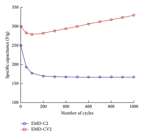
The electrochemical stability of thin films was evaluated. Figure 8 shows the specific capacitance (Csp) of EMD-C2 and EMD-CV2 measured at a scan rate of 100 mV/s. Among EMD-C samples, the highest initial capacitance was obtained for EMD-C2. The Csp value keeps constant, about 170 F/g after 200 cycles. For EMD-CV2, the Csp decreases slightly after 100 cycles before increasing significantly to 330 F/g in the following cycles. After 1000 cycles, the fading of Csp of EMD-C2 and EMD-CV2 was 23% and 5%, respectively (see Figure 10). Thus, the nanostructured EMD-CV2 seems to be better for supercapacitor application than EMD-C2. In fact, this fade observed for EMD samples can be explained by the structure evolution in aqueous solution, so the metal ion doping into MnO2 lattice would improve the structural stability.
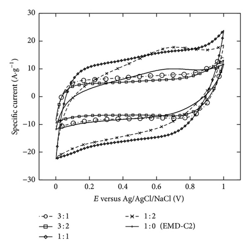
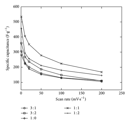
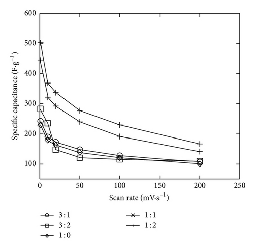
The two minutes electrodeposition was chosen to study the Ni mixed MnO2 (NiMD) at different Mn2+ : Ni2+ ratios. Figures 9(a) and 9(b) show the CV electrochemical properties of NiMD samples prepared by two deposition methods. In comparison to the EMD samples, the NiMD exhibited the same shape type of voltammogram but larger magnitude current. It can be observed that the CVs are more rectangular and symmetrical but lower in current magnitude at high Mn2+/Ni2+ ratio than at the low ratio. Thus, the characteristics indicate the ideal capacitive behavior with high reversibility of NiMD sample. The highest Csp was obtained for NiMD samples at Mn2+/Ni2+ = 1 : 1 at all scan rates (Figures 9(c) and 9(d)).

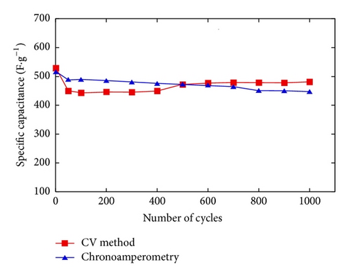
The electrochemical stability of NiMD thin films prepared at Mn2+/Ni2+ = 1 : 1 was also evaluated (Figure 11). In comparison to the EMD at the same deposition condition, NiMD samples exhibited higher Csp, about 500 F/g versus 300 F/g. By changing the electrodeposition modes, the NiMD-CV shows the Csp increase after 500 cycles, from 430 F/g to 500 F/g while NiMD-CA keeps constant during 800 cycles; after that a slight fading is observed at the final cycles. After 1000 cycles at 100 mV/s, the fading of Csp is less than 7% for NiMD samples. The fact that Ni ion doping into MnO2 lattice increases Csp as well as electrochemical stability was briefly reported by Rajendra Prasad and Miura [23]. In this work, the highest Csp was obtained about 480 F/g at 100 mV/s for NiMD sample (65% wt MnO2 : 35% wt NiO).
3.4. Electrochemical Properties of Supercapacitor Prototype
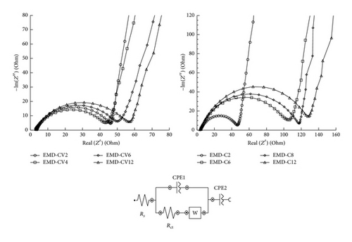
Electrochemical impedance spectroscopy (EIS) measurements were also carried out in the frequency range of 100 kHz–0.1 Hz. Figure 11 shows the Nyquist plots of EMD thin films prepared at various deposition times by two methods.
The Nyquist plot shows a high-frequency intercept on the real axis corresponding to the electrolyte resistance (RΩ); a semicircle is considered as a parallel combination of charge transfer resistance (Rct) and double-layer capacitance (Cdl) with a linear region at low-frequency range. In the low-frequency region, linear part of the plot exhibits an angle between 45 and 90°.
The EIS data was analyzed by the electrical equivalent circuit which consists of (RΩ) the electrolyte resistance, (Rct) charge transfer resistance, constant phase element (CPE) used instead of double-layer capacitance (Cdl), Warburg (W) arising from a diffusion controlled process at low-frequency, and CPE assigned to pseudocapacitance of the material in the low-frequency because of nonideal capacitive behavior. The starting nonzero intercept at Z′ at beginning of semicircle is identical in all the curves and its electrical resistance of Na2SO4 around 1 Ω. For CA method, the charge transfer values of EMD-C2, EMD-C6, EMD-C8, and EMD-C12 are 43 Ω, 102 Ω, 116 Ω, and 126 Ω, respectively. For CV method, the charge transfer values of EMD-CV2, EMD-CV4, EMD-CV8, and EMD-CV12 are 40 Ω, 42 Ω, 47 Ω, and 55 Ω, respectively. It means that the increase of deposition time (or film thickness) decreases the charge transfer resistance. Thus, a high resistance caused a difficult charge transfer electron between interface electrolyte and interface electrode.
At the same deposition conditions, the charge transfer resistance of NiMD samples decreases significantly compared to EMD (Figure 12).
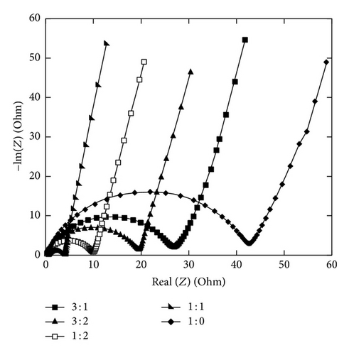
As the Mn2+/Ni2+ increase, the semicircle diameter becomes smaller. The lowest resistance was obtained for NiIMD at Mn2+/Ni2+ = 1 : 1, about 4 Ω versus 10 Ω at Mn2+/Ni2+ = 1 : 2 (Figure 13).
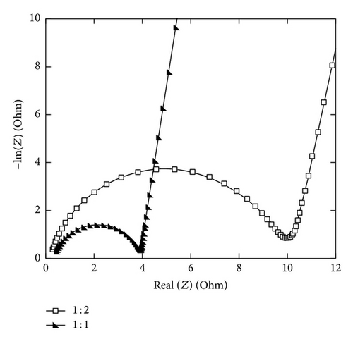
The Ni ion addition to the MnO2 lattice would improve the electrical resistivity of MnO2 film in addition to enhance the specific capacitance. It maybe also enhanced the power density as well as reversibility of the supercapacitior at high charge-discharge rate. Symmetrical capacitor prototypes of 2 cm × 2 cm were assembled with two thin films of electrodes EMD-CV2 and NiMD-CV at Mn2+/Ni2+ = 1 : 1 and characterized by charge-discharge cycling at very high current 1 A·g−1.
Figure 14 shows charge-discharge values of EMD and NIMD sample at current 1 A·g−1. The efficiency of charge-discharge cycling is about 0.9. Discharge Csp values were calculated by using the current density, discharge time, and the weight of material. Csp values obtained from Figure 14 for EMD-CV2 and NiMD-CV are 10 F·g−1 and 25 F·g−1. As expected, supercapacitor of NiMD-CV based electrode exhibits a higher power density than EMD-CV2.
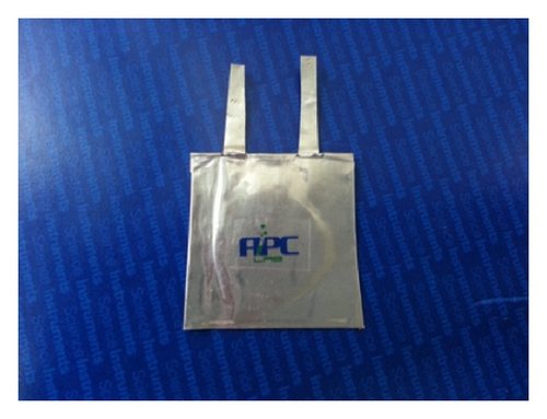
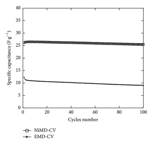
The stability of supercapacitor based on NiMD-CV and EMD-CV2 was also tested for a large number of cycles (up to 10,000 cycles) at 2 A·g−1. A Csp fading of 25% and 14% was observed with NiMD-CV or EMD-CV2 based capacitors, respectively, after 10,000 charge-discharge cycles. There is an initial large Csp decrease and then the Csp remained almost constant. The NiMD-CV exhibited expectedly higher stability than EMD-CV2 based capacitor. Thus, it would be promising for the long-term capacitor application.
4. Conclusions
Nanoflakes EMD and NiMD with high porosity were prepared by two electrochemical depositions modes. The thin films exhibited the γ-MnO2 based structure. The Ni addition to MnO2 lattice affected the local structure of γ-MnO2 that was evidently observed by using Raman spectroscopy. The EMD-CV exhibited better electrochemical behavior (Csp and charge-discharge stability) than EMD-C due to the homogenous film forming and high porosity during the reduction-oxidation sweep. With short-time deposition (2 minutes), EMD thin films show the highest Csp and lowest charge transfer resistance. Compared to EMD electrodes prepared at the same deposition, NiMD films enhance significantly the Csp values as well as electrochemical stability. The highest Csp value was 500 F·g−1 compared to 300 F·g−1 of EMD. The enhanced electrectrochemical performance of NiMD can be explained by the increase of thin film conductivity with the presence of ion Ni2+. Moreover, high power density and excellent stability of assembled supercapacitor based on NiMD electrode materials were demonstrated (Csp of 25 F·g−1 at 1 A·g−1, 14% capacitance fade for 10,000 cycles).
Conflict of Interests
The authors declare that there is no conflict of interests regarding the publication of this paper.
Acknowledgments
The authors acknowledge funding from VNU-HCM under Grant HS2013-76-01. The authors would like to thank Office of Naval Research Global (ONRG) for Grant N62909-13-1-N235. The authors would like to thank the technical support of Horiba’s Representative Company in Vietnam.


