Novel Receiver Architecture for LTE-A Downlink Physical Control Format Indicator Channel with Diversity
Abstract
Physical control format indicator channel (PCFICH) carries the control information about the number of orthogonal frequency division multiplexing (OFDM) symbols used for transmission of control information in long term evolution-advanced (LTE-A) downlink system. In this paper, two novel low complexity receiver architectures are proposed to implement the maximum likelihood- (ML-) based algorithm which decodes the CFI value in field programmable gate array (FPGA) at user equipment (UE). The performance of the proposed architectures is analyzed in terms of the timing cycles, operational resource requirement, and resource complexity. In LTE-A, base station and UE have multiple antenna ports to provide transmit and receive diversities. The proposed architectures are implemented in Virtex-6 xc6vlx240tff1156-1 FPGA device for various antenna configurations at base station and UE. When multiple antenna ports are used at base station, transmit diversity is obtained by applying the concept of space frequency block code (SFBC). It is shown that the proposed architectures use minimum number of operational units in FPGA compared to the traditional direct method of implementation.
1. Introduction
The goal of third generation partnership project (3GPP) long term evolution-advanced (LTE-A) wireless standard is to increase the capacity and speed of wireless data communication. The LTE-A physical layer is a highly efficient means of conveying both data and control information between an enhanced base station, popularly known as eNodeB, and mobile user equipment (UE). It supports both frequency division duplex (FDD) and time division duplex (TDD) configurations in uplink and downlink operations. Further, it provides a wide range of system bandwidths in order to operate in a large number of different spectrum allocations [1].
LTE-A standard has six physical channels for downlink. They are physical broadcast channel (PBCH), physical downlink shared channel (PDSCH), physical multicast channel (PMCH), physical downlink control channel (PDCCH), physical hybrid automatic repeat request (ARQ) indicator channel (PHICH), and physical control format indicator channel (PCFICH). PBCH carries the basic system information for the other channels to be configured and operated in the LTE-A grid. The PDSCH is the main data-bearing channel. PMCH is defined for future use. In LTE-A, the control signals are transmitted at the start of each subframe in the LTE-A grid. PDCCH is used to carry the scheduling information of different types such as downlink resource scheduling and uplink power control instructions. PHICH is used to send the acknowledgement/negative acknowledgement bit to UEs to indicate whether the uplink user data is correctly received or not. PCFICH carries the control information about the number of orthogonal frequency division multiplexing (OFDM) symbols used for transmission of downlink control information. The high data rate in LTE-A requires high processing demands on all layers of the system which includes high digital signal processing (DSP) hardware processing in the physical layer. Further, the hardware implementation of receiver structures of various physical channels in LTE-A becomes a challenging task as the computational complexity increases.
In [2], receivers were designed for a 2 × 2 antenna system and for quadrature phase shift keying (QPSK) modulation and quadrature amplitude modulation (16-QAM and 64-QAM). Though successive interference cancellation (SIC) receiver meets the timing requirements in the LTE system, it is complex and the K-best list sphere detector (K-LSD) receiver has high latency. In [3], field programmable gate array (FPGA) and application specific integrated circuit (ASIC) implementations of receivers based on the linear minimum mean-square error (LMMSE), the K-LSD, iterative successive interference cancellation (SIC) detector, and the iterative K-LSD algorithms are carried out for spatial multiplexing based LTE-A system. The SIC algorithm is found to perform worse than the K-LSD when the MIMO channels are highly correlated, while the performance difference diminishes when the correlation decreases. The ASIC receivers are designed to meet the decoding throughput requirements in LTE and the K-LSD is found to be the most complex receiver although it gives the best reliable data transmission throughput. It is shown that the receiver architecture which could be reconfigured to use a simple or a more complex detector as the channel conditions change would achieve the best performance while consuming the least amount of power in the receiver. FPGA implementation of MIMO detector based on two typical sphere decoding algorithms, namely, the Viterbo-Boutros (VB) algorithm and the Schnorr-Euchner (SE) algorithm, is carried out in [4]. In this implementation method, three levels of parallelism are explored to improve the decoding rate: the concurrent execution of the channel matrix preprocessing on an embedded processor and the decoding functions on customized hardware modules, the parallel decoding of real/imaginary parts for complex constellation, and the concurrent execution of multiple steps during the closest lattice point search. The implementation of low-complexity codebook searching engine is proposed to support both LTE and LTE-A operations [5]. In [6], VLSI implementation of a low-complexity multiple input multiple output (MIMO) symbol detector based on a novel MIMO detection algorithm called modified fixed-complexity soft-output (MFCSO) detection is presented. It includes a microcode-controlled channel preprocessing unit, separate channel memory, and a pipelined detection unit. MATLAB-based downlink physical-layer simulator for LTE only for research applications is presented [7]. In [8], maximum likelihood- (ML-) based receiver structures are developed for decoding the downlink control channels PCFICH and PHICH in LTE wireless standard and the performance of the receivers has been analyzed for various configurations. The analytical results were validated against computer simulations but hardware implementation of the structures was not coded or synthesized. In [9], direct implementation of receive algorithms was carried out in FPGA for downlink control channels in LTE. However, most of these works either propose architectures for FPGA implementation or analyze the performance of various receiver structures in a generalized manner. The objective of this paper is to propose novel architectures for FPGA implementation of transmit and receive processing of downlink PCFICH channel in LTE-A standard in particular.
1.1. Transmit and Receive Processing of PCFICH
In PCFICH, the control format indicator (CFI) contains a 32-bit code word that represents the value of CFI as 1, 2, 3, or 4. The CFI informs the UE about the number of OFDM symbols used for the transmission of PDCCH information in a subframe. The 32-bit code word corresponding to the value of CFI is scrambled and QPSK modulated. The resultant 16 QPSK complex symbols are mapped to the resource elements of the first OFDM symbol of every subframe after layer mapping and precoding to obtain transmit diversity when two or more antenna ports are used at eNodeB [10]. The 32-bit code words for the four possible values of CFI are given in Table 1. A general block diagram of the transmitter and receiver processing of PCFICH is shown in Figure 1.
| CFI | 〈b31, …, b0〉 |
|---|---|
| 1 | 01101101101101101101101101101101 |
| 2 | 10110110110110110110110110110110 |
| 3 | 11011011011011011011011011011011 |
| 4 | 00000000000000000000000000000000 |
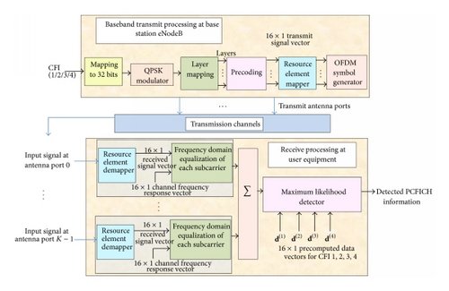
The OFDM signal is transmitted through a frequency selective fading channel. It is assumed that the number of receive antenna ports at UE is K. At each receive antenna port of the UE resource-element demapping follows the cyclic prefix removal and fast fourier transformation (FFT). The 16 × 1 receive signal vector at each antenna port is equalized in frequency domain at each subcarrier using the corresponding 16 × 1 channel frequency response vector. The outputs of frequency domain equalizer from each antenna port are summed up. The resultant 16 × 1 complex vector is applied to the maximum likelihood (ML) detector for detecting the CFI value. The objective of this paper is to synthesize and implement the receiver architecture for PCFICH.
The paper is structured as follows. Section 2 explains the system model and basic implementation architectures for single input single output (SISO) and single input multiple output (SIMO) configurations. The system model and basic implementation architecture for multiple input single output (MISO) and multiple input multiple output (MIMO) configurations are described in Sections 3 and 4, respectively. The proposed implementation architectures using folding and superscalar methods are given in Section 5 for SISO, SIMO, MISO, and MIMO configurations. Section 6 analyzes the performance of the proposed architectures and Section 7 concludes the paper with remarks on future work.
2. System Model and Implementation Architecture for SISO and SIMO Configurations
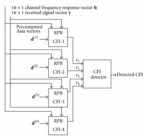
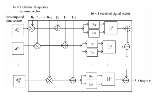
Figure 2 shows the basic architecture for estimating CFI using (2), in SISO configuration. The received signal vector y and the channel frequency response vector h are provided as input to the four receiver processing blocks (RPB) along with precomputed data vectors d(1), d(2), d(3), and d(4). The internal diagram for RPB CFI-1 is shown in Figure 3. It computes the expression assuming the CFI = 1. In RPB-m, the precomputed data vector d(m) is multiplied element by element with the channel frequency response vector. The resultant (16 × 1) vector is subtracted from the (16 × 1) received signal vector y. The sum of squared magnitude of each element in the resultant vector is the output of RPB.
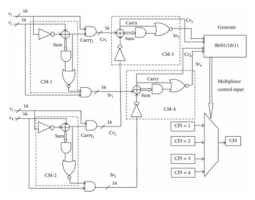
The multiplexer control input is activated based on the outputs from CM-3 and CM-4. One of the four outputs Cr3, Sr3, Cr4, and Sr4 would be “1” based on the minimum value of four inputs r1, r2, r3, and r4, respectively. Based on this 00, 01, 10, or 11 in the multiplexer control unit would be activated to obtain the detected CFI value.
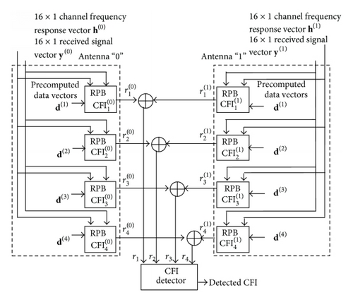
The basic architecture for estimating CFI using (6) in 1 × 2 SIMO configuration shown in Figure 5 is similar to the basic architecture of SISO configuration. The received signal vector y(k) and the channel frequency response vector h(k) are provided as input to the four receiver processing blocks (RPB-) at kth receive antenna, along with precomputed data vectors d(1), d(2), d(3), and d(4). The outputs from the mth RPB at 0th receive antenna and 1st receive antenna are added to get the mth input rm of the CFI detector circuit.
3. System Model and Implementation Architecture for MISO Configuration
In MISO and MIMO configurations, space frequency block code (SFBC) based layer mapping and precoding are carried out to obtain transmit diversity when two or more antenna ports are used at eNodeB as per the 3GPP LTE wireless standard [1, 11]. It is assumed that 2 antenna ports are used at eNodeB. The 16 × 1 complex symbol vector output of the modulation mapper is applied to the layer mapper. The 8 × 1 symbol vectors at layer 0 and layer 1 are given by [d0, d2, d4, d6,d8, d10, d12, and d14] and [d1, d3, d5, d7,d9, d11, d13, and d15]. The precoding is carried out using the SFBC in the LTE-A standard. The precoder output at antenna port 0 (A0) and antenna port 1 (A1) is shown in Figure 6.

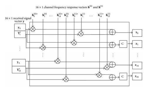
The PCFICH receive architecture for 2 × 1 MISO configuration is shown in Figure 7. Receiver decoding block (RDB) gets the 16 × 1 received signal vector y and computes the decoder output vector using (10), assuming that the channel frequency response vectors h(0) and h(1) are known. The detailed internal architecture of RDBM is shown in Figure 11. The decoder output vectors zi, i = 0, 2, 4, … , 14 are stacked as 16 × 1 vector . The 16 × 1 precomputed data vectors for CFI = 1,2,3,4 are represented as s1, s2, s3, and s4 respectively.
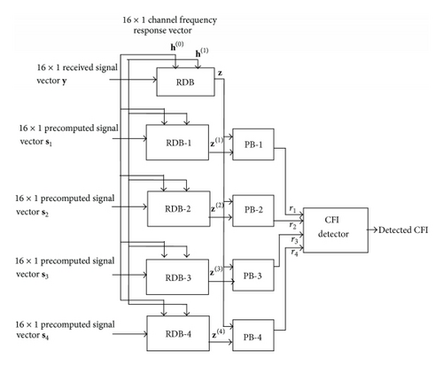
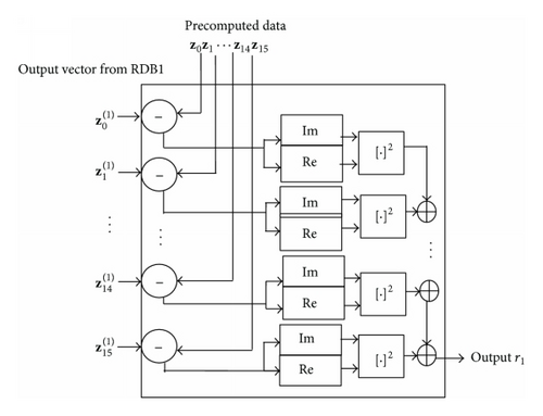
The detailed structure of receiver decoding blocks (RDB) is shown in Figure 8. The output vectors z(1), z(2), z(3), z(4) from RDB-1 to RDB-4 are fed to the processing blocks (PB-1 to PB-4). The detailed architecture of PB-1 is shown in Figure 9. The sum of the square magnitude of the elements of difference vector between decoded output vector z and the precomputed data vector s1 is the output r1 of PB-1. Similarly r2, r3, and r4 are computed for CFI = 2, 3, and 4 using PB-2, PB-3, and PB-4, respectively. The processing block outputs r1, r2, r3, and r4 are applied to the CFI determination circuit shown in Figure 4 to detect the CFI value.
4. System Model and Implementation Architecture for MIMO Configuration
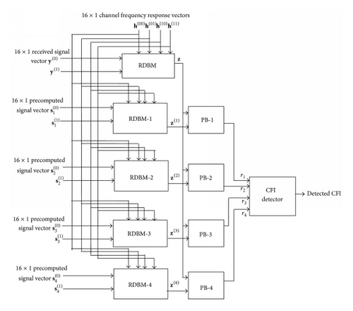
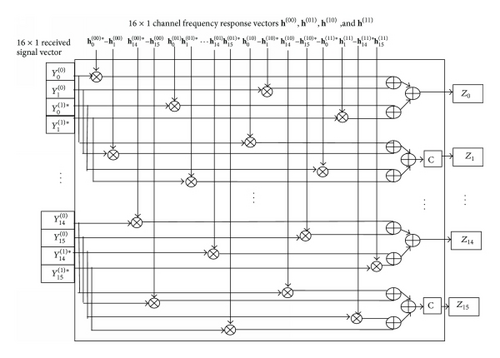
Receiver decoding block (RDBM) gets the 16 × 1 received signal vector y and computes the decoder output vector using (14), assuming that the channel frequency response vectors h(00), h(01), h(10), and h(11) are known. The 16 × 1 precomputed data vectors for CFI = 1, 2, 3, and 4 are represented as , , , and , respectively, for antenna 0, and as , , , and , respectively, for antenna 1. The received signal vectors and multiply with the four channel estimation vectors to give decoded output vector z that is sent to the processing block (PB) which is shown in Figure 9. The decoder outputs zi, i = 0, 2, 4, …, 14 are stacked as 16 × 1 vector . Similarly, RDBM1 gives output vector z(1) using the precomputed data vectors and and channel estimation vectors. The architecture of PBs and the CFI detection architecture are similar to that of the MISO system. The sum of the squared magnitude of the difference between each element in the decoded output vector z and its precomputed data in the vector z(1) is the output r1 of PB1. Similarly r2, r3, and r4 are computed for other CFI. The r1, r2, r3, and r4 are compared to determine the minimum value by the CFI detector shown in Figure 4.
5. PCFICH Receiver Implementation Methods
The PCFICH receiver architectures can be implemented directly based on the basic architectures developed in Sections 3 and 4. But, in order to effectively utilize the resources in FPGA, the implementation of basic architectures is done using the modified novel architectures based on VLSI DSP techniques, namely, folding and superscalar processing approach.
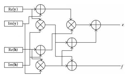
5.1. Direct Implementation with Multiplicands Rearranged Method
5.2. Proposed Architecture Using Folding Method
Folding architecture systematically determines the control circuits in DSP architectures where multiple algorithmic operations are time-multiplexed to a single functional unit [12]. It is used for synthesis of DSP architectures that can be operated at single or multiple clocks. It reduces the number of hardware functional units (FUs) by a factor of N at the expense of increased computation time.
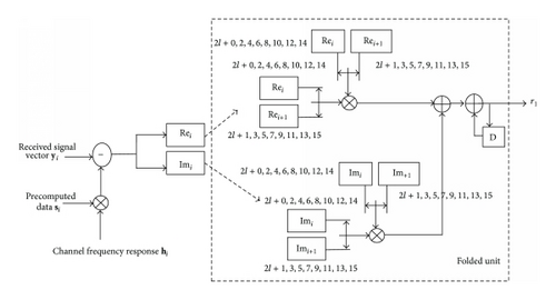
The folding architecture is introduced in the receiver structure of RPB in SISO and SIMO configurations and of RPB and PB in MISO and MIMO configurations as shown in Figures 13 and 14, respectively. For SISO RPB, there are 16 hardware lines to calculate the value of r1 each requiring two multipliers. Hence the number of multipliers used in one RPB is 32. In order to reduce the number of multipliers and adders, folding architecture is proposed. This architecture uses only two multipliers and performs the operation of a single hardware line 16 times in sequential way. The difference between the product of channel frequency response vector with the precomputed data vector and the received signal vector is stored in registers. At a time, one resultant signal pair involves in computation using two multipliers to get the value of zi. Four switches operating in system clock speed are involved in the architecture where two switches are used to pass the real part of the signal to one multiplier, while the other two switches are used to pass the imaginary part of the signal to another multiplier. The multipliers pass the products to the first adder for zi. The output of the first adder is passed to the second adder with a delay to accumulate the values z0 to z15 into a register in subsequent clock cycles. This process requires 16 clock cycles and the CFI is detected at the 17th clock cycle. Though it takes longer time for the clock cycles to get the output, the resources are minimized in this method.
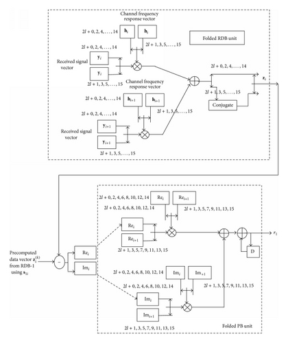
The folded architecture of decoding block of MISO and MIMO involving complex multiplication of the channel frequency response vector and the receive signal vector is shown in Figure 14. There are 2 complex multiplications and one addition in each of the 16 hardware lines. Hence total resource elements used are 32 complex multiplications and 16 additions. The folded architecture which reduces to just 2 complex multiplications and one addition requires five switches. Two switches are used to pass the first element of the receive signal vector and its corresponding channel frequency response vector to one multiplier and other two switches are used to pass the second element of receive signal vector and its channel frequency response vector to another multiplier. These four switches operate in system clock speed. The multipliers pass their products to the adder through the fifth switch before moving to PB. This process requires 16 clock cycles and the CFI is detected at the 17th clock cycle.
5.3. Proposed Architecture Using Superscalar Method
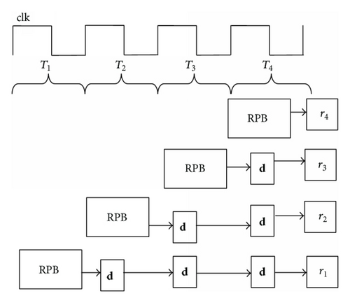
Superscalar approach is another low resource utilizing VLSI DSP technique. The superscalar processing method includes parallel processing and pipelining strategies. In this case, parallel operation for the 16 pairs of hardware lines is arranged with pipelining of the subtraction and square magnitude operations for each CFI. SISO configuration does not have complex multiplications and it has only square magnitude operations. Hence the RPB of SISO has 16 hardware lines each having 2 multipliers which results to a total of 32 multipliers. This setup requires more hardware resources than folding, but the output is obtained at every 4th clock cycle as shown in Figure 15. SIMO configuration which involves two receive antenna signal processing, requires twice the number of multiplications as that of SISO and the output is obtained at every 4th clock cycle. The block “d” represents the delay element introduced to buffer the values and produce the outputs at the same time instant.
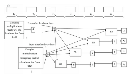
For MISO configuration the RDB has 16 hardware lines, with 2 complex multiplications each. Since each complex multiplication requires four real multiplications, RDB can be executed in two clock cycles by reusing 64 multipliers. 32 multipliers are required for PB taking 4 clock cycles. Hence 96 multipliers are required in MISO configuration. For MIMO configuration, the RDB requires reuse of 128 multipliers taking 2 clock cycles and an additional 32 multipliers are required for the PB taking 4 clock cycles. Hence 160 multipliers are required for MISO configuration and the output is obtained at every 6th clock cycle as shown in the Figure 16. The block “d” represents the delay element introduced to buffer the values and produce the outputs at the same time instant.
6. Results and Discussion
The proposed receiver architectures for PCFICH in SISO, SIMO, MISO, and MIMO configurations are implemented using the Xilinx PlanAhead tool on the Virtex-6 FPGA xc6vlx240tff1156-1 device board. The target device Virtex-6 has only 768 DSP elements. Table 2 shows the performance of the proposed architectures using folding and superscalar methods being compared with the direct implementation of PCFICH receiver, in terms of resource utilisation, speed, and power for all the SISO, SIMO, MISO, and MIMO configurations. The proposed architectures based on folding and superscalar processing methods require less number of resource elements.
| Diversity | Method | Multipliers | Adders | DSP elements |
LUTs | Total delay (ns) |
Speed (MHz) |
Dynamic power |
|---|---|---|---|---|---|---|---|---|
| SISO | Direct | 125 | 245 | 125 | 5479 | 39.081 | 25.587 | — |
| Folding (16T) | 8 | 81 | 16 | 2561 | 114.448 | 8.737 | 84 | |
| Superscalar (4T) | 32 | 182 | 66 | 2731 | 69.333 | 14.423 | 93 | |
| SIMO | Direct | 250 | 494 | 250 | 10942 | 40.278 | 24.827 | — |
| Folding (16T) | 16 | 165 | 32 | 5117 | 130.704 | 7.651 | 159 | |
| Superscalar (4T) | 64 | 318 | 130 | 5623 | 53.873 | 18.562 | 170 | |
| MISO | Direct | 224 | 580 | 594 | 14880 | 43.023 | 23.243 | — |
| Folding (16T) | 14 | 101 | 39 | 3950 | 255.264 | 3.917 | 173 | |
| Superscalar (6T) | 96 | 338 | 196 | 6156 | 80.495 | 12.423 | 208 | |
| MIMO | Direct | 320 | 844 | 675 | 17380 | 56.962 | 17.555 | — |
| Folding (16T) | 20 | 155 | 46 | 4395 | 256.528 | 3.898 | 374 | |
| Superscalar (6T) | 160 | 465 | 262 | 6932 | 85.822 | 11.652 | 382 | |
In the folding approach, resource utilization is less compared to the direct and superscalar approach at the cost of reduced speed of operation but it is suitable for real-time frame timings. When the LTE-A system operates at 1.4 MHz bandwidth, maximum time available for detection at each subcarrier is 992.063 ns since each slot of 0.5 ms duration in a frame (10 ms radio frame duration) consists of 7 OFDM symbols and there are 72 subcarriers along one OFDM symbol. The total delay in the receiver architecture is within the LTE time constraint. The dynamic power consumption is less in the folding method compared to superscalar method due to decrease in block arithmetic. Direct method does not require sequential execution and clocking and hence total power consumption is due to static power. Hence, it is inferred that the proposed architecture based on folding method is more suitable for CFI detection. The simulation waveform of the proposed architecture based on folding method is shown in Figure 17 for SISO, SIMO, MISO, and MIMO configurations.
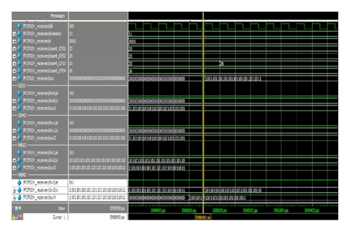
A general architecture based on folding method which operates at all the four SISO, SIMO, MISO, and MIMO configurations has also been developed. In this architecture, a control variable “e” is used to enable or disable the submodules SISO, SIMO, MISO, or MIMO according to the selection input “diversity.” CFI is detected at every 17th clock cycle. The synthesis results of a general architecture based on folding show that it utilizes minimum resources in XC6VLX240TFF1156-1 Virtex 6 device (768 DSPs). This is summarized in Table 3. Dynamic power consumption is due to internal switching contributed by the clock (246 mW), logic (670 mW), and the block arithmetic (103 mW).
| Parameter | Multipliers | Adders | Minimum clock period (ns) | Total delay (ns) | Speed (MHz) |
Total dynamic power (mW) |
|---|---|---|---|---|---|---|
| Value | 58 | 518 | 16.033 | 256.528 | 3.898 | 1019 |
Figure 18 shows the RTL schematic of 4 diversity blocks “div0,” “div1,” “div2,” and “div3” corresponding to SISO, SIMO, MISO, and MIMO controlled by wires named “e.” Power consumed includes both static power and dynamic power due to internal switching.
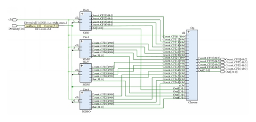
Figure 19 shows the resource utilization graph which shows the percentage of registers, lookup tables (LUTs), slices, DSP elements, and buffers used.
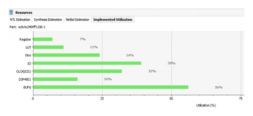
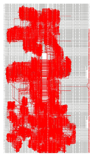
Figure 20 shows the implemented device in FPGA editor with the implemented components and interconnections between the components configured into the FPGA device.
7. Conclusion
In this paper, low complexity, low resource single, or multiantenna CFI detection at the receiver system has been proposed and analyzed using modelsim and implementation in the Virtex-6 device in Xilinx PlanAhead tool. In the receiver, computational complexity and the resource utilization are minimized by employing arithmetic operational rearrangement and suboptimal sequential DSP algorithm called the folding approach. The proposed architecture using folding method complies with the LTE frame timing constraint in SISO, SIMO, MISO and MIMO configurations. It is a suitable solution for the area optimized hardware implementation of receiver structures for PCFICH. In future, a total hardware accommodating all the physical downlink control channels of the 3GPP-LTE-A with low resource utilization could be synthesized and implemented.
Conflict of Interests
The authors do not have direct financial relation with any commercial identity mentioned in the paper or any other conflict of interests.
Acknowledgments
The authors wish to express their sincere thanks to All India Council for Technical Education, New Delhi, for the Grant to do the Project titled Design of Testbed for the Development of Optimized Architectures of MIMO Signal Processing (no. 8023/RID/RPS/039/11/12). They are also thankful to the Managements of Mepco Schlenk Engineering College, Sivakasi, and Thiagarajar College of Engineering, Madurai, for their constant support and encouragement to carry out this research work successfully.


