Optimization of Fractional-N-PLL Frequency Synthesizer for Power Effective Design
Abstract
We are going to design and simulate low power fractional-N phase-locked loop (FNPLL) frequency synthesizer for industrial application, which is based on VLSI. The design of FNPLL has been optimized using different VLSI techniques to acquire significant performance in terms of speed with relatively less power consumption. One of the major contributions in optimization is contributed by the loop filter as it limits the switching time between cycles. Sigma-delta modulator attenuates the noise generated by the loop filter. This paper presents the implementation details and simulation results of all the blocks of optimized design.
1. Introduction
In this equation, M is an integer, and n is the fractional part. To obtain the desired fractional division ratio dual modulus is used [7]. Using the sigma-delta modulation technique, we can remove the fractional spurs. This technique generates a random integer number. The average of these random numbers will result in the desired ratio. A phase detector, a loop filter, and a voltage controlled oscillator (VCO) are the main parts of phase-locked loop, as shown in Figure 1.
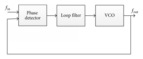
The important part of the phase-locked loop (PLL) is phase detector. It is also called a phase comparator, logic circuit, frequency mixer, or an analog multiplier that generates a voltage signal and this voltage signal shows the phase difference. Three units are coupled as a feedback system as shown in Figure 1. The periodic output signal is generated by the oscillator. The applications of PLL are versatile; for example, it can generate different stable frequencies or it can obtain a signal from noisy signals. A complete phase-locked loop block can be obtained from single integrated circuit. This technique is used in advanced electronic products which have different output frequencies from some Hz to many Giga Hz [8]. To get low power consumption, high speed, and stability, we decide to design phase-locked loop of architecture fractional-n using 0.12 micrometer CMOS/VLSI design. As the demand of PLL is growing day by day in the field of communications, low leakage transistors will be used for maintaining low power but for this we have to make a little compromise on frequency.
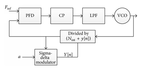
The structure of FNPLL is depicted in Figure 2. We can control characteristics of PLL by using low pass filter, for example, transients response and bandwidth. The basic and essential functional unit of PLL is VCO. VCO is used for clock generation [9]. For synthesizing aspired frequencies, we use PLL with arbitrary frequency division (+N) method. This proposed technique has the ability to give fast settling time, reduce phase noise, and also reduce the effect of spurious frequencies when compared with existing FNPLL techniques.
2. PLL Design Using 0.12 Micrometer
2.1. Phase Detector
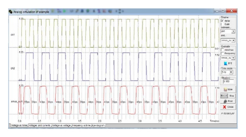
The first block has two inputs, the reference input and the feedback. It compares frequencies of input and produces an output using phase difference of inputs. To represent this block XOR gates are used. The gate produces a square wave when one-fourth of period shift of 90 degrees takes place at clock input, whereas output is different for all other angles. We apply output of the XOR gates to LPF which results in analog voltage, proportional to phase difference.
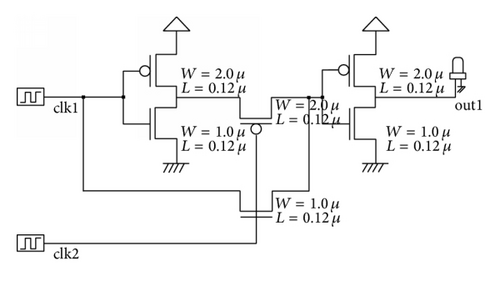
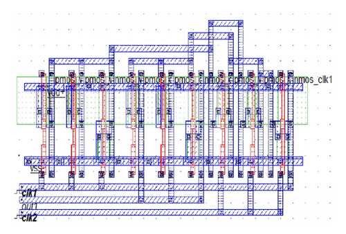
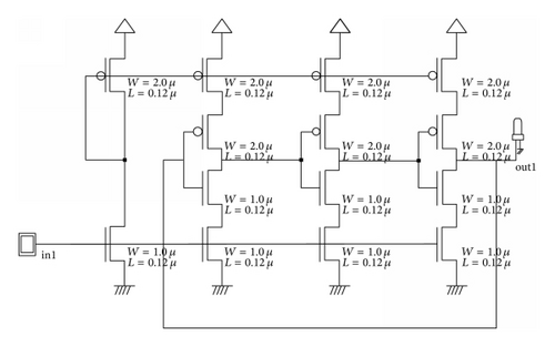
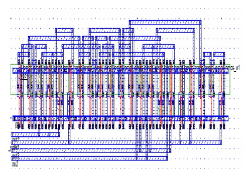
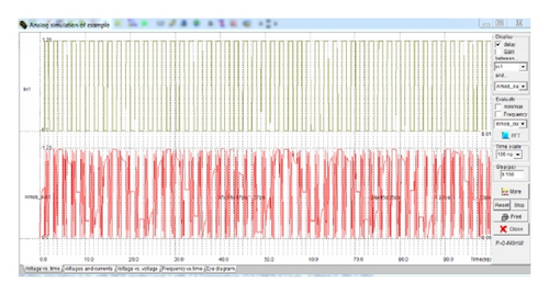
Figure 3 depicts a CMOS circuit of phase detector, Figure 4 describes layout, and Figure 5 represents the output waveform.
2.2. Loop Filter
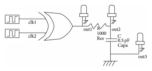
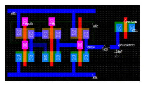
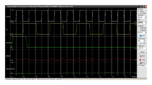
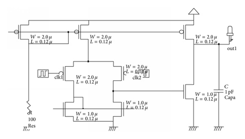
To get pure DC voltage along with rectifiers filters, the electronic circuits are also used. The second block of PLL is loop filter and it has two distinct functions. First, maintains stability, that is defined by describing the loop dynamics. This explains the response of the loop to uncertainties. The 2nd function is applied to the VCO control input which appears at the phase detector output. This frequency produces FM sidebands and modulates the VCO [10]. Other features of the PLL, for example, bandwidth, transient response, lock range, and capture range, can be controlled by LPF. The LPF is used to attenuate this energy, but it can also reject band. The low pass filter can be obtained by using a capacitor of large value and the capacitor is charged and discharged with the help of the switch resistance Ron. By the help of Ron.C delay a low pass filter can be created. Figure 6 depicts a CMOS schematic of phase detector with loop filter, Figure 7 shows layout, and Figure 8 shows output waveform.
2.3. Voltage Controlled Oscillator
As VCO is a source of varying output signal so the frequency of the output signal is regulated over a DC voltage range. The output signal can be a square wave or a triangular wave form. The oscillation frequency is controlled by the value of input voltage [11]. Figure 9 shows a CMOS circuit of VCO, Figure 10 shows layout, and Figure 11 shows output waveform.
2.4. Sigma-Delta Modulator
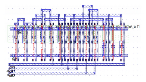
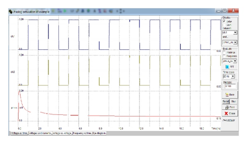
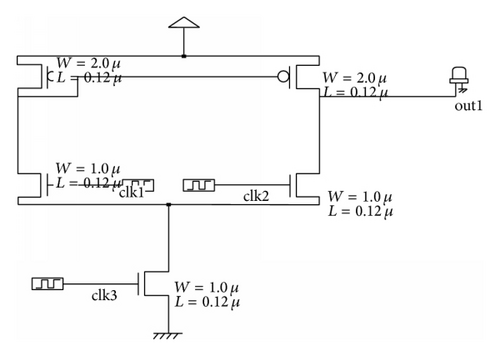
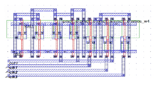
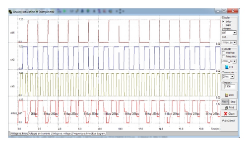
Sigma-delta modulation technique is used to convert high definition signals to low definition signals in digital domain. We designed sigma-delta modulator using 0.12 micrometer feature size and then the layout was obtained. The input is the aspired fractional number (n) and the output is the sum of quantization noise and a DC part [12, 13]. By the use of integer divider quantization noise was generated. Figures 12 and 15 show the CMOS circuit; Figures 13 and 16 show the layout of comparator and operational transconductance amplifier. Figures 14 and 17 show the output waveforms.
3. Conclusion
Power usage and heat dissipation are one of the biggest challenges of VLSI industry today. In order to design the low power consuming component, without making significant change in performance, the design of FNPLL frequency synthesizer was implemented and simulated. The optimized design was implemented to 0.12 micrometer technology. Using CMOS logic, the schematics were designed and verified functionally and then prefabrication layout was sketched. The simulation curves of the layouts reflected reduction in power consumption, for the optimized design.
Conflict of Interests
The authors declare that there is no conflict of interests regarding the publication of this paper.


