Design of Synthesizable, Retimed Digital Filters Using FPGA Based Path Solvers with MCM Approach: Comparison and CAD Tool
Abstract
Retiming is a transformation which can be applied to digital filter blocks that can increase the clock frequency. This transformation requires computation of critical path and shortest path at various stages. In literature, this problem is addressed at multiple points. However, very little attention is given to path solver blocks in retiming transformation algorithm which takes up most of the computation time. In this paper, we address the problem of optimizing the speed of path solvers in retiming transformation by introducing high level synthesis of path solver algorithm architectures on FPGA and a computer aided design tool. Filters have their combination blocks as adders, multipliers, and delay elements. Avoiding costly multipliers is very much needed for filter hardware implementation. This can be achieved efficiently by using multiplierless MCM technique. In the present work, retiming which is a high level synthesis optimization method is combined with multiplierless filter implementations using MCM algorithm. It is seen that retiming multiplierless designs gives better performance in terms of operating frequency. This paper also compares various retiming techniques for multiplierless digital filter design with respect to VLSI performance metrics such as area, speed, and power.
1. Introduction
High level synthesis is the process of converting behavioral description or an algorithm to structural level specification. In behavior description or an algorithm, the input and output behavior is described in terms of data transfers and operations without any implementation details. Structural description maps this data transfers and operations into combinational functional units and registers on to hardware. High level synthesis of DSP algorithms is very much useful as it reduces time to market window. Various optimization methods are available in literature for sequential synthesis [1]. Though synthesis of combinational logic has attained a significant level of maturity, sequential circuit synthesis has been lagging behind [2] in terms of frequency performance. DSP algorithms are repetitive and periodically iterations must be repeated to execute the computations [3]. Here, iteration period is the minimum time needed for computation and this is limited by critical path. Critical path can be altered by redistributing the delays such that functionality is preserved. Retiming algorithm [4] is used to redistribute the delays without altering [5] the functionality.
A great amount of research has been done on retiming [5, 6]. The retiming technique is the valuable optimization technique in problems of digital filters which can be represented as data flow graphs (DFGs). Efficient filter systems are needed to decrease the overall computation time since scientific applications can be recursive, nonrecursive, and iterative. Retiming transformation along with other high level transforms like multiple constant multiplication approach for filters in high level synthesis aids in reducing area of the filter circuit and most importantly decreases the clock period. Critical path and shortest path computations consume most of the time in retiming computation. The retiming minimizes the overall clock period, thereby increasing the clock frequency by reducing the filter critical path. In the general purpose processor where actual retiming vectors are computed for digital filters, the speed with which the retiming transformation is performed suffers since the entire transformation code will be written as software. Hence, FPGA based path solver architecture is designed in this paper which addresses the frequency issue in retiming and reduces the burden on general purpose processors.
A computer aided design (CAD) tool framework called DiFiDOT is developed which generates the synthesizable hardware descriptions of chosen digital filter with specified user constraints such as area, speed, and power. Since the digital filters are composed of adders/subtractors, multipliers, and delay elements, DiFiDOT picks the best choice of adders and multipliers as per users design constraints. Also, multiplication operation is expensive in terms of area, power, and delay. Exchanging multipliers with adders is advantageous because adders weigh less than multipliers in terms of silicon area [7]. Since the coefficients to be multiplied are known beforehand, the full flexibility of multiplier is not necessary in the design. So a multiplierless design in digital filter is proposed under multiple constant multiplications architecture and an option is included in DiFiDOT for generating multiplierless hardware descriptions. This significantly reduces the area of filters when compared to those designed using multiplier blocks. Here, sharing of partial terms in multiple constant multiplications (MCMs) concept [8] is used which reduces area and covers all possible partial terms that may be used to generate the set of coefficients in the MCM instance. For simulations, the authors have used some of ACM/SIGDA benchmark circuits.
2. Background
High level transformation techniques are applied to get optimal speed in sequential filter systems. For the designed optimization environment, input is considered as data flow graphs. This section introduces the data flow graphs (DFGs) and problem definitions and gives an overview on previously proposed retiming transformation algorithms with their drawbacks.
2.1. Data Flow Graphs (DFGs)
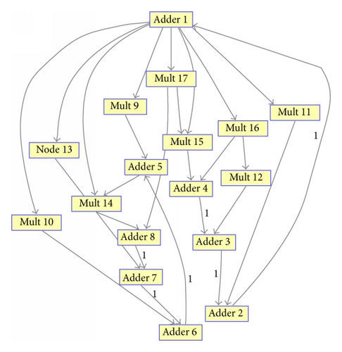
The second order elliptic filter block is as shown in Figure 1(a). The typical DFG for the filter is shown in Figure 1(b). For the designed optimization environment, the filter information is given in the form of matrices. There are two matrices which represent the filter information. The node-weight matrix represents node weights that are nothing but computation time unit delays in the filter graph. The computational complexity of the adder is O(n), whereas for multiplication it is O(n2) for two n digit numbers. Multiplication computation complexity is higher when compared to addition. Hence, in the present work, time delay considered for multiplication in retiming is twice that of addition. Incidence matrix defines the edge weights between all the nodes which represent connectivity information. The number of delay elements present in between the computation nodes (adder and multiplier) is considered as edge weight. If there are no delay elements and adder or multiplier node is directly connected to another node, then the edge weight will have zero value. The node weight matrix and incidence matrix are used as the inputs for optimization environment where high level transformations are applied to obtain performance improvement. The critical path and shortest path of the filter are computed for retiming which is one of the efficient optimization techniques to obtain a filter solution with reduced clock period which in turn increases the filter speed. The critical path can be obtained by observing Figure 1(b) DFG. The critical path is node 1 → 9 → 5 → 14 → 8.
- (i)
retiming using clock period minimization method,
- (ii)
retiming using register minimization method.
- (i)
Calculate , where n represents the number of nodes in the original DFG G and tmax is the maximum computation time of all the nodes in the DFG. Also compute the critical path which defines the required clock period of original graph.
- (ii)
A new DFG G* can be created from G. G* has the same nodes and edges as G. For each edge in G*, the edge weight is W*(e) = MW(e) − t(u), where W(e) is the edge weight of the same edge in G; t(u) is the computation time of the node initiating this edge.
- (iii)
We then apply the Floyd-Warshall shortest path algorithm to compute , which represents the shortest path from node U to node V.
- (iv)
From , WUV and DUV are calculated. If U ≠ V, then and . If U = V, then WUV and DUV = t(u). Here, t(U) and t(V) represent the computation times of node U and node V, respectively.
- (v)
We then find the maximum value of DUV and the minimum values of DUV. We check all the possible clock periods starting from maximum value of DUV to minimum value of DUV one by one. If we find a clock period that can give us a feasible solution, we stop and find the minimal clock period by solving for solutions critical path. The solution contains the retiming values for all nodes. Here, 4th-order low pass IIR elliptic filter is designed and retimed using the above mentioned clock period minimization algorithm. The retimed data flow graph with reduced clock period is shown in Figure 2.
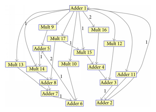
After applying retiming transformation to the filter, the critical path changes to 2 → 1 → 9.
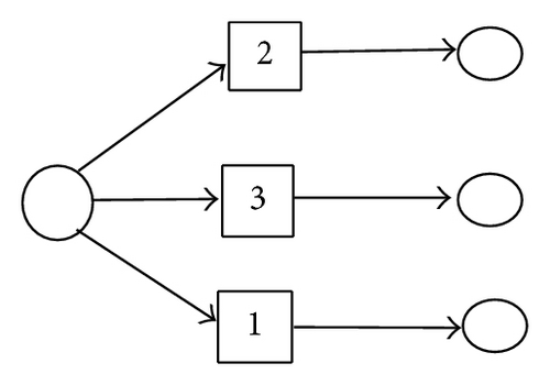
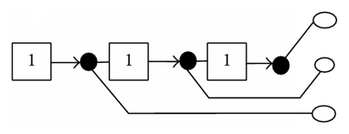
Since each delay element occupies about one-third of the binary adder, it is important to reduce the number of delay elements [11]. In retiming using register minimization, we can obtain the digital filter that uses minimum number of registers and satisfies the clock period constraints [15]. Here, forward splitting or register sharing [12] is used. If the node has several output edges carrying the same signal, the number of registers required to implement these edges is the maximum number of registers on any one of the edges. Consider Figure 3. The maximum number of registers required in Figure 3(a) is 6 whereas after register sharing, this gets reduced to 3 as shown in Figure 3(b).
- (i)
fan-out constraints: RV ≥ Wr for all V and all edges
- (ii)
feasibility constraints: r(U) − r(V) ≥ W(e) for every edge
- (iii)
clock period constraints: r(U) − r(V) ≥ W(U, V) − 1 for all vertices such that D(U, V) ≥ c, where c is the clock period.
- (i)
Use the gadget model of the graph to compute the cost function.
- (ii)
Calculate S′ by using shortest path Floyd-Warshall algorithm.
- (iii)
Compute D(U, V) and W(U, V) matrices from the original graph and S′ matrix.
- (iv)
Perform LP formulation such that the cost function gets minimized which is subjected to feasibility and clock period constraints.
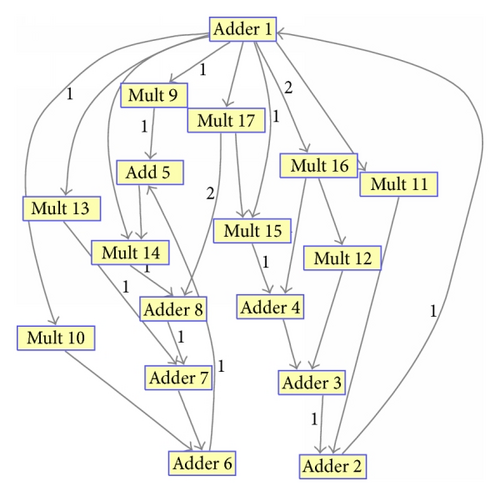
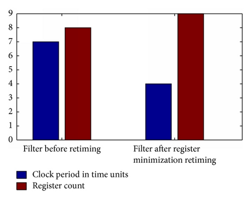
This LP problem is solved to obtain the retiming solution which minimizes the number of registers by satisfying the clock period. Figure 4 shows the DFG of 4th-order low pass IIR elliptic filter. It is observed that the register minimum retimed solution provides the filter solution with reduced register count for reduced clock period. However, in some cases, it is found that clock period minimization efficiency reduces in comparison to clock period minimization retiming technique as the priority is given to the register count. For the considered elliptic filter for a clock period of 4 units, it is found that the register count gets minimized to 9. After applying register minimization retiming transformation to the filter, the critical path changes to 1 → 9 → 5.
Problem Formulation. Critical path and shortest path solving contribute to most of the computation time in retiming.
Definition 1 (the path solver problem). Let S = {s0, s1, s2, s3, …, sk}, where k is the maximum number of feasible solutions available for retiming of a considered filter DFG. During retiming of digital filters in high level synthesis, the shortest path between the nodes must be computed for (k + 1) times where k is the number of feasible solutions available for the DFG which is nothing but unique entries in path delay D matrix. Similarly, the critical path must be computed for (k + 1). General purpose processors (GPPs) where retiming algorithm is implemented are fully programmable but are less efficient in terms of power and performance. Hence, the problem is to improve the performance and power of retiming using FPGA based path solvers. Further, along with retiming, high level transformation technique called automatic pipeline is applied to improve the filter speed.
Definition 2 (multiple constant multiplication in digital filters). For the considered filter coefficient constant T in the retimed filters, find the set of multiplierless operations {O1, O2, O3, …, On} with minimum number of addition, subtraction, and shift operations using multiple constant multiplier architecture to optimize the filter architecture further.
Definition 3 (optimization and automation of filter HDL). An environment needs to be developed to obtain HDLs of retimed filters in which user can choose different data path element architectures depending on the specifications. This reduces time to market and helps to evaluate a lot of hardware implementation trade-offs. Filter equivalence checking after applying high level transformation needs to be done which needs to be developed as a part of the optimization environment.
- (i)
k is an intermediate vertex on the shortest path,
- (ii)
k is not an intermediate vertex on the shortest path.
Let D be the incidence matrix with the graph edge weight information W initially. D is then updated with the calculated shortest paths; see Algorithm 1.
-
Algorithm 1
-
(1) n = # of rows in W, D0 = W
-
(2) for(k=1 to n)
-
(3) for(i=1 to n)
-
(4) for(j=1 to n)
-
(5) = min
-
(6) end for
-
(7) end for
-
(8) end for
-
(9) return Dn
The final D matrix will store all the shortest paths. This algorithm is extended for retiming of digital filters.
The multiple constant multiplication (MCM) problem is addressed in the literature [14] using either graph based methods or using common subexpression elimination method. In common subexpression elimination algorithm, all possible subexpressions are extracted for a variable. But this is possible only if it is defined as minimum signed digit and as canonical signed digit. Then the subexpression is found such that it can be shared by multiple constant multiplication values. In this paper, the above two concepts are extended for automatic pipelining and retiming of digital filters in high level synthesis. In all the digital filters, the filter coefficients are known beforehand. Hence, full flexibility of the multiplier is not necessary and we can make use of MCM designs. This method is more efficient when compared to shift and add multiplications as intermediate results can be shared which reduces the area of multiplierless implementation of digital filters. The sharing of intermediate result will provide potential area saving with increased filter order (Figure 5).

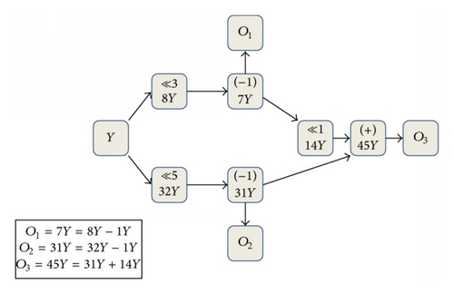
Consider the filter coefficient set which is to be used for the filter design given by T = {c1, c2, c3, …, cn}, we need to find the smallest set S given by {a1, a2, a3, …, s1, s2, s3, …, } where a (adders/Subtractors) & s (shifts) < S such that the set is made of adderssubtracters, shifters, and A operations. Here, shift operations also can be shared across multiple points so that the output set is optimum. Here Hcub algorithm [8] is used to generate corresponding DFG for the multiplier block implementing the parallel multiplications c1*x, c2*x, …, cn*x. The only operations used in the generated DAG and input design matrices are additions, subtractions, shifts, and negations. In this paper, performance of MCM based filter designs is further improved by combining this approach with retiming. The multiplierless filter circuit is further retimed to reduce the overall clock period which increases the clock frequency.
3. Design and Analysis
Each DSP filter block is associated with the critical path which limits maximum iteration period in the filter design [12]. This can be reduced by retiming where the clock period gets reduced and increases the clock speed. To reduce the critical path, we need to find the original critical path of the circuit using critical path solving algorithm and then apply retiming transformation to digital filter. While retiming, shortest path algorithm is required for solving the system inequalities. FPGAs are nothing but set of configurable logic blocks with configurable interconnects. Designer can program it to work like a specific hardware. These give great speedup over general purpose processors for many long running algorithms. Hence, for high performance systems, FPGAs become a better choice. In the present work, path solvers are implemented on FPGA to increase the performance.
3.1. Critical Path Solver Algorithm: Design and Analysis
-
Algorithm 2
-
(1) //Algorithm for computing the critical path
-
(2) Input: a DFG of G = (V,E,t,d) Where c is the
-
(3) computation time of the node and d
-
(4) is the initial delay on edge E
-
(5) Output: Critical path C
-
(6) Sort all the vertices topologically in the DFG G
-
(7) with v fallowing u
-
(8) if there is a zero delay edge from u → v
-
(9) For all vertices from the sorted list
-
(10) If non zero delay on the edge E in G then
-
(11) γi = tv
-
(12) else
-
(13) γi = tv + max(γi) ∈ edge e : u → v in G with de = 0
-
(14) end if;
-
(15) γ = γ1, γ2, …,γm
-
(16) where m = number of entries in the topologically sorted list
-
(17) end for;
-
(18) compute γ = max{γ}
- (i)
The filter network graph is considered as input to critical path solver algorithm.
- (ii)
All the zero-weight edges in the network graph are found and a matrix of their source and destination nodes is formed.
- (iii)
For each row in the above matrix, if the destination node of any zero-weight edge path is the same as the source node of the zero-weight edge path, the two paths are joined. This step is repeated to obtain a matrix whose rows will have nodes of all the possible zero-weight edge paths in the graph.
- (iv)
The computational time of each zero-weight edge path from this matrix is calculated.
- (v)
The zero-weight edge path with the greatest computational time is found. This is the critical path and its computational time is the critical path delay.
A critical path solver algorithm is designed in the present work on FPGA. The state diagram for the implemented critical path solver is given in Figure 6. In S0, the filter graph or matrix is given as input to the critical path solver module. Since HDL does not provide a method to represent infinity, some number, say 255, can be chosen which is always greater than any other weight in the incidence matrix. Also since edge weight 0 is a valid input, any negative number, say −1, can be used to denote the uninitialized matrix element. In state S1, all the zero weight edges in the DFG are found along with their source and destination nodes and are stored in a matrix called zero_weight_path. The zero_weight_path matrix contains two columns. The first column contains the source node of a directed zero-weight edge while the second column has the destination node of the directed zero-weight edge. Simultaneously, we will keep a count on the number of zero-weight edges.
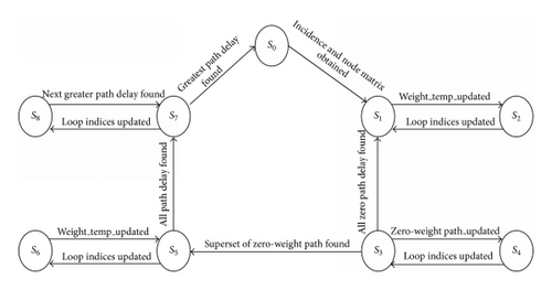
The state S2 is provided to enable looping action and for updating of all the signals. In state S3, in each row of zero_weight_path matrix, the module will find the next node with a zero-weight edge connecting it to the node in the previous column (if it exists). Thus, if the destination node in any zero-weight path is same as the source node in another zero-weight path, the two paths are concatenated, that is, if the destination node in path a is the source node in path b, then we make the destination node in b as the destination node of a. The state S4 is provided to enable looping action and for updating all the signals. At the end of this state, the zero_weight_path matrix will contain only those superset paths that are a superset of the remaining zero weight paths. In state S5, the module calculates the sum of all the node weights through each of these paths. State S6 is provided for looping action and for updating all signals.
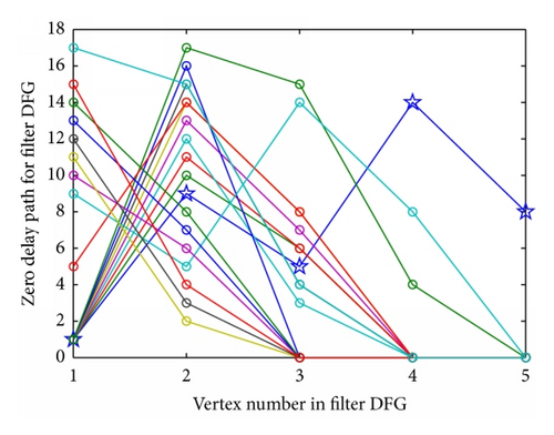
In state S7 the path with the highest node weights sum is found, which is the critical path of the DFG. All the nodes in this path are then stored in order in a matrix called the critical path matrix. These signals, in this matrix, are output as the critical path. The state S8 is provided to enable looping action and for updating all the signals. The state machine then goes back to state S0 and awaits new inputs. Next, algorithm to find the shortest path between two nodes in a graph is described. For retiming technique in high level synthesis, we need the shortest path to solve system of inequalities. It is seen that time needed to compute critical path on FPGA is reasonably less when compared to computation on general purpose processor. This also reduces the retiming computation time. The zero delay paths are computed for 4th-order elliptic filter shown in Figure 7. The highlighted path delay is from1 → 9 → 5 → 14 → 8 where nodes 1,5, 8 are adders and 9,14 are multipliers. Maximum path delay which is highlighted is considered to be the critical path.
3.2. Shortest Path Solver Algorithm and State Diagram
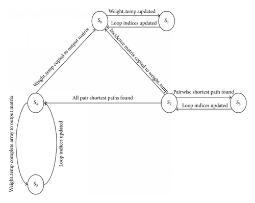
Let D(u, v) be the maximum delay between nodes u and v and let T(u, v) be total computation time of zero delay path from u to v. We can check the condition T(u, v) − min{t(u), t(v)}>{derived clock period} then select those paths to retime so that computation time in this path can be reduced. We have to retime the edges by constructing system of linear inequalities. This can be done using Floyd-Warshall shortest path algorithm (Algorithm 3). This can be used for retiming the graph further (Figure 6).
-
Algorithm 3
-
(1) Algorithm for computing the shortest path
-
(2) Input: a DFG of G = (V,E,t,d) Where c is the computation time of the node and d
-
(3) is the initial delay on edge E
-
(4) Output: All pair shortest path matrix M
-
(5) for i = 1 to N
-
(6) for j = 1 to N
-
(7) if i = j, then
-
(8) M[i,j] = (0,0)
-
(9) else M[i,j] = inf
-
(10) end for
-
(11) end for
-
(12) for all the edges e : u → v, M[u, v] = d for edge e
-
(13) for k → 1 to N
-
(14) for i → 1 to N
-
(15) for j → 1 to N
-
(16) if M[i, j] > M[i, k] + M[k, j]
-
(17) M[i,j] = M[i,k] + M[k,j]
-
(18) end for
-
(19) end for
-
(20) end for
-
(21) Output shortest path matrix M
3.3. Multiplierless Digital Filters
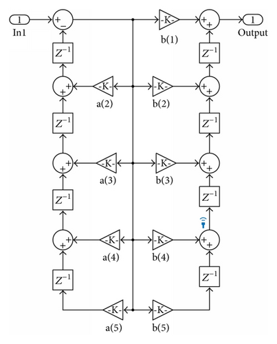
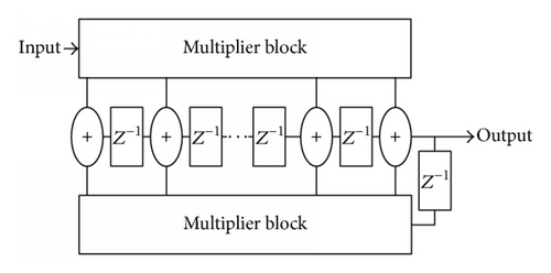
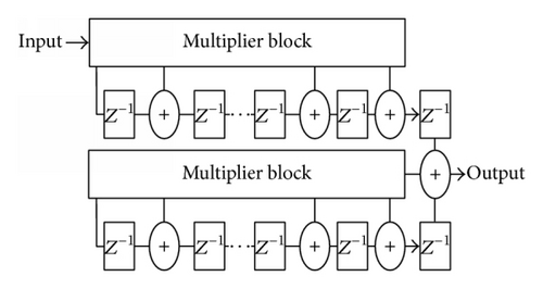
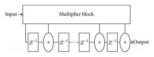
The digital FIR filters and the transposed IIR filters will have block of multipliers in the filter structure. This is shown in Figure 9.
- (i)
maximum benefit,
- (ii)
cumulative benefit.
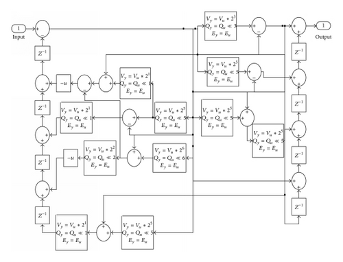
Here, cumulative benefit heuristic adds up the weighted benefit considering all the targets. With this particular method, target set is calculated. With this target set, filter graph which is multiplierless MCM based can be designed. It is found that multiplierless designs reduce the combinational path delays and due to sharing of intermediate results in the MCM approach. The performance can be further improved by retiming Gi to give Gr. These two different optimization techniques reduce the combination delay and critical path without changing the functionality which further increases the clock speed. The 4th-order lattice filter with multiplierless MCM concept using Hcub algorithm is shown in Figure 10. It is seen from the synthesis that combination delay is reduced. It is further retimed either for clock period minimization or register minimization. This requires solving a set of linear inequalities with a computation complexity of O(n3) where n is the number of nodes using the Floyd-Warshall algorithm, where n is the number of nodes [8]. The clock period minimization and register minimization retiming algorithms are designed and implemented with FPGA based path solvers which reduces computation time when compared to previous methods [8, 16] to design multiplierless digital filters.
The algorithm starts by building a new graph from the original DFG. The new graph can give us a set of inequalities called the critical path constraints. The original DFG also presents a set of equalities called the feasibility constraints. A constraint graph can be built from the critical path constraints and the feasibility constraints. The retiming values for each node can be derived by applying a Floyd-Warshall shortest path algorithm to the constraint graph. The weight for each edge in the retimed DFG can be calculated using the original weight and the retiming values of the two nodes connected by this edge. The improvement in the clock frequency is shown in Figure 11. Here, 4th-order lattice filter is considered. Design1 is the filter with multipliers and without retiming, Design2 is multiplierless MCM based filter without retiming, Design3 is the filter with multipliers with retiming, and Design4 is multiplierless MCM based lattice filter with retiming. The maximum operating frequency of the filter has increased by 19.6% in multiplierless MCM approach as multipliers will get eliminated and get replaced by adders which have much less computation delay. Further, it is observed that by combining this approach with retiming, operating frequency increases by 35.4% which is a significant increase. However, with this technique, the number of registers increases from 9 to 11.
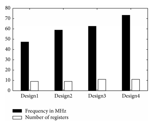
Hence, when the filter is designed without multipliers (that is using only adders/subtractors and shifters) along with the retiming technique, operating clock speed is found to increase which gives a greater speed advantage for the design under consideration.
3.4. Computer Aided Design Tool
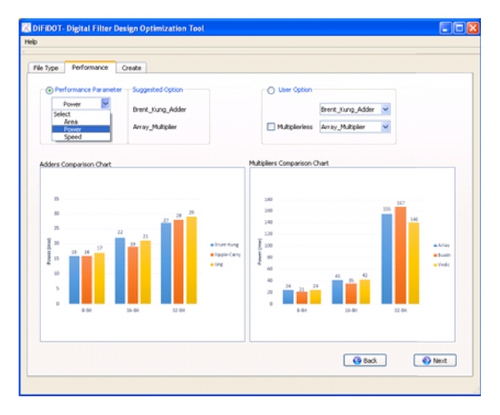
This section presents the DiFiDOT tool which is designed as the part of research work. Initially, the design of filters is performed using retimed architecture where user can choose either clock period minimization or register minimization retiming as per his need. The tool will retime the digital filter by optimizing the critical path and generate verilog/VHDL based filter RTL for the same. The performance of a filter can also be increased by varying the choice combinational adder and multiplier elements in the RTL filter description. A graphical user interface (GUI) is created in DiFiDOT using Nokia QT 4.8.0 for component selection and optimization of digital filters. Here, user has to input the HDL file which was automatically generated after retiming for further component optimization. The user can choose adders and multipliers of his choice according to the design requirements for the retimed digital filters using drop down menu. The original HDL is automatically modified with respect to the components chosen which is again synthesizable and is given as the output to the user. This easy to use GUI helps designer to optimize and generate digital filter RTL with the adder and multipliers of his choice. With this, designer can conveniently explore the solution space of possible architectures and also analyze the trade-offs in the energy-area-performance space [20]. The different adder and multipliers considered in the tool are as below.
Multiplier Architecture. The most critical function carried out by any filter is multiplication. Digital multiplication [19] is the most extensively used operation in signal processing. Innumerable schemes have been proposed for realization of the operation. In this paper, we consider three types of multipliers.
Radix 4 Booth Multiplier. It has the advantage of lesser area and faster multiplication compared with array multiplication. Radix 4 Booths Algorithm can scan strings of three bits and is converted depending on modified Booth encoder table. The design of Booths multiplier in this project consists of four Modified Booth Encoders (MBE), four sign extension correctors, four partial product generators (comprises of 5 : 1 multiplexer), and finally a Ripple carry Adder. This Booth multiplier technique is to increase speed by reducing the number of partial products by half. Since a 32-bit booth multiplier is used in this project, there are only sixteen partial products that need to be added instead of 32 partial products generated using conventional multiplier.
Vedic Multiplier. It is used for faster multiplication operations in higher order bits. It has less combinational path delay [21] compared with others when the bit size is higher. However, it consumes more area than Booth multiplier and array multiplier. The multiplier is based on an algorithm Urdhva Tiryakbhyam (vertical & crosswise) Sutra which is a general multiplication formula applicable to all cases of multiplication. It means vertically and crosswise. It is based on a novel concept through which the generation of all partial products can be done with the concurrent addition of these partial products. The speed advantage is compromised with increased power dissipation and area. Due to its regular structure, layout of this can be easily generated.
The different multipliers are designed for different bit sizes and results are compared. This is as shown in Table 1.
| Type of multiplier | Delay in ns | Power in mW | Number of LUTs | ||||||
|---|---|---|---|---|---|---|---|---|---|
| 32 bit | 16 bit | 8 bit | 32 bit | 16 bit | 8 bit | 32 bit | 16 bit | 8 bit | |
| Array | 76.1 | 39.9 | 21 | 21 | 11 | 7 | 1519 | 375 | 91 |
| Booth | 86.1 | 27.99 | 14.9 | 25 | 15 | 12 | 1277 | 317 | 77 |
| Vedic | 70.7 | 39.02 | 24.4 | 28 | 18 | 12 | 2378 | 565 | 126 |
3.5. Adders
In this paper, qualitative evaluations of the classified binary adder architectures are performed since adder is another basic component of FIR filter. Here, Ripple-carry adder, BruntKung adder, and Ling adder are considered to emphasize the performance properties. Adders affect the critical path delay and area.
Ripple Adder. It is the basic adder type. This is composed of cascaded full adders for n-bit adder. It is constructed by cascading full adder blocks in series. The carry-out of one stage is fed directly to the carry-in of the next stage. For an n-bit parallel adder, it requires n full adders.
| Type of | Delay in ns | Power in mW | Number of LUTs | ||||||
|---|---|---|---|---|---|---|---|---|---|
| adder | 32 bit | 16 bit | 8 bit | 32 bit | 16 bit | 8 bit | 32 bit | 16 bit | 8 bit |
| Ling | 8.854 | 15.24 | 20.21 | 6 | 9 | 18 | 23 | 53 | 107 |
| BrentKung | 10.4 | 18.39 | 25.83 | 4 | 6 | 9 | 15 | 30 | 63 |
| Ripple | 12.12 | 20.63 | 37.6 | 2 | 7 | 14 | 9 | 18 | 36 |
In the GUI, an option is crested for particular adder and multiplier combination also depending on whether the performance parameter is speed, power, or area and also based on the bit size. For example, if the design constraint that user chooses is power then Brent-Kung adder and array multiplier pair are considered as the best combination to implement the filter in the design optimization GUI. User can also choose any one of his choice among area, power, or speed constraint for digital filter HDL generation. Along with this, an option is created for multiplierless filter design description as well based on MCM approach. It is seen that the retimed MCM circuits outperform the existing MCM methods [23] in terms of speed. Using this tool, user can design retimed digital filter which has combination elements of his choice which are specific to particular design constraint and generate the RTL for the same. The obtained RTL can be synthesized with any of the commercially available synthesis tools. The GUI designed is shown in Figure 12. A Hcub based algorithm is considered for implementing MCM blocks in multiplierless digital filters for specific user defined option in DiFiDOT. Since all the multipliers can be realised as a block in transposed IIR and FIR filters, they are well suited for MCM implementation. After retiming, the multiplier blocks in digital filter can be replaced by a block constructed by adderssubtractors, negation operations, and shifters in multiplierless design approach. The generated MCM block will have tree depth in terms of different components and this depth in our work is assumed to be infinity. The tool DiFiDOT automatically generates the HDL of retimed digital filter which is under consideration which can be directly synthesizable. With this tool and automation, even if reiteration of the design cycle happens due to specification change, time taken to reiterate is very little.
4. Experimental Results
This section is divided in to three parts: the first part presents the results of retiming with FPGA based path solvers, second part presents comparison of various retiming techniques, and third part presents the timing results of retimed filter structures with MCM blocks.
4.1. Results on Path Solvers for Retiming
The main idea of implementing path solver algorithms on FPGA is to speed up the results for retiming purposes. The inputs are passed to the FPGA based path solver block by a processor where retiming algorithm is implemented. The computations are performed in FPGA based block and shortest path along with critical path is computed and communicated back to the processor where retiming will be performed. For comparison, a set of designs is used to test the path solver algorithms. The designs are a diverse set of DSP functions of varying complexity which includes recursive and nonrecursive filter structures. The considered target device for path solver implementation is Spartan6 family based XC6SSLX16. The simulation and synthesis of path solvers are performed using Xilinx ISE tool suit and the synthesis and the timing results after synthesis are shown in Table 1. The FPGA based path solver computes critical path and shortest path and communicates the results to the processor where retiming is performed. This reduces the burden on main processor (Table 3).
| Path solver name | Device utilization summery | Timing summery | Max. frequency (Hz) | |||
|---|---|---|---|---|---|---|
| Logic utilization | Used | Min period in ns | Setup time in ns | Hold time in ns | ||
| Critical path solver | Number of slices | 5804 | 9.068 ns | 15.72 ns | 6.141 ns | 110.277 |
| Number of LUTs | 10462 | |||||
| Number of slice Flipops | 3664 | |||||
| Shortest path solver | Number of slices | 4147 | 14.089 ns | 10.477 ns | 4.114 ns | 70.978 |
| Number of LUTs | 7511 | |||||
| Number of slice Flipops | 1496 | |||||
Here, various IIR and FIR filters have been considered to analyze the FPGA based path solvers and execution time of FPGA design is compared with the general purpose processor (GPP) based design. Also, GPP denotes the required CPU time in milliseconds of the path solver to find the minimum solution on a PC with Intel Pentium 5 machine at 2 GHz and 4 GB of memory. FPGA based design solves for critical path and shortest path in very less time when compared to the general purpose processor based path solvers. The time taken by the FPGA path solvers is compared in Table 4 to the time taken by the algorithms run using general purpose processor with Matlab environment. The time overhead needed for general purpose processor where retiming algorithm is implemented in MATLAB to communicate with the FPGA based path solvers is around 210 ns for each computation. Including this, the time gain achieved is quite substantial when compared to designs without FPGA based path solvers. These time gains are good and can really help speed up the results, which is crucial for retiming.
| Filter order | Critical path solver algorithm | Shortest path solver algorithm | ||||||
|---|---|---|---|---|---|---|---|---|
| IIR filter | FIR filter | IIR filter | FIR filter | |||||
| FPGA based | GPP based | FPGA based | GPP based | FPGA based | GPP based | FPGA based | GPP based | |
| (ns) | (ms) | (ns) | (ms) | (ns) | (ms) | (ns) | (ms) | |
| 2 | 4.60 | 13.8 | 9.06 | 12.83 | 2.78 | 3.05 | 3.05 | 12.80 |
| 4 | 15.71 | 15.78 | 16.31 | 14.46 | 3.68 | 13.91 | 13.91 | 13.19 |
| 6 | 29.98 | 19.18 | 19.23 | 15.47 | 3.98 | 15.42 | 15.42 | 17.31 |
| 8 | 31.62 | 21.90 | 29.71 | 16.42 | 4.52 | 25.23 | 25.23 | 32.94 |
| 10 | 39.81 | 26.27 | 36.53 | 18.61 | 5.36 | 42.93 | 42.93 | 45.34 |
| 12 | 46.72 | 31.42 | 43.28 | 23.52 | 6.71 | 55.34 | 55.34 | 51.61 |
4.2. Comparison of Clock Period Minimization and Register Minimization Retiming Technique
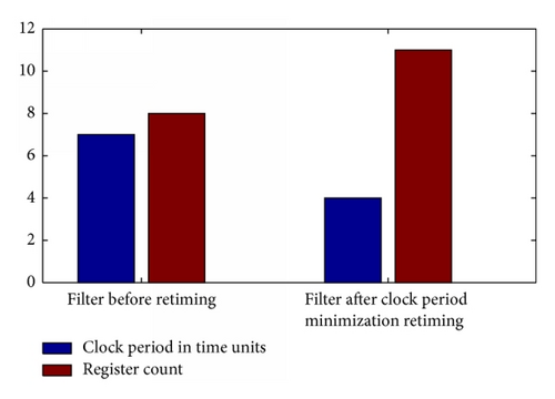
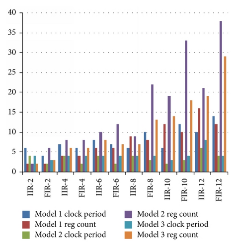
Different filter structures are designed and they are compared with respect to the clock period and register count before and after retiming. It is observed that after retiming, the clock period gets reduced. The register count gets altered depending on the filters iteration bound. Here, three models are considered. Model1 is the filter without retiming and with adder, subtractor, multiplier, and delay elements. Model2 is retimed filter based on clock period minimization algorithm. Model3 is retimed filter based on register minimization algorithm. After retiming, the results are compared with the original circuit [24]. The comparison results are shown in Figure 13. After retiming, the finite state machine is extracted from the retimed circuit and it is compared with original circuit for its functionality. It is observed that clock period minimization retiming algorithm is efficient in terms of reduction critical path, thereby increase in the clock frequency. However, this might increase the register count. In register minimization retiming [18], the number of registers after retiming will be reduced while compromising the clock period.
4.3. Area, Power, and Timing Results for Digital Filter before and after Retiming for Different Adder and Multiplier Combinations
The FIR and IIR filters are designed with respect to different adders and multipliers combinations. As an application example, IIR and FIR filters [25] of order 10 are considered. Table 5 shows the results of FIR/IIR filters before and after retiming for particular adder and multiplier combinations. User can choose any adder and multiplier for the filter circuit depending on the design requirement. In the GUI, particular adder and multiplier combination is considered depending on whether the performance parameter is delay, power, or area and also based on the bit size. If user does not want to use these in built combinations, user can choose any one of his choice among the available for FIR/IIR digital filter HDL generation with specific combinational components.
| Filter block | Adder/multiplier combinations | Before retiming | After retiming | ||||
|---|---|---|---|---|---|---|---|
| Number of LUTs | Max. operating freq in MHz | Power in mw | Number of LUTs | Max. operating freq in MHz | Power in mw | ||
| IIR-10 | Brentkung Adder/Array Multiplier | 2222 | 62.526 | 99 | 2411 | 76.977 | 89 |
| Ling Adder/Vedic Multiplier | 2214 | 69.702 | 112 | 2193 | 95.381 | 94 | |
| Ripple carry Adder/Booth Multiplier | 2146 | 50.861 | 114 | 1809 | 65.248 | 95 | |
| FIR-10 | Brentkung Adder/Array Multiplier | 1736 | 62.526 | 94 | 1811 | 99.43 | 85 |
| Ling Adder/Vedic Multiplier | 2162 | 72.493 | 111 | 2271 | 100.72 | 95 | |
| Ripple carry Adder/Booth Multiplier | 1637 | 52.302 | 105 | 1615 | 71.345 | 87 | |
4.4. Results for Optimization of Latency, Multiplier Components, and Power in Multiplierless Multiple Constant Multiplication Based Filter Designs Using Retiming Algorithm
- (i)
Model 1: Filter with adder, multiplier, and delay elements.
- (ii)
Model 2: Filter based on multiplierless multiple constant multiplication approach.
- (iii)
Model 3: Retimed multiplierless multiple constant multiplication based filter.
| Filter block | Adder multipliers Flipflops | DelayMax Freq in MHz | Power in Watts | ||||||
|---|---|---|---|---|---|---|---|---|---|
| Model 1 | Model 2 | Model 3 | Model 1 | Model 2 | Model 3 | Model 1 | Model 2 | Model 3 | |
| FIR-2 | 5/2/3 | 5/0/3 | 5/0/4 | 51.54 | 192.14 | 340.62 | 0.056 | 0.063 | 0.065 |
| FIR-4 | 10/3/5 | 11/0/5 | 11/0/8 | 59.41 | 108.41 | 222.04 | 0.047 | 0.057 | 0.060 |
| FIR-6 | 7/2/7 | 17/0/7 | 17/0/14 | 62.91 | 67.64 | 259.47 | 0.051 | 0.062 | 0.064 |
| FIR-8 | 15/5/9 | 22/0/9 | 22/0/16 | 54.82 | 65.92 | 117.91 | 0.054 | 0.058 | 0.065 |
| FIR-10 | 18/6/11 | 25/0/11 | 25/0/11 | 48.22 | 56.37 | 100.72 | 0.058 | 0.061 | 0.063 |
| FIR-12 | 20/7/13 | 29/0/13 | 29/0/13 | 46.34 | 54.86 | 193.40 | 0.060 | 0.063 | 0.067 |
| IIR-2 | 9/4/3 | 11/0/3 | 11/0/3 | 55.03 | 75.53 | 89.10 | 0.047 | 0.050 | 0.050 |
| IIR-4 | 16/7/5 | 20/0/5 | 19/0/6 | 22.78 | 113.88 | 151.65 | 0.059 | 0.062 | 0.063 |
| IIR-6 | 24/11/7 | 35/0/7 | 35/0/8 | 38.71 | 42.54 | 53.142 | 0.051 | 0.059 | 0.058 |
| IIR-8 | 30/11/10 | 33/0/10 | 33/0/7 | 29.46 | 70.14 | 110.21 | 0.044 | 0.064 | 0.081 |
| IIR-10 | 37/16/13 | 54/0/13 | 54/0/14 | 36.43 | 48.85 | 95.381 | 0.051 | 0.067 | 0.085 |
| IIR-12 | 42/20/17 | 63/0/17 | 63/0/19 | 39.73 | 50.74 | 101.52 | 0.063 | 0.071 | 0.088 |
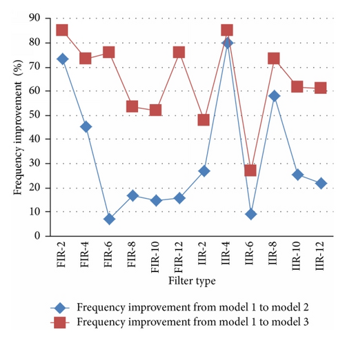
All the three models are compared for the performance parameters such as area, power, and delay. Here, it is ensured that functionality of the circuits after and before retiming is retained. The frequency improvement seen for different filters by considering the above models is given in Figure 14. It is seen that frequency parameter is improved when retiming technique is applied for multiplierless MCM based digital filters.
5. Application Example
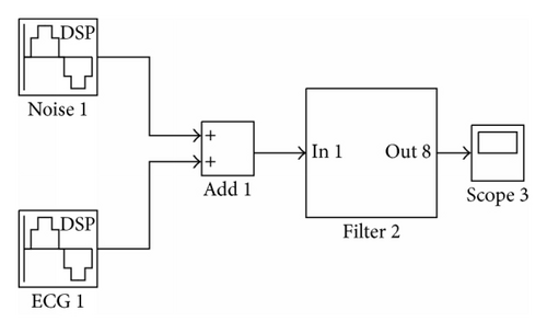
The electrocardiogram (ECG) is the most commonly used diagnostic method for heart diseases. Good quality ECG is utilized by physicians for interpretation and identification of physiological and pathological phenomena. ECG recordings are often corrupted by high-frequency noises, such as power-line interference, electromyography (EMG) noise, and instrumentation noise. An ECG is usually affected by the 50/60 Hz noise in the power supply lines. This noise can be eliminated by using a digital filter. The model is constructed in matlab and tested for ECG signals for removing the noise. The constructed model uses retimed multiplierless MCM filter which is implemented on FPGA and tested for ECG signal which is corrupted by power-line noise. The filter efficiently filters out the noise and outputs the clean ECG signal. The ECG noise removal block using the optimized filter structure is shown in Figure 15.
6. Conclusions
In this paper, we introduced the retiming approach for designing multiplierless MCM based digital filters with speed and area as the constraint. The implementation cost at the gate level is reduced by using addition, subtraction, and shift operations instead of multiplication and by using register sharing and register minimization retiming algorithm approach. Since there are still instances with which multiplierless designs can not cope, we also proposed the combination of adder and multiplier blocks which can be used in retimed filter design which is applicable for specific VLSI design constraint such as power, area, and timing. This yields the optimal clock speed and gate-level area in design and implementation of digital filters. This paper also introduced the design architectures for the digital filter and a CAD tool for the realization of retimed digital filters which can be either multiplierless MCM based or with adder/subtractor, multiplier, and delay elements. This tool directly gives the synthesizable filter RTL which reduces lot of designers’ time and effort in the design cycle. The experimental results indicate that the retiming algorithm efficiency can be further increased by using FPGA based path solver algorithms proposed in this paper. It was shown that the realization of path solver architectures for solving critical path and shortest path in retiming computation and communicating the results to the processor where retiming algorithm is implemented yields significant increase in computation time gain when compared to the filter designs for which path solver algorithms are implemented as a part of retiming algorithm in the processor. It is observed that a designer can find the synthesizable digital filter RTL that fits best in an application.
Conflict of Interests
The authors declare that there is no conflict of interests regarding the publication of this paper.


