Device Modeling of the Performance of Cu(In,Ga)Se2 Solar Cells with V-Shaped Bandgap Profiles
Abstract
The effect of Cu(In,Ga)Se2 (CIGS) with V-shaped bandgap on device performance is investigated in detail. A series of Ga/(In+Ga) ratio are set to study the influence of V-shaped bandgap profile on the electricity of CIGS thin film solar cells. The modeling of device current density-voltage (J-V) curve and bandgap grading profile corresponded well to measurement results. Detailed characteristic and modeling results show that an increased gradient of bandgap from valley to the buffer layer CdS will result in a barrier and lead to an enhanced recombination in the valley. This phenomenon can be modified by the back electric field resulting from a gradient bandgap from valley (bandgap minimum) to the Mo back contact. These results indicate CIGS-based solar cells can achieve higher performance by optimizing the V-shaped bandgap profile.
1. Introduction
Nowadays, it is an important issue to improve the conversion efficiency of thin-film solar cells. Impressively, the record conversion efficiency of thin-film Cu(In,Ga)Se2-based solar cells are to date over 20% [1]. The major advantage of the CIGS-based solar cell is that the quaternary material system can attain a variable bandgap energy and lattice parameters by varying the Ga/(In+Ga) ratio [2]. Chalcopyrite CIGS is reported to have an adjustable bandgap from 1.01 eV (CIS) to 1.636 eV (CGS) by changing the gallium content from 0 to 1 [3]. However, only the position of the conduction-band edge will be affected when changing the CIGS bandgap [4, 5]. The latest reported high efficiency CIGS solar cell uses three- or multistage evaporation processes to prepare CIGS absorber layer with a double-graded bandgap profile, a higher gallium content towards the back and the front of the CIGS absorber layer, and a notch of low gallium content in between [6]. From the other earlier research, the influence of the decreasing of gallium content from the buffer layer towards the notch of the absorber can enhance the electrons generated within the space-charge region [7]. Furthermore, the potential benefit of the Ga content increases from notch towards the back contact induces a back-surface field in the conduction band, which causes electrons to drift away from the rear contact and thereby reduces the recombination at the back contact [8]. As mentioned above, it is an excellent method to provide a variable bandgap of CIGS and obtain higher open circuit voltage and efficiency by using gallium to replace partial of indium.
However, it is hard to understand the benefits and effects of “grading” by studying the actual devices. Therefore, in order to understand how “grading” can improve cell performance, a novel approach is to use numerical modeling [9, 10]. In this paper, we investigate the influence of the Ga content numerically in the CIGS solar cells by modeling and device simulation. The amount of Ga doping is fixed in order to avoid the influence of open-circuit voltage by different gallium content, and we introduce different distributions in absorber layer to analyze and investigate the effect of different type of gradient bandgap.
2. Simulation
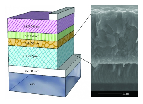
The device characteristics of the CIGS solar cells are studied numerically using the APSYS simulation program, which was developed by Crosslight Software Inc. [11]. The APSYS simulation program can deal with electrical properties by solving several interwoven equations including the basic Poisson’s equation, drift-diffusion equations, photon rate equation, and scalar wave equation. To investigate the effect of bandgap grading in a CIGS solar cell, physical parameters of CIGS solar cells needed for electrical modeling are obtained from measurements and earlier literatures to construct the accurate model [12–14]. Table 1 lists the parameters used in the numerical model. In the simulation, the model consists of several layers including 500-nm-thick AZO transparent conductive oxide layer, 50-nm-thick intrinsic ZnO layer, 50-nm-thick CdS buffer layer, and 2-μm-thick CIGS absorber layer. All simulations have been performed under an AM 1.5G light spectrum.
| AZO | i-ZnO | CdS | CIGS | |
|---|---|---|---|---|
| Thickness (nm) | 500 | 50 | 50 | 2000 |
| ε | 9 | 9 | 10 | 13.6 |
| μn (cm2/Vs) | 50 | 50 | 10 | 300 |
| μp (cm2/Vs) | 5 | 5 | 1 | 30 |
| NA (1/cm3) | 0 | 0 | 0 | 8.E + 16 |
| ND (1/cm3) | 1.E + 20 | 1.E + 17 | 5.2E + 16 | 0 |
| Eg (eV) | 3.3 | 3.3 | 2.4 | grading |
| χ (eV) | 4 | 4 | 3.75 | 3.89 |
- ε, dielectric constant; μn, electron mobility; μp, hole mobility; NA, effective density of states in conduction band; ND, effective density of states in valence band; Eg, bandgap energy; χ, electron affinity.
In order to confirm the validity of our model, the results of numerical analysis are compared with device measurement. Afterward two different types of absorber layer are discussed in detail. In the first type, we fix the Ga doping and vary bandgap notch depth (minimum bandgap). Whereas, the second type keeps bandgap notch depth unchanged but with different front grading (linear variation from notch increase towards the front side). After that, the electrical properties such as current density-voltage (J-V) curves, electric field intensity, and recombination intensity are investigated.
3. Results and Discussion
The cell structure and cross-sectional scanning electron microscopy (SEM) photographs of typical CIGS/Mo structure fabricated on Mo-coated soda-lime glass substrate are shown in Figure 1(a). SEM images show a reduction in grain size with increasing Ga content from top to bottom of absorber layer, which agrees well with the results by other groups [17]. In Figure 1(b), the J-V curve from simulation is compared with experimental data, and inset shows the bandgap grading (Ga content) in absorber layer. From SIMS measurement result, one can find that bandgap shows a “V”-shaped grading (see inset in Figure 1(b)) with the minimum gap locating at 150 nm from the CdS/CIGS surface (located at x = 0 nm). All measurements and simulations are set under room temperature. At the same time, the simulation of J-V curve with V-shaped grading is corresponding well to measurements. This result indicates that the baseline parameters used in the model are in line with the physical properties of actual device.
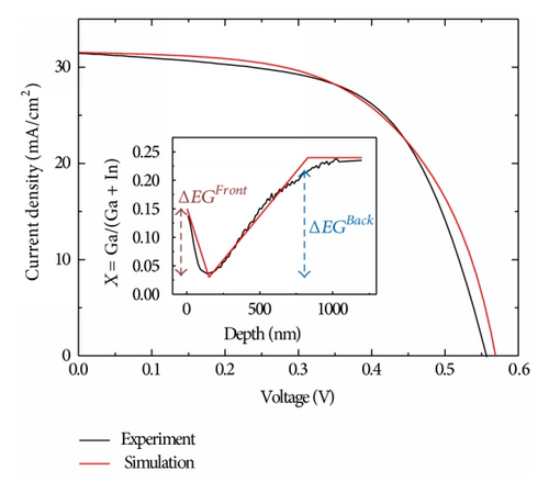
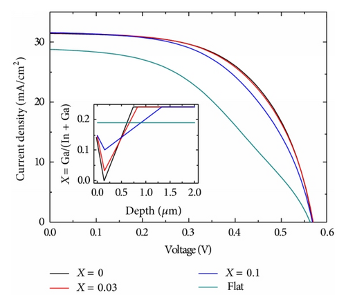
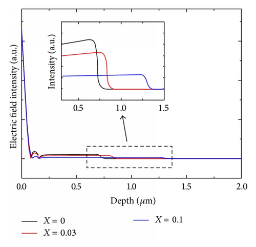
It has been well known that Ga doping will not only change the CIGS bandgap but also obtain different open circuit voltage. The parameters are shown in Table 2. Therefore, in the simulation, we compare the samples with same amount of Ga contents in the absorber layer but different minimum bandgap in a distance of 150 nm from the CdS/CIGS surface as shown in inset of Figure 2(a). In addition, we also take the case with no V-shaped grading into consideration. The inset of Figure 1(b) shows the difference between the bandgap minimum and maximum close to the back contact and CdS buffer layer, which is defined as ΔEgBack and ΔEgFront, respectively. From Figure 2(a), the fill factor of photovoltaic device will increase as the depth of valley (minimum gap) in the absorber layer increases. As expected, more recombination might happen in the valley when the valley became deeper. Simultaneously, a stronger electric field is created to provide the carriers more energy to drift out the space charge region (SCR) as the ΔEgBack becomes larger as shown in Figure 2(b). In this way, the carrier collection will be increased and also the fill factor. From these results we can speculate that the positive ΔEgBF (ΔEgBF = ΔEgBack − ΔEgFront) can reduce the recombination in the valley of absorber layer.
| Samples | Voc (V) | Jsc (mA/cm2) | F.F. | η (%) | Ga/(Ga + In) | |
|---|---|---|---|---|---|---|
| X = 0 μm | X = 0.15 μm | |||||
| Flat | 0.55 | 28.77 | 0.45 | 7.15 | 0.19 | 0.19 |
| A | 0.56 | 31.42 | 0.59 | 10.43 | 0.15 | 0 |
| B | 0.56 | 31.51 | 0.59 | 10.33 | 0.15 | 0.03 |
| C | 0.56 | 31.57 | 0.55 | 9.72 | 0.15 | 0.1 |
| D | 0.57 | 31.57 | 0.49 | 8.78 | 0.25 | 0.03 |
| E | 0.57 | 31.43 | 0.42 | 7.46 | 0.35 | 0.03 |
The effect of a ΔEgFront has been studied by many groups. Dullweber et al. [18] have observed that the slight increasing of Ga content in the front of the absorbers can not only enhance the electrons generated but also reduce SCR recombination. However, the Ga content increased strongly in the front of the absorber layer will cause a barrier for electrons. In Figure 3, the recombination intensity corresponding to five kinds of bandgap with different V-shaped grading has been investigated, the inset (a) and (b) show different type profile of the bandgap shape with different depth of bandgap minimum and ΔEgFront, respectively. Due to the fact that the thermal energy in room temperature will cause the electrons to overcome it [19], the environmental temperature is set at 193 K in this simulation.
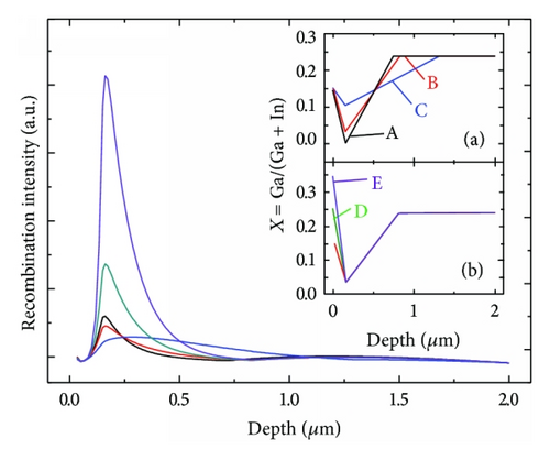
In the varied-notch depth cases, although the recombination intensity is stronger in the deeper notch situation, the ΔEgBack is also increased and provides a higher electric field for carriers to overcome the barrier, hence resulting in lower recombination intensity. In the ΔEgFront cases, larger slope will build up a higher barrier and cause the carriers to be localized in the valley to release energy via radiative recombination. In conclusion, there is an inversely proportional relation between the electric field intensity and recombination intensity. The higher electric field intensity and lower ΔEgFront will cause a lower recombination in the valley. In addition, as the ΔEgBF is positive, the recombination intensity is larger than that of the negative ΔEgBF, which agrees with our speculation. In order to illustrate the observed blocking behavior, the band diagrams of grading profiles are shown in Figure 4.
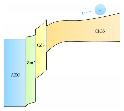
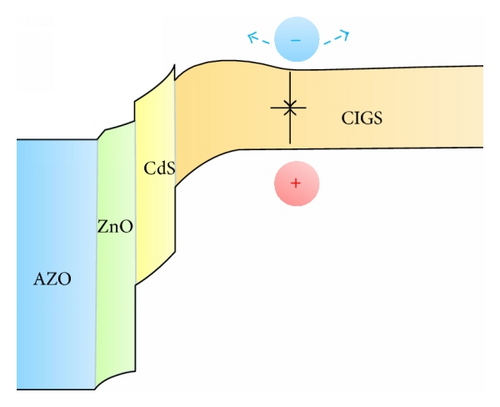
In Figure 4, the diagram describes the influence of ΔEgBF clearly. In the Figure 4(a), the ΔEgBack is larger than ΔEgFront (positive ΔEgBF); ΔEgBack can produce an inner electric field to repel photo-induced electrons reach the backside, thereby reducing the back-surface recombination velocity. However, as Figure 4(b), the ΔEgFront is larger than ΔEgBack (negative ΔEgBF); the inner electric field cannot give enough energy to electrons to reach CdS n-type layer. Therefore, the valley in the conduction band will trap the electrons and lead to an enhanced recombination velocity with the holes in the valence band which reduces the extraction of electricity.
4. Conclusion
In summary, we have developed a well-established model to study the CIGS solar cells with various bandgap absorber layers, and the results are corresponding well to actual device measurements. The simulation results show that a positive ΔEgBF can bring out an inner electric field to reduce back-surface recombination velocity and overcome the front barrier built up by ΔEgFront. On the contrary, the negative ΔEgBF will generate a barrier between CdS and CIGS layer, and the minority carriers (electrons) will be trapped in the valley easier and lead to low device conversion efficiency. In the future, this model can be adopted to optimize the bandgap grading type and fabricate high conversion efficiency CIGS-based thin film solar cell.
Conflict of Interests
The authors declare that there is no conflict of interests regarding the publication of this paper.
Acknowledgments
This work was supported by the Green Technology Research Center of Chang Gung University and the National Science Council (NSC) of Taiwan under contract nos. NSC100-2815-C-155-013-E, NSC100-2112-M-182-004, and NSC101-2112-M-182-003-MY3.


