Optical, Electrical and Photocatalytic Properties of the Ternary Semiconductors ZnxCd1−xS, CuxCd1−xS and CuxZn1−xS
Abstract
The effects of vacuum annealing at different temperatures on the optical, electrical and photocatalytic properties of polycrystalline and amorphous thin films of the ternary semiconductor alloys ZnxCd1−xS, CuxCd1−xS and CuxZn1−xS were investigated in stacks of binary semiconductors obtained by chemical bath deposition. The electrical properties were measured at room temperature using a four-contact probe in the Van der Pauw configuration. The energy band gap of the films varied from 2.30 to 2.85 eV. The photocatalytic activity of the semiconductor thin films was evaluated by the degradation of an aqueous methylene blue solution. The thin film of ZnxCd1−xS annealed under vacuum at 300°C exhibited the highest photocatalytic activity.
1. Introduction
Current materials science requires the creation of new, simple, and low-cost ternary and quaternary semiconductor materials with controllable chemical and physical properties. The chalcogenides have received attention for their ability to relatively easily form binary, ternary, and quaternary compounds. The physical and chemical properties of these compounds principally depend on their compositions.
The chalcogenides have many applications, including photodetectors, photovoltaic devices, optical coatings, electro-optic modulators, field-effect transistors, sensors, transducers, light sources and lasers, and photophysical and photocatalytic applications [1–16]. Ternary and quaternary compounds can easily be obtained from solid-state reactions of bilayers of binary chalcogenides because of the unique physical and chemical properties of these species, including the ionic radii of Cd2+, Zn2+, Cu2+, and Cu1+, which are 103, 83, 72, and 96 pm, respectively [17]. Additionally, wide solubility ranges can be expected for zinc and copper ions in CdS and CuS in films of ternary ZnxCd1−xS, CuxCd1−xS, and CuxZn1−xS compounds. Zn and Cu ions can fill substitutional or interstitial sites in the lattices of CdS and CuS [18].
2. Experimental Methods
2.1. CdS Thin Films
CdS thin films were grown on Corning glass slides by chemical bath deposition (CBD) at a temperature of 90 ± 1°C, over a deposition time of 40 min. The samples were prepared by immersing the substrates vertically in an aqueous solution. The reagents used to prepare the films were cadmium acetate [Cd(CH3COO)22H2O], ammonium acetate (CH3COONH4), ammonium hydroxide (NH4OH), and thiourea [(NH2)2CS]. Cadmium acetate and thiourea served as the sources of Cd and S, respectively. The other components formed complexes in the reaction process and maintained a pH of 9. Highly pure water (≈18 MΩ) was used in the preparation of all of the solutions. The temperature was maintained at 90 ± 1°C with a hot plate equipped with a magnetic stirrer. After being grown, the thin films were rinsed in highly pure water under ultrasonication for 10 min. The average thickness of the films was 80 ± 10 nm [19].
2.2. CuS Thin Films
CuS thin films were grown on CdS/Corning glass substrates by the CBD technique at 40 ± 1°C, over a deposition time of 60 min. The glass slides were immersed vertically in an aqueous solution of copper sulfate (CuSO4·5H2O), sodium acetate (NaCOOH), triethanolamine (HOCH2CH2)3N, and thiourea (CH4N2S). The [Cu]/[S] ratio was 1.5. Highly pure water (≈18 MΩ) was used in the solutions. The temperature was controlled with a hot plate equipped with a magnetic stirrer. Copper sulfate and thiourea served as the sources of copper and sulfur, respectively. After being grown, the thin films were rinsed in highly pure water under ultrasonication for 10 min [20]. The average thickness of the films was 90 ± 10 nm.
2.3. ZnS Thin Films
ZnS thin films were grown on CdS/Corning glass slides by the CBD technique at a temperature of 70 ± 1°C, over a deposition time of 120 min. The samples were prepared by immersing the substrates vertically in the aqueous solution. The reagents used to prepare the films were zinc acetate and thioacetamide. Zinc acetate [(CH3CO2)2Zn] and thioacetamide (CH3CSNH2) served as the sources of Zn and S, respectively. Highly pure water (≈18 MΩ) was used in the preparation of all of the solutions. The temperature was maintained at 70 ± 1°C with a hot plate equipped with a magnetic stirrer. After being grown, the thin films were rinsed in highly pure water under ultrasonication for 10 min. The average thickness of the films was 75 ± 10 nm.
Stacked bilayers of ZnS/CdS/glass, CuS/ZnS/glass, and CuS/CdS/glass were fabricated to obtain ternary compounds. After the growth of the second layer with different thicknesses, they were immediately thermally annealed at different temperatures ranging from 100 to 450°C under vacuum.
The ultraviolet-visible (UV-Vis) spectra of the films were measured on a Perkin-Elmer Lambda-2 spectrophotometer with an uncoated glass substrate placed in the reference beam. The atomic concentrations of the various elements composing the films were measured by electron dispersion spectroscopy (EDS) using a Philips XL30-ESEM. XRD measurements were performed with a RIGAKU Ultima IV using Cu-Kα radiation (λ = 1.54 Å). The films thicknesses were measured on a Sloan Dektak IIA. The resistivity of the films was characterized at ambient temperature using a Loresta-GP instrument.
A photocatalytic activity test was performed with 3.5 mL of an aqueous solution of methylene blue (MB) at a concentration of 2 × 10⁻⁵ mol/L and the ternary thin films were placed in a quartz cell with dimensions of 1 cm × 1 cm × 4 cm and irradiated with a commercial germicidal lamp (λ = 252 nm, 11 W). A rectangular sample with an area of 2 cm2 was inserted into the interior of the quartz cell. The reaction vessel was fixed at a distance of 4.5 cm from the irradiation lamp. The irradiation times were 1 to 5 h, applied in 1-h step. The residual concentration was quantified by UV-Vis absorption spectroscopy at 663 nm. The spectrophotometer was previously calibrated with external calibration standards (2, 1.5, 1.0, 0.5, and 0.25 × 10⁻⁵ mol/L).
3. Results and Discussion
Figure 1 shows SEM images of the ternary semiconductor compounds ZnxCd1−xS, CuxCd1−xS, and CuxZn1−xS annealed under vacuum at 250°C and 450°C. All films covered the substrate surface and were free of pinholes. For films of the semiconductor compound ZnxCd1−xS annealed at 250°C, the superficial morphology was composed of agglomerates approximately 160 nm in diameter with a well-defined spherical shape (Figure 1(a)). The spheres contained small particles measuring 8.5 nm. The spherical shapes of the agglomerates were lost in films annealed at 450°C and nanocracks are evident on the surface of these films. The CuxCd1−xS thin films annealed at 250°C were composed of irregular agglomerates with approximately circular, asymmetric shapes, and a distribution of sizes and both small particles (Figure 1(c)) and nanocracks were evident. At an annealing temperature of 450°C, the agglomerates exhibited better-defined shapes and stacking faults (Figure 1(d)). The thin films of the ZnxCu1−xS semiconductor demonstrated a superficially amorphous nature (Figures 1(e) and 1(f)).

Table 1 shows the EDS analysis results of the three ternary compounds at the vacuum annealing temperatures of 250 and 450°C. The compounds containing cadmium are generally rich in cadmium at low temperature (250°C); however, at high temperature, where diffusion is favored, the cadmium concentration diminishes and, consequently, the respective concentrations of zinc and copper increase (ZnxCd1−xS and CuxCd1−xS). The compound CuxZn1−xS is rich in zinc at low temperature. The copper concentration increases at high temperature.
| Sample | TAnn/(°C) | Zn (at. %) | Compound |
|---|---|---|---|
| ZnxCd1−xS | 250 | 29.43 | Zn0.3Cd0.7S |
| 450 | 44.84 | Zn0.45Cd0.55S | |
| Cu (at. %) | |||
| CuxCd1−xS | 250 | 11.24 | Cu0.11Cd0.89S |
| 450 | 18.03 | Cu0.18Cd0.82S | |
| CuxZn1−xS | Cu (at. %) | ||
| 250 | 28.59 | Cu0.29Zn0.71S | |
| 450 | 34.6 | Cu0.35Zn0.65S | |
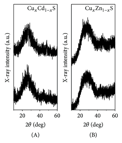
Figures 2(a) and 2(b) display the XRD results obtained over a 2θ range of 15 to 60 degrees for the ternary semiconductor alloys CuxCd1−xS, CuxZn1−xS, and ZnxCd1−xS annealed under vacuum. For Figure 2(a) in all cases, the thin films were amorphous independent of the annealing temperature. At 250°C, the samples were most amorphous, and at 450°C, small peaks appeared. Figure 2(a) (A) shows the XRD results obtained for thin films of CuxCd1−xS, the patterns show two peaks at 44.28° and 52.44° and at 43.04° and 47.8° for films annealed under vacuum at 250°C and 450°C, respectively. Figure 2(a) (B) shows the XRD results obtained for nanocrystalline thin films of CuxZn1−xS, which indicate a single one peak at 43.26° and 45.16° for films annealed under vacuum at 250°C and 450°C, respectively. The small peaks made it difficult to identify the phase.
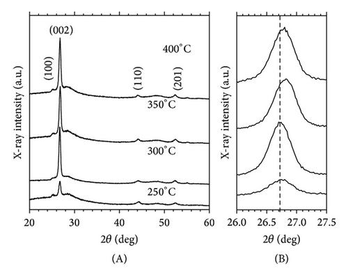
As shown in Figure 2(b) (A), at 250–450°C ZnxCd1−xS shows peaks at 25.13°, 26.8°, 44.2°, and 52.4°, corresponding to the hexagonal wurtzite planes of (100), (002), (110), and (201) in thin films of the standard PDF Card 00-049-1302. Figure 2(b) (B) shows that the orientation of the films is in the plane (002), with the increase of annealing temperature, these peaks move to higher diffraction angle, indicative of an increase of Zn content in the films. The grains size was calculated from Scherrer’s equation for the peaks (002) as a function of the annealing temperature and varied for 16.316 nm, 19.95 nm, 19.43 nm, and 19.50 nm, respectively, for 250, 300, 350, and 400°C.
Figures 3(a), 3(b), and 3(c), respectively, show the UV-Vis transmission spectra as a function of annealing temperature for ZnxCd1−xS, CuxCd1−xS, and CuxZn1−xS films annealed under vacuum. The ZnxCd1−xS films exhibited high transmittances > 80% over an annealing temperature range of 250°C to 450°C. For the CuxCd1−xS thin films, the transmittance was approximately 65%; higher transmittance was observed for the films annealed under vacuum at 300°C than for those annealed at 250°C. The CuxZn1−xS thin films showed the lowest transmittance values of 35 to 50%; the highest transmittance was observed for the films annealed at 350°C and the lowest for those annealed at 300°C. The optical band gap, Eg, of each film was calculated using the Tauc equation by plotting (αhν)2 as a function of hν, where α is the optical absorption coefficient and hν is the photon energy. In the graphs, the linear portion of the curve was extrapolated to (αhν)2 = 0. The band gap is shown as a function of the annealing temperature in Figure 4. For ZnxCd1−xS, the Eg values decreased from 2.83 to 2.5 eV as a function of the vacuum annealing temperature. For the CuxCd1−xS thin films, the Eg values decreased from 2.43 to 2.28 eV by increasing the annealing temperature. The ZnxCu1−xS thin films showed Eg values of 2.80 to 2.65 eV, with the increase of the annealing temperature. The Eg values are in agreement with the values reported by other research groups [21–23]. In general, the band gap decreases as the annealing temperature increases; this effect may be caused by both the greater diffusion between the bilayers and the formation of the ternary alloy.
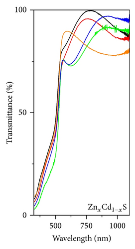
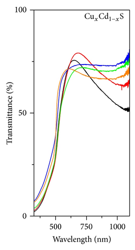
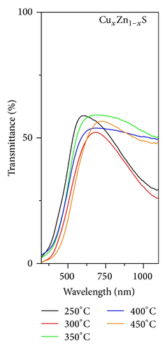
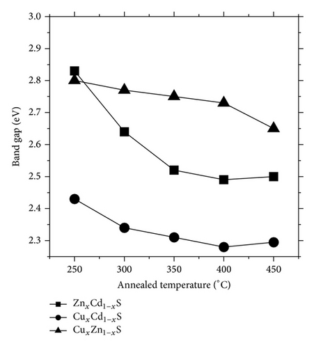
Figure 5 shows the resistivity values of the ternary semiconductor compounds. The thin films of ZnxCd1−xS were highly resistive independent of thermal annealing; the resistivity values were greater than 106 Ω·cm (results not shown). Figure 5 displays the resistivity values of the CuxCd1−xS and CuxZn1−xS films annealed under vacuum as a function of the annealing temperature. The values for CuxCd1−xS decreased as the annealing temperature increased. The minimum resistivity occurred at 300°C (2.74 × 10⁻³ Ω·cm), above this temperature, the resistivity value increased. The resistivity values for the CuxZn1−xS samples decreased as the annealing temperature increased. The lowest value was obtained at 350°C (4.11 × 10⁻⁴ Ω·cm) and, for temperatures above 350°C, the resistivity values increased.
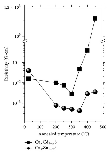
The change of resistivity values with the change of the annealing temperatures could be attributed to the diffusion of copper ions on the matrix of CdS and ZnS, with the temperature increase and the presence of nanocracks on the surface of the films at elevated temperatures. The ionic radii of Cd2+, Zn2+, and Cu2+, are 103, 83, and 72 pm, respectively [17], on the other hand, the copper ions could be introduced more effectively with the increase of the temperature until the saturation, and possibly the segregation phenomena takes place at different temperatures (300 and 350°C for CuxCd1−xS and CuxZn1−xS, resp.). Copper ions are closer to the ionic radii of Zn2+ than Cd2+. Additionally, copper ions could be introduced more easily in the ZnS lattice occupied substitutional or interstitial sites in the lattices of ZnS than in CdS [18].
To demonstrate the prospective photocatalytic applications of the fabricated materials, the thin films were used as catalysts in the degradation of methylene blue (MB) under germicidal irradiation (λ = 252 nm) at room temperature. Figure 6 displays the normalized concentration of MB in aqueous solution as a function of the vacuum annealing temperature for the three different semiconductor alloys. The concentration was quantified based on the absorption at 653 nm.
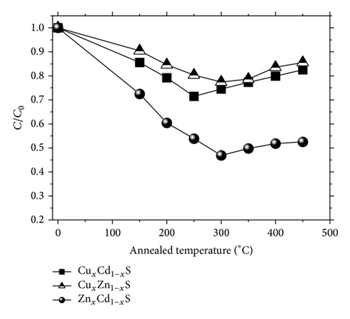
The absorption is time-dependent, initially, the irradiation time was held constant at 3 h for all samples. The ternary semiconductor samples generally showed photocatalytic behavior. The sample with the best photobleaching performance was ZnxCd1−xS annealed at 300°C (see Figure 6).
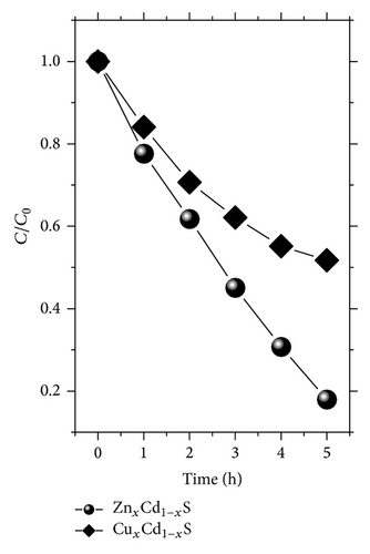
As indicated in Figure 6, the best samples were ZnxCd1−xS and CuxCd1−xS annealed at 300°C and 250°C, respectively. The temporal dependence of the photobleaching of MB by these samples was analyzed. Figure 7(a) shows the normalized MB concentration as a function of time in hours. The ZnxCd1−xS film demonstrated that it is an excellent candidate for photocatalytic applications. In 5 h, the mineralization of MB was nearly complete (82%) for the thin films of ZnxCd1−xS annealed under vacuum at 300°C. This can be attributed to the synergistic effect of thermal annealing, better crystallinity, and concentration of the Zn mole fraction to 0.3 and 0.33 for 250 and 300°C, respectively; similar results were found by an optimal Zn incorporation corresponding to x approximately 0.2–0.33 [24–27]. Additionally these results are comparable to the photocatalytic activities reported in the literature for thin films of other materials, such as ZnO and TiO2, which have been shown to be excellent catalyzers [28–31].
The thin films of ZnxCd1−xS were obtained by chemical bath deposition and were annealed under vacuum at 300°C. Obtaining this film is very economical compared to the preparation of films of ZnO (sol-gel, sputtering at T ≥ 500°C) and TiO2 (sol-gel, sputtering at T ≥ 450°C). Additionally, our films have high transmittances (≥85%) and band gaps (2.5 to 2.83 eV) closer to the absorption spectrum of visible light than gaps larger than 3.2 eV (ZnO and TiO2).
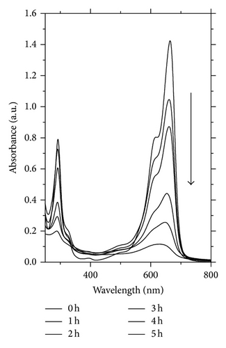
For CuxCd1−xS annealed at 250°C, the extent of mineralization after 5 h was approximately 50%. Figure 7(b) displays the absorption spectra of an aqueous solution of MB at different intervals in the presence of a sample of ZnxCd1−xS annealed at 300°C. The concentration was quantified based on the absorption at 653 nm. The absorption was time-dependent and the complete mineralization of MB was nearly reached after 5 h under the experimental conditions described above.
4. Conclusions
Simple and economical syntheses of ternary semiconductor alloys of ZnxCd1−xS, CuxCd1−xS, and CuxZn1−xS were obtained by the chemical bath deposition and subsequent annealing of stacked bilayers of binary semiconductor films. The three compounds showed good optical properties, superficial morphology, and photocatalytic activity. The band gap of the CuxCd1−xS and CuxZn1−xS samples was tuned from 2.3 to 2.85 eV. These samples demonstrated the lowest resistivity values of 2.74 × 10⁻³ and 4.11 × 10⁻⁴ Ω·cm, respectively, among all of the films that were fabricated. Extensive photodegradation of methylene blue was observed for the ZnxCd1−xS film annealed at 300°C in vacuum; this activity is comparable to that reported in the literature for thin films of ZnO and TiO2.
Conflict of Interests
The authors declare that there is no conflict of interests regarding the publication of this paper.
Acknowledgments
The authors thank the Universidad Autónoma de Querétaro México for the financial support of this work through the Project FOFI 2012 and the CONACYT Projects CB154787 and CB176450.


