Performances of an Interleaved High Step-Up Converter with Different Soft-Switching Snubbers for PV Energy Conversion Applications
Abstract
This paper proposes an interleaved high step-up converter with different soft-switching snubbers for PV energy conversion applications. For the high step-up converter, interleaved and coupled-inductor technologies are used to reduce output ripple current and increase output power level. Simultaneously, two types of snubbers, a single-capacitor snubber and boost type snubber, are introduced separately into the discussed converters for comparing their performances of conversion efficiency and switching losses. For drawing maximum power from the PV arrays, a perturbation-and-observation method realized with the microcontroller is adopted to achieve maximum power point tracking (MPPT) algorithm and power regulating scheme. Finally, two prototypes of the interleaved coupled-inductor boost converter with a single-capacitor snubber and with boost type snubber are implemented, respectively. The experimental results obtained are used to verify and compare the performances and feasibilities of the discussed converters with different snubbers in PV conversion applications. The experimental results show that the proposed system is suitable for PV energy conversion applications when the duty ratios of switches of the converter are less than 0.5.
1. Introduction
In recent years, in order to offer enough energy to maintain the economic development of the world, one of the solutions is the solar energy which is a totally inexhaustible and completely clear energy source. However, due to the instability and intermittent characteristics of solar energy, photovoltaic (PV) power conversion systems with power converter and maximum power tracking algorithms are needed to convert solar energy into electrical energy and provide stable power output. With the rapid growth of power electronics techniques, the conversion efficiency of PV power conversion system has been increased obviously [1, 2]. Recently, PV power conversion systems are well recognized and widely used in electric power conversion system, such as PV power generation for grid connection, PV vehicle constriction, battery charger, water pumping, and satellite power conversion system.
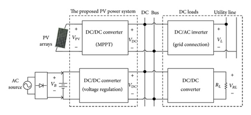
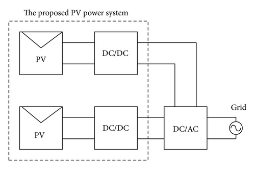
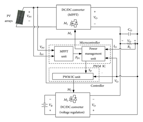
To extract power from PV arrays, power converter is used in PV power conversion systems. In order to obtain the maximum power from PV arrays and thus increase utility rate of PV arrays, switching-mode converter must be operated at the maximum power point (MPP) of PV arrays, resulting in its output voltage without keeping in the desired dc constant voltage. Therefore, a switching-mode one with battery source in parallel is used for keeping the output voltage in the desired dc constant voltage, as shown in Figure 1(a). In Figure 1(a), dc voltages provided by the proposed PV power conversion system can be supplied to dc loads of dc/ac inverters for grid-connected power conversion system [3–8] and dc/dc converter for dc load [9–13]. In grid-connected power conversion system applications, control of power converters has to be taken into consideration. In [4], three different control topologies have been proposed according to the number of power processing stages. Since the multistage topology, as shown in Figure 1(b), possesses a better control performance of each DC/DC converter, it is adopted in the proposed PV power conversion system. Therefore, the PV power conversion system consists of a switching-mode converter for maximum power point tracking (MPPT) of PV arrays and a switching-mode converter for voltage regulation of dc load under the control of multistage topology.
In the MPPT algorithm research, several MPPT algorithms have been proposed [14–23]. Some of the popular MPPT algorithms are constant voltage method [14, 15], system oscillation method [16, 17], ripple correlation method [18], β method [19], incremental conductance method [20], and perturbation-and-observation method [21–23]. Under the consideration of simplicity and easy implementation, the perturbation-and-observation method is adopted and used in the proposed PV power conversion system.
For PV arrays, since output voltage VPV of the PV arrays is in a low voltage level, the DC/DC converter with a higher step-up voltage ratio is needed [24–28]. In [24], the voltage-fed converters are not the optimal candidates for high step-up applications because they usually have a buck type configuration and (or) LC filter in the secondary rectification circuits. With this circuit structure, it results in a large transformer turns ratio, which makes the transformer design complex and leads to a large leakage inductance. Compared with the voltage-fed converters, the current-fed converters [25–27] and the coupled-inductor converters [28] are preferable choices for high voltage conversion ratio applications. Although the current-fed converters are adopted in the PV power system, they are also used as a voltage doubler or multiplier to increase the step-up voltage ratio. When the converters adopt the voltage doubler or multiplier, capacitors of the voltage doubler must be special capacitors with a low equivalent series resistance (ESR), high current ripple rating (CRR), and high operational bandwidth. Therefore, it is only suitable for using in the low power level applications. In [28], a high step-up converter achieved by a coupled inductor is presented. Compared with converters using an isolation transformer to obtain the high step-up voltage ratio, the one using the coupled inductor has a more simple winding structure and higher coupling coefficient. It not only reduces inductor currents to ensure a lower conduction loss but also decreases leakage inductance to attain a lower switching loss. Therefore, the boost converter with the coupled inductor is used in the proposed system.
For further increasing the power capability of the converter, the boost converter used in the proposed system is constructed in an interleaved manner [29–33]. Moreover, PWM ICs with two gate signals are used to drive switches of the interleaved converter. Since the voltage fed type of input sources are used in the converters and it is difficult to obtain a special PWM IC with duty ratio greater than 0.5 (≥0.5), PWM ICs with duty ratio within 0.5 are used to control the switches in the discussed boost converters. Therefore, the operation of the proposed converter is constrained under duty ratio of 0.5.
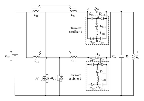
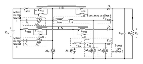
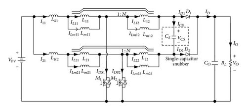
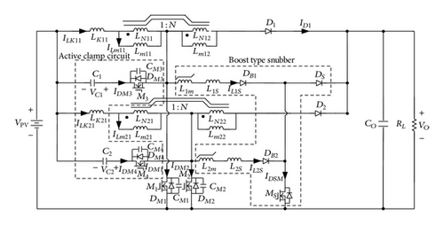
When a coupled inductor boost converter is used in the PV power conversion system, the energy trapped in the leakage inductor of coupled inductor not only increases voltage stresses but also induces switching lossless of switches in the converter, significantly. In order to solve these problems, several methods have been proposed [34–36]. In [34], a resistor-capacitor-diode (R-C-D) snubber is used to alleviate voltage stresses of switches by dissipating the energy trapped in the leakage inductor through the resistor, reducing the conversion efficiency of the converter. Therefore, a passive lossless circuit proposed in [35] is adopted to reduce voltage spike across switches. Its schematic diagram with the interleaved manner is shown in Figure 2. Although converters with a passive lossless circuit can improve conversion efficiency, active switches are still operated in hard switching at turn-on transition. In [36], an active clamp circuit is introduced to achieve zero-voltage switching (ZVS) and increased its conversion efficiency. However, the disadvantage of the active clamp circuit is that it is difficult to implement soft-switching features at light load for the boost converter. In order to solve this problem, a boost type snubber is inserted into the active clamp boost converter with coupled inductor, as shown in Figure 3. It can improve conversion efficiency of the boost converter at light load, significantly. Due to the complexity of circuit structures shown in Figures 2 and 3, they are, respectively, simplified by [37] and [38] and are shown in Figures 4(a) and 4(b). In this paper, performance comparisons between the discussed converters with the single-capacitor snubber and with boost type snubber are proposed.
2. Control Algorithm of the Proposed Converter
When a switching-mode dc/dc converter is adopted as their power processor for extracting power from PV arrays and converting the power into dc voltage supplied to dc loads, a proper power management system for managing the power is needed in the PV power conversion system. In the following, the circuit topology of the proposed converter power conversion system, MPPT algorithm, and power management are described.
2.1. Circuit Topology of the Proposed Converter
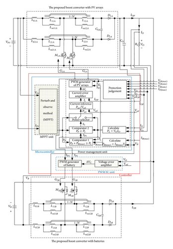
The proposed PV power conversion system uses PV arrays as one of its power sources. For increasing the utility rate of the PV arrays, the PV arrays have to be operated on their maximum power. Therefore, as shown in Figure 5, a PV power conversion system constructed of a switching-mode converter with PV array sources, a switching-mode converter with battery source, and a controller is proposed. In the proposed PV power system, the two dc/dc converters are realized by an interleaved coupled-inductor boost converter with single-capacitor snubber shown in Figure 4(a). The one with PV arrays source uses MPPT control algorithm for extracting the maximum power from PV arrays. The other with battery source uses voltage regulation control method to regulate powers between PV arrays and loads and to generate a constant output voltage supplied to dc loads. As shown in Figure 5, controller constructed by MPPT unit, power management unit, and PWM IC unit is used to control the dc/dc converter with PV array source for determining the MPP of PV arrays by the perturbation-and-observation method described in [21–23]. There are two signals generated by the power management, control signals M1 and SP. Control signal M1 is used to regulate output powers of switching-mode converter with MPPT control algorithm. Control signal SP is generated according to the relationships between the maximum power PPV(max ) of PV arrays and power of load PL. Based on the control signal SP and the output VO, PWM IC unit generates control signal M2 with voltage regulation control method for obtaining constant output voltage. Protections are considered and implemented by microcontroller. The protections include over-current, over-voltage, and over-temperature protections of the two converters and undercharge of battery. Therefore, the proposed PV power conversion system can be used to achieve the optimal utility rate of PV arrays.
2.2. Power Management
The power of PV arrays is supplied to the load through the proposed interleaved boost converter. The power management of the proposed power conversion system is implemented by a microcontroller and is used to regulate the power of PV arrays and output power. According to relationships among the powers of PPV, PVB, and PL, operational modes of power management can be divided into 8 modes and are illustrated in Table 1. Power PPV is output power of switching-mode converter with PV arrays as its power source, PVB is that of switching-mode converter with battery as its power source, and PL is power of load. Moreover, “1” represents that the power is generated by switching-mode converter or is required by load, while “0” represents that the power is not generated by switching-mode converter or is not required by load. According to the operational modes illustrated in Table 1, PV power conversion system is shut down in operational modes of I, II, III, V, and VII. Therefore, operational modes IV, VI, and VIII are described as follows.
| Operational modes | Power states | Operational conditions of PV power conversion system | ||
|---|---|---|---|---|
| PPV | PVB | PL | ||
| I | 0 | 0 | 0 | Shutdown |
| II | 0 | 0 | 1 | Shutdown |
| III | 0 | 1 | 0 | Shutdown |
| IV | 0 | 1 | 1 | Working |
| V | 1 | 0 | 0 | Shutdown |
| VI | 1 | 0 | 1 | Working |
| VII | 1 | 1 | 0 | Shutdown |
| VIII | 1 | 1 | 1 | Working |
2.2.1. Operational Mode IV
In mode IV, the switching-mode converter with battery is used to supply power to the load. Once the condition of PL > PVB(max ) is reached or energy stored in battery is completely discharged, the proposed converter is shut down.
2.2.2. Operational Mode VI
In mode VI, the switching-mode converter with PV arrays as its power source is used to supply power to load. When power of PPV(max ) is equal to or greater than that of PL, power curve of PV arrays follows that of load. Once PPV(max ) < PL, the proposed converter is shut down.
2.2.3. Operational VIII
When PV power conversion system is operated in mode VIII, the interleaved boost converter supplies power to load, as shown in Figure 6. During this operational mode, (PPV(max ) + PB(max )) must be equal to or greater than PL. If (PPV(max ) + PB(max )) < PL, the proposed PV power conversion system is shut down. When (PPV(max ) + PB(max )) ≥ PL, the operational condition can be further divided into two cases: PPV(max ) ≥ PL and PPV(max ) < PL. In the following, the two cases are briefly described.
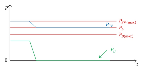
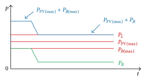
(1) PPV(max ) ≥ PL and PB(max ) < PL. When PPV(max ) ≥ PL and PB(max ) < PL, the switching-mode converter with battery source is shut down, causing the output power PPV of PV arrays to be equal to PL, as shown in Figure 6(a). Hence, the switching-mode converter with PV arrays source is operated in voltage regulation mode to supply the desired dc voltage to load.
(2) PPV(max ) < PL and PB(max ) < PL. When PPV(max ) < PL and PB(max ) < PL, the switching-mode converter with PV array source is operated at the MPP of PV arrays to extract the maximum power from the PV arrays. On the other hand, the one with battery source is used to sustain the desired dc voltage. Power curve for operational mode VIII under PPV(max ) < PL and PB(max ) < PL is shown in Figure 6(b). From Figure 6(b), it can be seen that PL is the sum of PPV and PB.
3. Control Design of the Proposed PV Power Conversion System
As shown in Figure 7, controller of the proposed power conversion system consists of two major units, the microcontroller and the PWM IC units. The microcontroller is further divided into the MPPT unit and the power management unit. In the following, functions of each block will be described briefly.
3.1. The MPPT Unit
The MPPT unit uses the perturbation-and-observation method to track MPPT of PV arrays and to decide the maximum power PPV(max ) of PV array, resulting in the output power of PP for further power management.
3.2. The Power Management Unit
In the power management unit, the maximum discharging current IB(max ) of battery is set for obtaining the maximum battery discharging power PB(max ) of VBIB(max ). Based on the output power of MPPT unit PP, the maximum battery discharging power, and the load power PL of VOIO, comparator number 1 determines the relationships between (PPV + PB(max )) and PL. There are two relationships to be discussed.
3.2.1. Case I: (PPV + PB(max)) ≥ PL
When (PPV + PB(max )) ≥ PL, control signal SP1 of comparator number 1 is in the low level, causing further comparison of PP and PL in comparator number 2. If PP ≥ PL, the low level output signal S1 of comparator number 2 makes the power selector to set the power Pset to be equal to PL. Once PP < PL, output signal S1 of comparator number 2 becomes a high level and causes the power selector to set the power Pset to be equal to PP. Then, in the reference current block, the power Pset and the reference voltage Vref are used to calculate the reference current IC for obtaining the current error value ΔIC (=IC − IOP) with output current of the proposed converter with PV array source, IOP, in the current error amplifier.
In the PWM generator of PV array, control signals G1A and G2A are obtained by comparing current error value ΔIC with triangular wave generated by the PWM generator of PV arrays. The control signals G1A and G2A are used to drive switches M1A and M2A of the proposed converter with PV array source for controlling power flowed from PV arrays to load.
3.2.2. Case II: (PPV + PB(max)) < PL
When (PPV + PB(max )) < PL, control signal SP1 of comparator #1 is in the high level, causing both of PWM generators of PV array and battery to be shut down. The power management unit also includes functions of protection, which are over-voltage, over-current, under-voltage, and undercharge protections. As shown in Figure 7, there are six input signals to the protection controller, VO(max ), VO(min ), IO(max ), VB(max ), IO, VO, and VB, where VO(max ) and VO(min ) are maximum and minimum values of output voltage, IO(max ) is maximum value of output current, VB(min ) is minimum value of battery voltage, IO is output current, VO is output voltage, and VB is voltage of battery. When VO ≥ VO(max ), the proposed converter is operated in over-voltage condition, causing the output signal SP2 to be in a high level and shut down both of the PWM generators. Moreover, conditions of IO ≥ IO(max ) (over-current condition), VO ≤ VO(min ) (under-voltage condition), or VB ≤ VB(min ) (undercharge condition) also make signal SP2 to be in a high level to shut down both of the PWM generators.
3.3. The PWM IC Unit
The proposed boost converter with battery source uses lead-acid battery as its power source. In order to implement power balance among PV arrays, battery, and load and sustain a constant output voltage, a PWM IC unit is adopted. This control unit includes voltage error amplifier and PWM generator of battery. Based on the output voltage VO and reference voltage Vref, the voltage error amplifier determines the voltage error value ΔVC of (Vref − VO). The voltage error value ΔVC is then sent to PWM generator of battery to be compared with triangle wave generated by PWM IC for obtaining PWM signals G1B and G2B. Signals G1B and G2B are used to control switches M1B and M2B for regulating powers between PV arrays and load. Similarly, the PWM generator of battery can be shut down either by signals SP1 or SP2.
4. Experimental Results
- (A)
The proposed boost converter with PV arrays is as follows.
- (i)
Input voltage VPV: 34~42 V (PV arrays).
- (ii)
Output voltage VO: 400 Vdc.
- (iii)
Output maximum current IOP(max ): 3 A.
- (iv)
Output maximum power PPV(max ): 1.2 kW.
- (i)
- (B)
The proposed boost converter with battery is as follows.
- (i)
Input voltage VB: 44~54 Vdc (4 sets of 12 V battery connected in series).
- (ii)
Output voltage VO: 400 Vdc.
- (iii)
Output maximum current IOB(max ): 3 A.
- (iv)
Output maximum power PB(max ): 1.2 kW.
- (i)
- (i)
Switches M1A, M2A, M1B, and M2B: IRFP260N.
- (ii)
Diodes D1A, D2A, D1B, and D2B: HFA08TB120 × 2 (connected in series).
- (iii)
Coupled inductors Lm11, Lm21: 30 μH.
- (iv)
Leakage inductors of coupled inductors (Lm11, Lm12) and (Lm21, Lm22): 1.1 μH.
- (v)
Cores of coupled inductors (Lm11, Lm12) and (Lm21, Lm22): EE-55.
- (vi)
Turns ratio N: 20.
- (i)
Switches M1A ~ MSA: IRFP260N.
- (ii)
Switches M1B ~ MSB: IRFP260N.
- (iii)
Diodes D1A, D2A, D1B, and D2B: HFA08TB120 × 2 (connected in series).
- (iv)
Diodes DB1A, DB2A, DB1B, DB2B, and Ds: HFA08TB120 × 2 (connected in series).
- (v)
Coupled inductors Lm11, Lm21: 30 μH.
- (vi)
Leakage inductors of coupled inductors (Lm11, Lm12) and (Lm21, Lm22): 1.1 μH.
- (vii)
Cores of coupled inductor (Lm11, Lm12) and (Lm21, Lm22): EE-55.
- (viii)
Turns ratio N: 20.
- (ix)
Inductors L1s, L2s: 3 μH.
- (x)
Cores of inductors L1s, L2s: DR28X12.
- (xi)
Capacitors C1A, C2A, C1B, C2B: 15 μF.
To verify performances of the high step-up converter applied to the PV power system, some of important comparisons have been made and listed in Table 2. It can be seen from Table 2 that the proposed boost converter with the single-capacitor snubber has less component counts, lower cost, and easier control circuit, while the proposed one with boost type snubber has more component counts, higher cost, more complexity control circuit, and high conversion efficiency. They are suitable for middle or high power level applications. In addition, although the high step-up converters proposed in [25, 27] have higher conversion efficiency, they are only applied to low or middle power level applications.
| Items for comparison | The proposed boost converter with single-capacitor snubber | The proposed boost converter with boost type snubber | The boost converter proposed in [25] | The high step-up converter proposed in [27] |
|---|---|---|---|---|
| Key component counts | ||||
| Active switch | 2 | 5 | 4 | 4 |
| Passive switch | 2 | 5 | 4 | 2 |
| Magnetic core | 2 | 6 | 4 | 3 |
| Resonant/output capacitor | 2 | 3 | 6 | 3 |
| Seft-switching features | ||||
| Main switches |
|
|
|
|
| Auxiliary switches |
|
|
|
|
| Cost | Lower | High | Middle | Low |
| Duty ratio limitation | D < 0.5 | D < 0.5 | D > 0.5 | D > 0.5 |
| Turns ratio of transformer | 20 | 20 | 2.5 | 2.125 |
| Control complexity | Middle (86%) | High (90%) | Higher (94.4%) | Highest (96%) |
| Conversion efficiency under full load condition | Simplicity | Complexity | Complexity | Complexity |
| Power level application | Middle power level | High power level | Lower power level | Low power level |
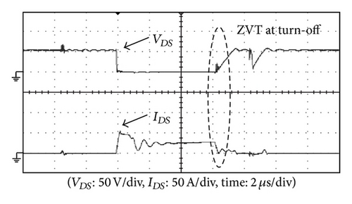
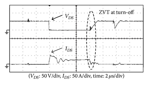
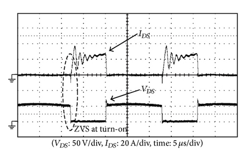
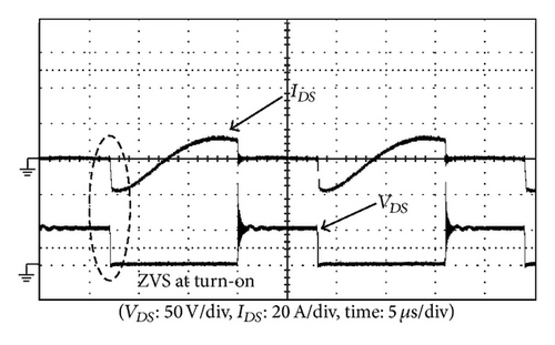
Moreover, hardware dimension of each DC/DC converter is about 210 × 297 mm. In order to verify the feasibility of the proposed boost converter with battery source, measured voltage VDS and current IDS waveforms of switches are shown in Figures 8 and 9. Figure 8 shows those waveforms of switches M1B and M2B under 50% of full-load condition when the proposed one adopts the single-capacitor snubber, while Figure 9 shows those waveforms of switches M1B and M3B under 20% of full load condition when the proposed one uses boost type snubber. Experimental results reveal that when the discussed boost converter with the single-capacitor snubber is adopted, switches can be operated with zero-switching transition (ZVT) at turn-off transition. Switches of the discussed one with boost type snubber are operated with ZVS at turn-on transition.
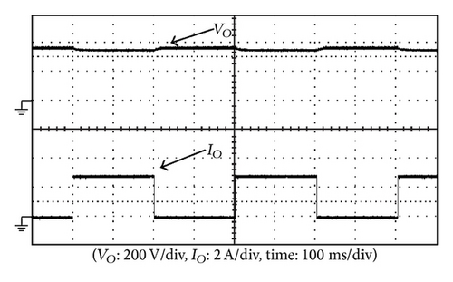
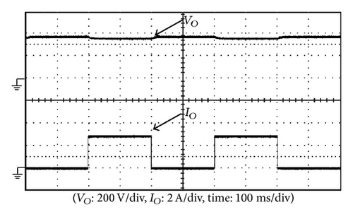
To make a fair comparison, the components of the boost converter with hard-switching circuit, the single-capacitor snubber, and boost type snubber are kept the same as possible. Figure 10 shows measured output voltage VO and current IO waveforms of the boost converter with three different snubbers under step-load changes between 0% and 100% of full load with repetitive rate of 0.5 Hz and a duty ratio of 50%. From Figure 10, it can be observed that voltage regulations of output voltage VO of boost converter with the single-capacitor snubber and boost type snubber are approximately the same as the one with hard-switching circuit. It reveals that the boost converter with the single-capacitor snubber and boost type snubber can yield a good dynamic performance.
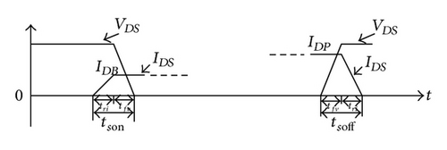
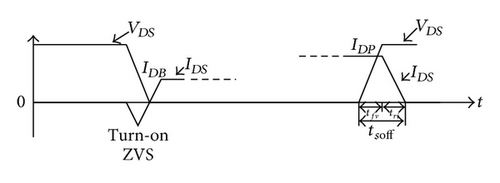
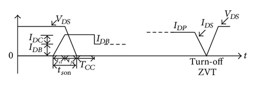
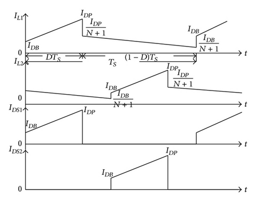
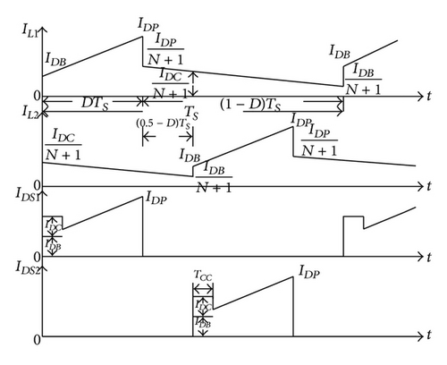
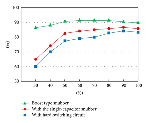
According to the operational principles of the proposed converters with the single-capacitor snubber and the boost type snubber, switches of the proposed one with the single-capacitor snubber have ZVT features at turn-off transition, while those switches with the boost type snubber have ZVS features at turn-on transition. Their conceptual waveforms are illustrated in Figures 11(b) and 11(c), respectively. Figures 12(a) and 12(b) show the current waveforms of switches and inductors in the interleaved coupled-inductor boost converter with hard-switching circuit and the single-capacitor snubber, respectively. From Figure 12(b), it can be seen that when switch of one boost converter in the interleaved boost converter is turned on, the diode current IDC of the other boost converter in the interleaved one flows through the switch by the capacitor snubber. Therefore, the boost converter with the single-capacitor snubber will induce an extra turn-on switching loss. The key parameter values of the proposed interleaved boost converters with the single-capacitor snubber and with the boost type snubber under full-load condition are listed in Tables 3 and 4, respectively. It can be found from Tables 3 and 4 that switching losses of the proposed converter with the single-capacitor snubber, compared with those of the proposed one with the boost type sunbber, increase by 20~30 W. Comparison of efficiencies among the discussed interleaved boost converters with different types of snubbers is illustrated in Figure 13. It shows that the boost converter with boost type snubber can yield the highest conversion efficiency than that with single-capacitor snubber from light load to heavy load. Conversion efficiencies of boost converters under full-load condition with boost type snubber and single-capacitor are 86% and 90%, respectively. Since duty ratios of switches in two discussed PV power conversion systems are less than 0.5, their turns ratios of coupled inductors have higher values. Therefore, a higher current flows through switches of the converter, resulting in a larger switching losses and conduction losses. Therefore, conversion efficiency of the converter in the two discussed PV power conversion systems can be further increased by reducing turns ratio of coupled inductor. Moreover, if the conducted resistances RDS(on ) of switches in the converters are reduced, those in the two discussed PV power conversion systems will be increased. That is, a lower conducted resistance RDS(on ) of switch can be chosen. In addition, two switches connected in parallel can be used for reducing the conducted resistance. By doing so, conversion efficiency of the proposed converter can be further increased by about 3~5%.
| Parameters | Formulas | Calculation values | Practical values |
|---|---|---|---|
| IDB | 38.87 A | 39.5 A | |
| IDP | 54.47 A | 56 A | |
| IDC | 12 A | 63 A | |
| Switch stress VDS(max ) | 53 V | 55 V | |
| Voltage across snubber capacitor VCS | (VO + NVPV) | 1120 V | 1120 V |
| Output diode stress | (VO + NVPV) | 1120 V | 1500 V |
| Duty ratio D | 0.325 | 0.34 | |
| Snubber capacitor CS | 1.16 nF | 10 nF | |
| TCC | 1.2 ns | 9.9 ns | |
| Switching loss of each switch at turn-on Pson | 5.86 W | 21.14 W | |
| Switching loss of each switch at turn-off Psoff | 0 W | 0 W | |
| Conduction loss of each switch PSC | 28.58 W | 30.31 W | |
| Conduction loss of diode PSCD | 7.2 W | 7.5 W | |
| Forward drop voltage VDF of output diode |
|
|
|
| tson | 87 ns | 150 ns | |
| tsoff |
|
|
|
| VPV | 36 V | 36 V | |
| VO | 400 V | 400 V | |
| TS | 20 μs | 20 μs | |
| IO | 3 A | 3 A | |
| N | 20 | 20 | |
| ton | DTS | 6.5 μs | 6.8 μs |
| Rds | 0.04 Ω | 0.04 Ω |
| Parameters | Formulas | Calculation values | Practical values |
|---|---|---|---|
| IDB | 38.87 A | 39 A | |
| IDP | 54.47 A | 56 A | |
| Switch stress VDS(max ) | 53 V | 55 V | |
| Output diode stress | (VO + NVPV) | 1120 V | 1500 V |
| Duty ratio D | 0.325 | 0.34 | |
| Switching loss of each switch at turn-on Pson | 0 W | 0 W | |
| Switching loss of each switch at turn-off Psoff | 7.43 W | 9.24 W | |
| Conduction loss of each switch PSC | 28.58 W | 30.31 W | |
| Conduction loss of diode PSCD | 7.2 W | 7.5 W | |
| Forward drop voltage VDF of output diode | 4.8 V (2.4 × 2) | 4.8 V | |
| tson | 87 ns | 100 ns | |
| tsoff | 103 ns | 120 ns | |
| VPV | 36 V | 36 V | |
| VO | 400 V | 400 V | |
| TS | 20 μs | 20 μs | |
| IO | 3 A | 3 A | |
| N | 20 | 20 | |
| ton | DTS | 6.5 μs | 6.8 μs |
| Rds | 0.04 Ω | 0.04 Ω |
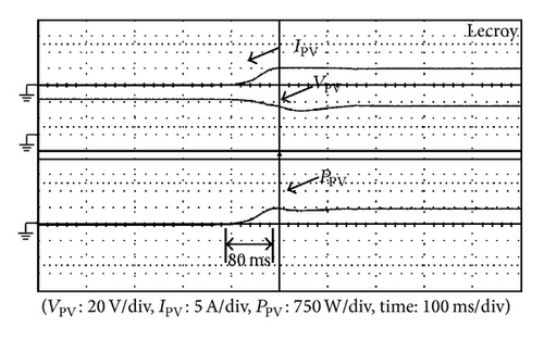
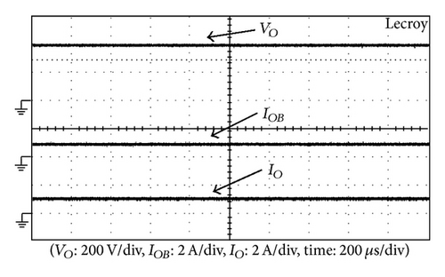
Since the proposed boost converters with the single-capacitor and boost type snubbers use the same control method, the measured results for MPPT and power management should be the same. Therefore, only the measured results of the proposed one with the single-capacitor snubber are shown in this paper. From the measured waveforms of voltage VPV, current IPV, and power PPV under PPV(max ) = 750 W shown in Figure 14, the tracking time of MPPT realized by the proposed converter with PV arrays as its power source is about 80 ms from 0 to the maximum power of PV arrays. Figure 15 shows the measured waveforms of output voltage VO and current IOB and IO under PL = 350 W, as the power management of the proposed PV power conversion system is operated in mode IV and PB(max ) ≥ PL. From Figure 15, it can be seen that output voltages VO are sustained at 400 V and current IBO is equal to IO. When the proposed PV power conversion system with the single-capacitor snubber is operated in mode VI and PPV(max ) ≥ PL, measured waveforms of output voltage VO and currents IOP and IL under PPV(max ) = 700 W and PL = 600 W are shown in Figure 16, illustrating that their output voltage are clamped at 400 V and current IOP is equal to IO and PPV = 600 W.
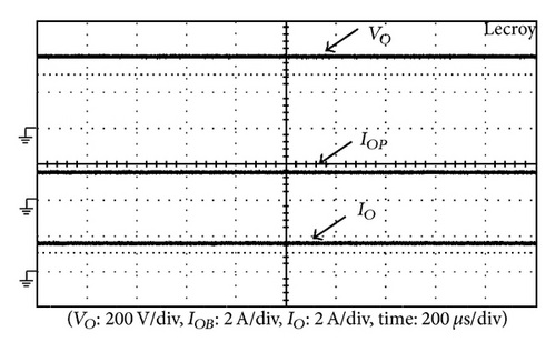
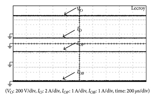
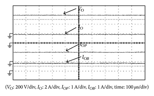
The operational conditions of the proposed PV power conversion systems in mode VIII of (PPV(max ) + PB(max )) ≥ PL can be divided into two conditions: PPV(max ) ≥ PL and PPV(max ) < PL. The measured waveforms of output voltage VO, currents IOP, IOB, and IO under PPV(max ) = 700 W and PL = 500 W are shown in Figure 17. In this operational condition, current IOP is equal to IO and IB is equal to 0. That is, the proposed boost converter with MPPT is used to supply power to load and PV arrays are not operated at MPP, while the proposed boost one with voltage regulation is shut down. When PPV(max ) < PL, the measured output voltage VO and currents IOP, IOB, and IO under PPV(max ) = 400 W and PL = 700 W are shown in Figure 18, illustrating that output voltage VO is still clamped at 400 V and IO = IOP + IOB. The experimental results show that both of the proposed PV power conversion systems with the single-capacitor snubber and with boost type snubber can implement power management.
5. Conclusion
In this paper, an interleaved coupled-inductor boost converter with different soft-switching snubbers is proposed for PV arrays applications. To compare the performances of the proposed converter with the single-capacitor snubber or with the boost type snubber, MPPT algorithm, power management, and control design of the proposed PV power conversion system have been firstly described in detail. In addition, a perturbation-and-observation method is used to implement the MPPT algorithm. For further evaluating the performances and feasibilities of the proposed PV power conversion system, prototypes of PV power conversion system with different soft-switching snubbers and with specifications of PPV(max ) = 1.2 kW and PVB(max ) = 1.2 kW have been built. Experimental results have shown that the proposed converter with boost type snubber can yield higher efficiency than the ones with the single-capacitor snubber and with hard-switching circuit, where the conversion efficiencies for converter with single-capacitor snubber and boost type snubber are 86% and 90% under full load, respectively. Therefore, the proposed interleaved coupled-inductor boost converter with the single-capacitor snubber is suitable for PV arrays applications with a lower cost, while the proposed one with boost type snubber is applied to PV arrays for a higher conversion efficiency power conversion system.


