A High-Speed and Low-Energy-Consumption Processor for SVD-MIMO-OFDM Systems
Abstract
A processor design for singular value decomposition (SVD) and compression/decompression of feedback matrices, which are mandatory operations for SVD multiple-input multiple-output orthogonal frequency-division multiplexing (MIMO-OFDM) systems, is proposed and evaluated. SVD-MIMO is a transmission method for suppressing multistream interference and improving communication quality by beamforming. An application specific instruction-set processor (ASIP) architecture is adopted to achieve flexibility in terms of operations and matrix size. The proposed processor realizes a high-speed/low-power design and real-time processing by the parallelization of floating-point units (FPUs) and arithmetic instructions specialized in complex matrix operations.
1. Introduction
In recent years, multiple-input multiple-output orthogonal frequency-division multiplexing (MIMO-OFDM) has been attracting attention as a scheme for achieving high-speed and large-capacity wireless communications. MIMO-OFDM has been adopted for the current wireless LAN standard, IEEE 802.11n [1], and for the next-generation wireless LAN standard, IEEE 802.11ac [2].
It is possible to increase the communication capacity in MIMO systems by increasing the number of transmit and receive antennas; however, communication quality is degraded by the consequent multistream interference. As a solution to this degradation problem, singular value decomposition (SVD) MIMO systems are used. In the case of SVD-MIMO systems, it is possible to suppress multistream interference and to improve communication quality with beamforming using SVD [3]. The implementation of SVD by applying custom hardware processors has been reported in recent studies [4–7]. These processors provide high-speed calculation and enough accuracy for 4 × 4 SVD-MIMO systems. However, SVD-MIMO systems require not only SVD calculation but also other operations such as compression and decompression of feedback matrices [8] and should support a variety of matrix sizes depending on their configuration. Additionally, applying dedicated hardware only to SVD calculation is not superior in terms of utilization efficiency. Therefore, we have employed an application specific instruction-set processor (ASIP) architecture to achieve both flexibility and high processing efficiency. The ASIP implementation of QR decomposition supporting MIMO systems has been presented in [9]. However, it does not support SVD-MIMO systems.
This study mainly deals with 4 × 4 SVD-MIMO-OFDM systems; in particular, flexible processor supporting SVD of MIMO channel matrices and compression/decompression of feedback matrices was designed. The processor achieves efficient, real-time processing by parallelization of floating-point units (FPUs) and arithmetic instructions specialized in complex matrix operations. Since the processor employs an ASIP architecture and a floating-point data format, it can deal with other operations and larger matrix sizes (e.g., 8 × 8) while keeping high calculation accuracy. The improvement compared to our previous work [10] has been achieved by simplifying FPUs and optimizing calculation bit length. Additionally, a “packet-skip” method for reducing energy consumption and improving communication throughput is proposed and evaluated.
This paper is organized as follows. The theory of SVD-MIMO systems is explained in Section 2, and the algorithm of SVD and matrix compression/decompression is described in Section 3. Section 4 explains the structure of the proposed processor. Section 5 presents the evaluated performance of the designed circuit. The packet-skip method is explained and evaluated in Section 6. Section 7 presents the conclusions drawn from this study.
2. SVD-MIMO System
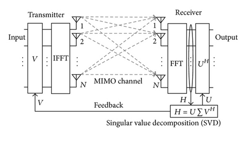
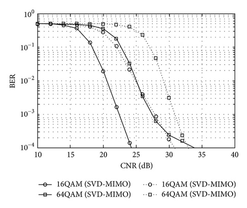
To investigate the effect of SVD-MIMO on improving transmission performance, bit error rates (BERs) of space-division multiplexing (SDM) MIMO without beamforming and of SVD-MIMO are compared by a baseband simulation. A 4 × 4 MIMO-OFDM system was used for this BER comparison. The simulation parameters are listed in Table 1 and the characteristics of SDM-MIMO and SVD-MIMO are compared in Figure 2. The figure shows that the beamforming by SVD-MIMO gains about 3 to 5 dB in carrier to noise ratio (CNR) for BER of 10−3.
| Channel bandwidth | 40 MHz |
| Number of FFT/IFFT points | 128 |
| Number of data subcarriers | 108 |
| Guard-interval duration | 800 ns |
| Packet size | 500 bytes |
| Modulation mode | 16QAM, 64QAM |
| Coding rates | 3/4 |
| MIMO-channel model | TGn channel model D |
| Feedback-channel model | Ideal |
3. Algorithm
3.1. Singular Value Decomposition
- (a)
Bidiagonalization : calculate upper bidiagonal matrix B by bidiagonalization using a Householder transformation.
- (b)
SVD of bidiagonal matrix : execute eigenvalue decomposition of by a QR algorithm and calculate U2 = BV2Σ−1 from V2, Σ.
- (c)
Inverse transform U = U1U2, V = V1V2: calculate unitary matrices U and V from U1 and U2 and V1 and V2, respectively, in steps (a) and (b).
3.1.1. Eigenvalue Decomposition by QR Algorithm
3.2. Feedback-Matrix Compression
| Noncompressed | Compressed |
|---|---|
| 24192 bit | 7776 bit |
4. Processor Structure
An application specific instruction-set processor (ASIP) architecture has been employed for the processor architecture, and efficient processing and flexibility were achieved by preparing arithmetic instructions specialized in complex matrix operations.
4.1. Circuit Structure
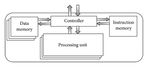
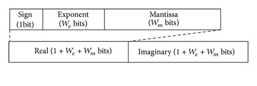
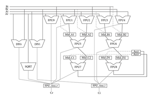
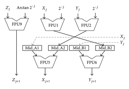
The circuit structure of the proposed processor is illustrated in Figure 3. Data and instructions are stored to each memory unit, and the processing unit executes instructions in order. The floating-point data format supports complex values, and each part of a complex value consists of a 1-bit sign part, a We-bits exponent part, and Wm-bits mantissa part, whose format is shown in Figure 4. Basically, each bit length is based on the IEEE 754 standard (We = 8, Wm = 23). Data memories and processing units are arrayed by the number of parallel processing. Two types of data transfers, which are shown in Figure 5, are supported. A single-data transfer sends data to the processing unit one by one. On the other hand, a block-data transfer sends data blocks containing multiple entries to the processing unit. The structure of the processing unit, which consists of nine floating-point units (FPUs) and dedicated circuits for division and square-root operation [11], is shown in Figure 6. “FPU1” to “FPU4” are used for multiplication, and “FPU5” to “FPU9” are used for addition and subtraction; in particular, “FPU9” is used for only CORDIC operations, which are described in Section 4.4. A variety of instructions can be executed by changing the data paths in the processing unit.


4.2. Instruction Format
The instruction format consists of memory addresses of input data A, B, output data C, and operation type, whose format is shown in Figure 7. The bit lengths are given as log 2 NDW bits and log 2 NOP bits, where NDW is the number of data memory words, and NOP is the number of instructions. Table 3 lists the instructions supported by the proposed processor.
| Index | Operation |
|---|---|
| 0 | Complex addition |
| 1 | Complex subtraction |
| 2 | Complex multiplication |
| 3 | Real multiplication |
| 4 | Accumulative complex addition |
| 5 | Accumulative complex subtraction |
| 6 | Accumulative complex multiplication |
| 7 | Accumulative real multiplication |
| 8 | Real division |
| 9 | Square-root operation |
| 10 | Squared absolute value |
| 11 | Accumulative squared absolute value |
| 12 | Hermitian multiplication |
| 13 | Initialization for the Newton method |
| 14 | Complex conjugate |
| 15 | Data copy |
| 16 | Initialization in CORDIC arctangent |
| 17 | Repetition in CORDIC arctangent |
| 18 | Initialization in CORDIC sine and cosine |
| 19 | Repetition in CORDIC sine and cosine |
| 20 | Merge real and imaginary parts |
| 21 | Extraction of real part |
| 22 | Extraction of imaginary part |
| 23 | Extraction of sign parts |
| 24 | Conversion from integer to floating-point format |
| 25 | Conversion from floating-point format to integer |

4.3. Complex Operation
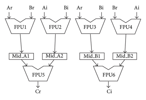
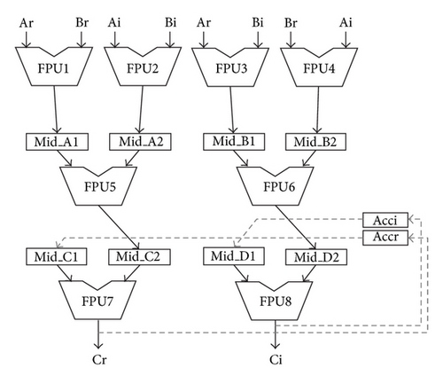
The proposed processor achieves efficient processing in complex matrix operations by adopting specialized instructions and an operation-unit structure. For instance, the complex multiplication of A × B = (Ar + jAi)(Br + jBi) = (ArBr − AiBi) + j(ArBi + AiBr) = Cr + jCi = C is executed in seven cycles using “FPU1” to “FPU4,” “FPU5,” and “FPU6” for multiplication, subtraction and addition, respectively, as shown in Figure 8. Moreover, the accumulative complex multiplication is executed in nine cycles using the registers of “Accr”, “Acci,” and “FPU7,” and “FPU8” as shown in Figure 9.
4.4. CORDIC Method
4.5. Division and Square-Root Operation
In the case that only “FPU1” to “FPU8” are used, the division and square-root operations are executed by approximate calculation using the Newton-Raphson method. However, they require 115 cycles and 1430 cycles, respectively. The implementation of dedicated circuits for division and square-root operation is effective for hardware acceleration. Division and square-root floating-point units [11] were therefore adopted. Since those units can execute division and square-root operation in 11 cycles, calculation time can be significantly reduced.
4.6. Bit-Length Optimization
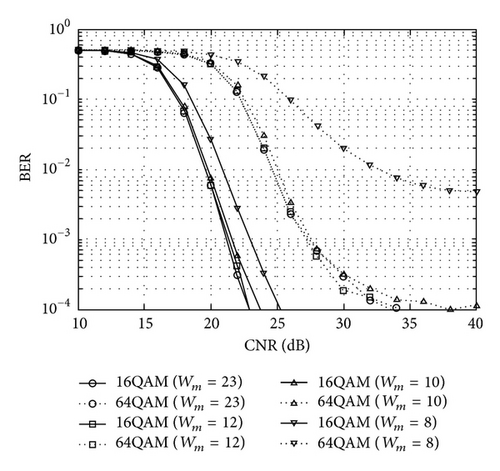
Since required precision depends on systems, circuit area and power consumption can be reduced by decreasing bit length. To optimize the mantissa bit length of the proposed processor for SVD and matrix compression/decompression, BER characteristics for several bit lengths were evaluated by simulation. The simulation parameters are the same as listed in Table 1, and the characteristics evaluation is shown in Figure 11. From this figure, the optimal mantissa bit length is taken as 12 bits.
5. Performance Evaluation
5.1. Circuit Design
The proposed processor was designed by using Verilog hardware description language and synthesized in the controller and the processing units by using a 90 nm CMOS standard cell library. The clock frequency was set to 400 MHz (2.5 ns in a clock period), and the supply voltage was set to 1.0 V.
5.2. Circuit Performance
The circuit performance was evaluated in cases with or without division and square-root units. The results are listed in Tables 4 and 5, respectively. The calculation time for all channel matrices of 108 data subcarriers was measured. The number of entries in the block data transfer was set to 18 to minimize energy consumption. According to these results, the implementation of the division and square-root units increases circuit area two-fold and power consumption by half. However, since the calculation time can be reduced to 1/7 ~ 1/9, energy consumption can be reduced to 1/4 ~ 1/6. This comparison shows that the implementation of division and square-root units is effective.
| Single | Block (18 entries) | |
|---|---|---|
| Calculation time (ms) | 6.33 | 1.16 |
| (per matrix) | (0.06) | (0.01) |
| Gate count | 82,376 | 90,885 |
| Power consumption (mW) | 22.1 | 39.4 |
| Energy consumption (μJ) | 139.9 | 45.8 |
| (per matrix) | (1.3) | (0.4) |
| Single | Block (18 entries) | |
|---|---|---|
| Calculation time (ms) | 46.92 | 10.45 |
| (per matrix) | (0.43) | (0.10) |
| Gate count | 38,688 | 47,390 |
| Power consumption (mW) | 13.5 | 25.4 |
| Energy consumption (μJ) | 633.0 | 265.1 |
| (per matrix) | (5.9) | (2.5) |
5.3. Bit-Length Limitation
In the previous section, circuit performance without bit length limitation (Wm = 23) was evaluated. In contrast, in this section, circuit performance with bit length limitation (Wm = 12) is evaluated (see Table 6). In this evaluation, division and square-root units were implemented and the bit-length limitation is applied in multipliers only, which account for large portion of the operation. This result shows that the bit-length limitation can reduce circuit area, power consumption, and energy consumption by about 10%, 20%, and 20%, respectively.
| Single | Block (18 entries) | |
|---|---|---|
| Calculation time (ms) | 6.33 | 1.16 |
| (per matrix) | (0.06) | (0.01) |
| Gate count | 73,564 | 81,943 |
| Power consumption (mW) | 18.5 | 30.8 |
| Energy consumption (μJ) | 117.0 | 35.8 |
| (per matrix) | (1.1) | (0.3) |
5.4. Processing Time
A timing chart of the SVD-MIMO-OFDM system is shown in Figure 12. It is assumed that the update and feedback of CSI are executed at every packet. The calculation of SVD and the matrix compression must be completed between receiving the preamble of the data packet and sending the feedback-matrix data. When the number of OFDM data symbols, NSYM, is 50, the acceptable calculation time is 252 μs. When the proposed processor arrays six processing units by parallel processing, it takes 193 μs for SVD and matrix compression. Since the calculation time is less than the acceptable calculation time, the processor realizes real-time processing.

5.5. Comparison with Related Works
The proposed processor is compared here with our previous work [10] and other related works [4–6] in Table 7. Compared with our previous work, the proposed processor has improved throughput by almost four times, even though it also performs matrix compression. This improvement was achieved by simplifying FPUs and imposing the bit-length limitation. In consideration of SVD operation only, the performance of the proposed processor is not superior to that of either [5] or [6]. However, it can realize sufficient real-time processing and support not only SVD but also matrix compression and decompression (MCD). It therefore achieves faster communication throughput than the other processors. Furthermore, since the proposed processor employs an ASIP architecture and floating-point data format, it can deal with other operations and larger matrix sizes while keeping high calculation accuracy. Given these advantage features, it is concluded that the proposed processor can realize an SVD-MIMO-OFDM system more effectively than the other processors.
| [4] | [5] | [6] | [10] | Proposed | |
|---|---|---|---|---|---|
| Architecture | Custom | Custom | Custom | ASIP | ASIP |
| Data type | fixed point | fixed point | fixed point | floating point | floating point |
| Matrix size | 4 × 4 | 4 × 4 | 4 × 4 | 4 × 4 | 4 × 4 |
| CMOS process | 90 nm | 0.18 μm | 90 nm | 90 nm | 90 nm |
| Gate count | 900 k | 42.3 k | 120 k | 83.7 k | 81.9 k |
| Clock frequency (MHz) | 500 | 149 | 182 | 400 | 400 |
| Throughput (matrices/s) | 125 k | 303 k | 7 M | 25 k | 93 k |
| Calculation time (μs/matrix) | 8 | 3.3 | 0.14 | 40 | 10.8 |
| Utilization efficiency (throughput/gate count) | 0.15 | 7.16 | 59.52 | 0.29 | 1.13 |
| Supported operations | SVD | SVD | SVD | SVD | SVD, MCD |
| Size of side information | Large | Large | Large | Large | Compressed |
6. Packet-Skip Method
As explained in the previous sections, it was assumed that the system feeds back the weight matrix at every packet. However, if the channel state is changed gradually, it is possible to skip the SVD calculation and the feedback of the weight matrix and to apply the previous weight matrix without degradation of BER. On the basis of this idea, energy consumption can be reduced and communication throughput can be increased by skipping the SVD calculation and the weight-matrix feedback.
6.1. Simulation
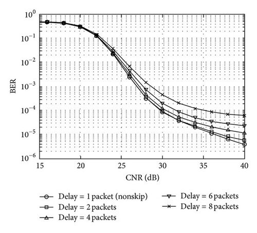
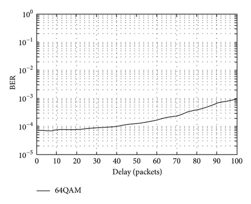
To determine the optimal skip number, BER characteristics for several numbers of packet skips were evaluated by simulation. The simulation assumed a communication environment with the 10 Hz Doppler frequency. The simulation parameters are listed in Table 8, and the BER evaluation result is shown in Figure 13. The delay in this figure means the numbers of packet skips. The packet skip is applied from the packet at which the SVD calculation process starts to the packet to which weight matrices are applied. According to this figure, a delay of less than 5 packets is acceptable under this communication environment. Additionally, BER characteristics in a communication environment with the 1 Hz Doppler frequency were evaluated. The simulation parameters are listed in Table 9, and the BER evaluation result is shown in Figure 14. According to this figure, a delay within 30 to 40 packets is acceptable under this communication environment.
| Channel bandwidth | 40 MHz |
| Number of FFT/IFFT points | 128 |
| Number of data subcarriers | 108 |
| Guard-interval duration | 800 ns |
| Number of OFDM symbols | 50 |
| Modulation mode | 64QAM |
| Coding rates | 3/4 |
| MIMO-channel model | TGn channel model D |
| Doppler frequency | 10 Hz |
| Feedback-channel model | Ideal |
| Channel bandwidth | 40 MHz |
| Number of FFT/IFFT points | 128 |
| Number of data subcarriers | 108 |
| Guard-interval duration | 800 ns |
| Number of OFDM symbols | 50 |
| Modulation mode | 64QAM |
| Coding rates | 3/4 |
| MIMO-channel model | TGn channel model D |
| Doppler frequency | 1 Hz |
| CNR | 30 dB |
| Feedback-channel model | Ideal |
6.2. Skip Method
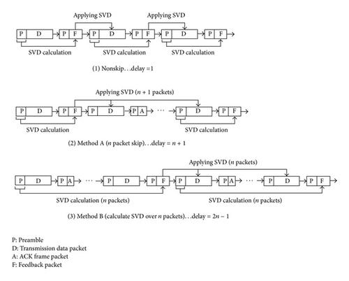
For packet skipping, two methods (illustrated schematically in Figure 15) are proposed. As for the first method, that is, method A, SVD calculation is executed over one packet and the weight matrices are applied to the next (n + 1) packets. The delay produced by method A is (n + 1) packets. On the other hand, as for the second method, that is, method B, SVD is calculated over n packets, and the weight matrices are applied to the n packets after the SVD calculation. The delay produced by method B is (2n − 1) packets. In the case of method A, total energy consumption is reduced by 1/(n + 1). In the case of method B, the power consumption can be reduced since the calculation time of SVD is longer than that of the nonskip system or method A.
6.3. Performance Evaluation
Circuit performance and communication throughput when these skip methods were applied was evaluated. In the evaluation, it was assumed that the delay is 5 packets for a communication environment with the 10 Hz Doppler frequency. Accordingly, n = 4 and 3 for methods A and B, respectively. The results of the performance evaluation are listed in Table 10. In the evaluation, communication throughput was calculated under the assumption that signals are transmitted by 4 × 4 SVD-MIMO (64QAM, R = 3/4, and 50 symbols) and the feedbacks are transmitted by 4 × 4 SDM-MIMO (16QAM, R = 3/4). According to these performance results, method A is the most effective in terms of energy consumption and communication throughput.
| Nonskip | Method A | Method B | |
|---|---|---|---|
| Acceptable calculation time (μs) | 252 | 252 | 836 |
| Number of parallel ASIPs | 6 | 6 | 2 |
| Calculation time (μs) | 193.7 | 193.7 | 581.2 |
| Energy consumption (per packet) (μJ) | 35.82 | 7.16 | 11.94 |
| Communication throughput (Mbps) | 292.8 | 324.0 | 318.3 |
7. Concluding Remarks
A processor design for SVD-MIMO-OFDM systems was proposed. The proposed processor employs an ASIP architecture and achieves both flexibility and high throughput by parallelization of FPUs and arithmetic instructions that are specialized in complex matrix operations. In addition, two types of packet-skip method for reducing energy consumption and increasing communication throughput were proposed. In future work, we will deal with larger-scale SVD-MIMO-OFDM systems (e.g., 8 × 8 SVD-MIMO).


