The Effect of Annealing on the Structural and Optical Properties of Titanium Dioxide Films Deposited by Electron Beam Assisted PVD
Abstract
Titanium dioxide thin films were deposited on crystalline silicon substrates by electron beam physical vapor deposition. The deposition was performed under vacuum ranging from 10−5 to 10−6 Torr without process gases, resulting in homogeneous TiO2−x layers with a thickness of around 100 nm. Samples were then annealed at high temperatures ranging from 500°C to 800°C for 4 hours under nitrogen, and their structural and optical properties along with their chemical structure were characterized before and after annealing. The chemical and structural characterization revealed a substoichiometric TiO2−x film with oxygen vacancies, voids, and an interface oxide layer. It was found from X-ray diffraction that the deposited films were amorphous and crystallization to anatase phase occurred for annealed samples and was more pronounced for annealing temperatures above 700°C. The refractive index obtained through spectroscopic ellipsometry ranged between 2.09 and 2.37 in the wavelength range, 900 nm to 400 nm for the as-deposited sample, and jumped to the range between 2.23 and 2.65 for samples annealed at 800°C. The minimum surface reflectance changed from around 0.6% for the as-deposited samples to 2.5% for the samples annealed at 800°C.
1. Introduction
Titanium dioxide (TiO2) has promising physical, chemical, and optical properties that make it an interesting material for a wide range of applications. TiO2 is a wide bandgap semiconductor with an indirect optical bandgap ranging from 3.2 eV—for the anatase phase to 3.0 eV—for the rutile phase [1]. The refractive index of the bulk crystal TiO2 ranges from 2.4 to 2.9 [2] which makes the material attractive for many optical applications including antireflective coatings for silicon based solar cells.
Several methods have been used to deposit TiO2 thin films on various substrates, including electron-beam evaporation [3–5], chemical vapor deposition (CVD) [6–8], pulsed laser deposition (PLD) [9], sputtering [10, 11], and sol-gel method [12–14]. The properties of deposited films, however, are highly dependent on the processing techniques and the deposition conditions [3, 4, 15–17].
Electron beam (e-beam) evaporation is one of the techniques used to deposit uniform and high quality titanium oxide coatings [2, 17] but still needs to be investigated explicitly due to its importance as a technique that can be used to produce antireflective coatings on an industrial scale for many applications, including solar cells. As-deposited, e-beam evaporated films are usually amorphous [4, 17]. In addition, it has been reported that such TiO2 films have a degree of porosity and their refractive index is significantly lower than the bulk material [2, 5, 13].
Usually depositing titanium dioxide layers by e-beam physical vapor deposition (PVD) is carried out in the presence of oxygen as process gas in order to substitute the loss of oxygen that results from heating the source by the electron beam [3]. Therefore, it is expected that during e-beam evaporation of titanium dioxide, the vapor would contain various mixtures of titanium oxide at different oxidation states, resulting in layers with varying properties [18]. It has been shown in the literature that in order to obtain homogenous, stoichiometric TiO 2 films, the deposition must be in the presence of oxygen gas or the evaporation material should start from TiO or reactive Ti [3, 19]; otherwise, substoichiometric (TiO2−x) or lower oxidation state titania structures (e.g., TiO or Ti2O3) would be obtained [3, 19].
Little work is reported on the effect of annealing on the nanoscale properties of TiO2−x films deposited on c-Si by e-beam deposition without the presence of oxygen and without ion-beam assistance. It is expected that postdeposition thermal annealing would be essential for film densification and smoothening of the surface by forming polycrystalline anatase film with large grains and a preferred crystal orientation [20].
The present study deals with the characterization of TiO2−x films deposited by e-beam evaporation, followed by postdeposition annealing. The deposition is carried out at a relatively low pressure (in the 10−5–10−6 Torr range). In contrast to previous work presented in the literature [3, 4, 21], the deposition is done without the presence of oxygen, or any other process gas, and without ion-beam assistance. Postdeposition thermal annealing is performed in nitrogen at the temperature range of 500°C to 800°C. Characterization by several methods—including X-ray diffraction (XRD), X-ray photoelectron spectroscopy (XPS), scanning electron microscopy (SEM), scanning transmission electron microscopy (STEM), atomic force microscopy (AFM), spectroscopic ellipsometry (SE), and reflectance spectrophotometry—reveals the impact of thermal annealing on the optical, structural, and chemical properties of the films.
2. Experimental Procedure
2.1. Sample Preparation
The starting substrates consisted of four-inch diameter Czochralski (100) single crystalline p-type silicon wafers. Prior to deposition, the wafers were cleaned by a standard RCA procedure which involves an organic clean with an H2O-H2O2-NH4OH solution, an oxide strip using an H2O-HF solution, and an ionic clean using a solution of H2O-H2O2-HCl. TiO2−x films were deposited on the surface of the wafers in a vacuum deposition system (Edwards AUTO 306, Edwards, UK) at a deposition pressure ranging from 10−5 to 10−6 Torr without introducing any process gas. The evaporation source was TiO2 pellets with 99.9% purity (Pure Tech. Inc., USA). Samples under investigation consisted of (1) as-deposited sample (labeled TAD) and (2) samples that have been subjected to a postdeposition thermal annealing in a quartz tube furnace under nitrogen flow at a mass flow rate of about 1 SLPM. The nitrogen gas introduced into the furnaces was a grade 3 (99.999% purity) from a liquid nitrogen source to avoid water condensates within the nitrogen container, which ensures that the nitrogen introduced into the annealing process was as dry as possible. Annealing was performed at temperatures from 500°C to 800°C in steps of 100°C. Samples T500, T600, T700, and T800 were labeled according to their annealing temperature. For the annealed samples, the furnace was brought to the set temperature of interest and the sample was gradually inserted and then pushed to the center of the furnace to ensure temperature uniformity. All samples were annealed for 4 hours before they were gradually pulled out of the furnace and cooled down before characterization.
2.2. Characterization
SEM, STEM, and EDS analyses of as-deposited samples were performed using a JSM7600F FE-SEM and a JEM-2100F TEM—in private communication with JEOL Ltd., Tokyo, Japan. Cross sectional samples for these characterization methods were prepared using a special technique in which a low-energy argon ion beam irradiates the sample at small angles using an ion slicer. Such a technique reduces damage artifacts of the sample such as amorphisation, recrystallization, or phase changes that are usually encountered with conventional ion-beam milling [23].
XPS was used to reveal subtle chemical and electronic properties of deposited films. On top of the atomic species present in the sample, XPS spectra were used to reveal oxidation states. The XPS measurements were carried out on a Thermo ESCALAB 250 Xi (Thermo Scientific, UK) using Al-K-alpha radiation at 1486.6 eV. The sample was introduced into the load-lock chamber with the sample holder and was transferred into the analysis chamber where the vacuum was in the 10−9–10−10 mBar range. A flood gun with standard charge compensation mode was used to neutralize the charge build-up on the surface of insulating samples. The samples were kept in a desiccator before being introduced into the XPS vacuum chamber through a load-lock system. Spectra acquisition and processing were carried out using Thermo Avantage software. Detailed XPS analyses were performed for Ti2p, O1s, Si2p, and C1s core levels for as-deposited films and films annealed at various temperatures up to 800°C. Carbon C1s spectra are usually present in all samples due to surface contamination. The C1s peaks can serve as a reference to correct shifts in the spectra that can arise from electrostatic charging on the surface of samples [21, 25]. All XPS measurements are within an error of (+/−) 0.2 eV.
Optical reflectance spectra of TiO2−x thin films were measured using a Shimadzu SolidSpec-3700 UV-Vis-NIR Spectrophotometer (Shimadzu, Japan) in the wavelength range from 200 nm to 1200 nm. An integrating sphere was used to measure total diffusive and specular reflectance and the condition for minimum reflectance for all films was compared to reveal changes due to annealing. A BaSO4 white plate was used as the reflectance standard.
3. Results and Discussion
3.1. X-Ray Diffraction
Powder XRD data for the as-deposited and annealed films are shown in Figure 1. The XRD spectra reveal a TiO2−x film with an amorphous nature for the as-deposited sample (TAD). Crystallization to an anatase structure is observed for samples annealed at 500°C and above, as shown in Figure 1. The crystalline structure of the annealed TiO2−x films remains unchanged up to an annealing temperature of 800°C. For the sample annealed at 800°C (T800), more pronounced anatase peaks at 2θ = 25.4° and 37.8° are noticed. Interestingly, no rutile phase is evident in any of the films even for annealing temperatures as high as 800°C.
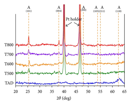
The primary crystallite size calculated for annealed samples from the Scherrer equation is listed in Table 1. The crystallite size becomes larger as the annealing temperature increases. It was found that our films exhibited slower crystallization even at high annealing temperatures, when compared to other work in the literature [14, 28, 29]. What is also interesting is that no transformation from anatase to rutile was observed in any of our studied films. The observed crystallization behavior of the TiO2−x films under different annealing temperatures could be due to an unclear effect of substrate (as mentioned in [2, 11, 16]), due to the level of oxygen defects in the initially deposited films [25], or speculatively due to oxidation of the silicon substrate.
| Sample | Primary crystallite size (nm) | Surface roughness (nm) | Layer thickness from SE (nm) | Reflectivity % | Minimum reflectance wavelength (nm) |
|---|---|---|---|---|---|
| TAD | — | 0.73 | 96.1 ± 0.2 | 0.64 | 758 |
| T500 | 13.4 | 0.74 | 87.3 ± 0.1 | 0.40 | 706 |
| T600 | 15.1 | 0.88 | 86.8 ± 0.1 | 0.41 | 712 |
| T700 | 18.7 | 0.77 | 88.1 ± 0.1 | 0.43 | 718 |
| T800 | 26.6 | 2.74 | 79.5 ± 0.1 | 2.49 | 744 |
3.2. X-Ray Photoelectron Spectroscopy
XPS spectra for the Ti2p core levels and for oxygen O1s core electrons for all the samples are displayed in Figure 2. The Ti2p core level spectrum shows that titanium is present at the Ti4+ state corresponding to binding energies of 458.6 (+/−) 0.2 eV and 464.4 (+/−) 0.2 eV for the Ti2p3/2 and Ti2p1/2 peaks, respectively, for all films, as-deposited and annealed. Binding energies obtained are very close to those obtained in the literature for Ti4+ corresponding to TiO2 [21, 25]. Furthermore, a Gaussian-Lorentzian curve was fitted to the experimental data showing a single peak Gaussian-Lorentzian profile, which reveals that titanium exists within all films as Ti4+ belonging to TiO2.


The O1s spectrum shows two major peaks that were identified by a multipeak Gaussian-Lorentzian fit of the XPS spectrum in the energy range from 525 eV to 535 eV. The first major peak (O1sa) occurred at 529.8 (+/−) 0.2 eV corresponding to O-Ti binding in the titanium oxide structure [21, 25]. Another O1s peak (O1sb) is evident at around 530.9 (+/−) 0.2 eV for all annealed samples while the peak position for the as-deposited sample (TAD) is at 532 eV. Those peaks can be identified with hydrocarbon or hydroxy species present as contaminants on the surface [21, 25]. XPS spectra have also revealed a weak silicon peak at around 101.9 eV—not shown here—that can be due to sample preparation.
A detailed XPS study of TiO2−x films grown by sputtering in an oxygen rich environment from a TiO2 target on crystalline silicon by Laidani et al. [25] revealed three main O1s peaks at binding energies of 529.75 eV, 531.01 eV, and 532.01 eV. The three peaks were identified as belonging to titanium oxide, hydroxy group binding to Ti and a carbon-oxygen type bonding from surface contamination, respectively.
A third smaller peak has been identified by the de-convolution of the overall O1s spectrum for the sample annealed at 600°C (T600) at a binding energy of 532.7 eV. This smaller peak is speculatively attributed to a silicon-oxygen bond [21, 30]. An XPS scan of the silicon Si2p spectrum—not shown here—shows a peak at 103.5 eV for sample T600 that can correspond to silicon oxide bonding.
Atomic percentages of titanium (Ti2p) and oxygen (O1s) were calculated from the peak areas for all samples. The atomic ratio of oxygen bonded to titanium (O1sa) to titanium (Ti2p3/2) atomic percentage gives the stoichiometry (x) of the TiO2−x structure [25]. Table 2 summarizes the atomic percentages calculated from the Ti2p and O1s XPS data.
| Sample | Ti2p3/2 atomic % | O1s(a) atomic % | O1s(a): Ti2p3/2 ratio |
|---|---|---|---|
| TAD | 11.1 | 32.4 | 2.92 |
| T500 | 17.91 | 29.41 | 1.64 |
| T600 | 16.69 | 25.09 | 1.50 |
| T700 | 14.38 | 21.73 | 1.51 |
| T800 | 10.51 | 19.04 | 1.81 |
Results summarized in Table 2 show a substoichiometric structure for all samples except the as-deposited (TAD), where excess oxygen (x > 2) could be due to either an oxygen rich film—as was observed by Jang et al. [3]-, or to an unknown contamination source on the surface although this rarely is the case. Jang et al. have reported titanium oxide films that were oxygen-rich as was revealed by XPS and oxygen resonance backscattering spectroscopy (ORBS), even when grown under no oxygen flow.
One interesting observation is that the atomic ratio of O1sa—belonging to the TiO2−x structure—to Ti2pa shows an increase from 1.51 to 1.81 as the annealing temperature goes from 700°C to 800°C. We speculate that this could be due to the filling of oxygen defects, assisted by the crystallization process since annealing is taking place in ambient conditions where oxygen is present. This further demonstrates the importance of this temperature range where several properties of the TiO2−x film show an abrupt change. The main observation from the XPS results is that the titanium spectra represent a single Ti4+ peak at a binding energy that corresponds to its bonding with oxygen within the TiO2−x structure, where the Ti4+ oxidation state remains unchanged for all samples annealed up to 800°C. Additionally, it was found that annealed films were oxygen deficient with a large fraction of oxygen defects within the TiO2−x structure causing those films to become substoichiometric. Therefore, growing TiO2 films by electron beam evaporation without the introduction of oxygen as a process gas starting from a TiO2 source seems to affect the stoichiometry of films rather than the oxidation state of titanium.
The as-deposited sample (TAD) was an exception showing an excess oxygen content that could in certain cases come from carboxyl type, surface contamination, or an oxygen rich layer, although the latter case is less likely since the growth conditions were poor in oxygen.
3.3. Scanning and Transmission Electron Microscopy
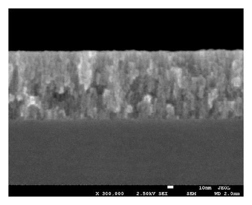
A cross sectional sample of the as-deposited TiO2−x film (TAD) was imaged under an FE-SEM at 300,000X. The SEM image (Figure 3) shows a film of a columnar structure with voids, typical of a physical vapor deposition process without ion-beam assistance, where the surface energy is not enough to promote surface diffusion of adatoms. This kind of film growth mechanism occurs when the condensate atoms do not have sufficient kinetic energy to overcome the surface energy. In that case, the resulting film is created by nucleation processes followed by coalescence that causes reorganization of the crystalline structure, guiding the growth in different orientations. This type of structure has been observed in many metal-oxide films grown by physical vapor deposition techniques [31, 32].
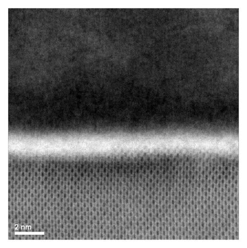
A scanning-transmission electron microscopy with energy dispersive spectroscopy (STEM/EDS) bright field image of the cross sectional sample is shown in Figure 4. The image clearly highlights an interface layer (bright) in between the crystalline silicon substrate and the top TiO2−x layer. The interface layer is a few nanometers thick within the precision of measurement.
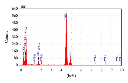
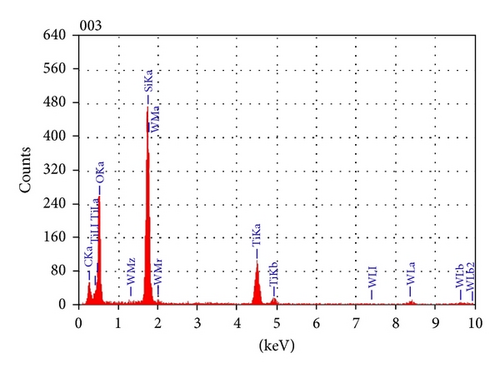
To reveal more about the chemical nature of the deposited film and the interface layer, an EDS analysis was performed on the film cross section. The EDS analysis showed that the bulk of the film consists mainly of titanium and oxygen (Figure 5). Carbon signal was also present that could have come from contamination on the surface due to sample preparation. A small tungsten signal was also present and is suspected to have come from the crucible (made of tungsten) that could have been eroded by a misaligned electron beam during deposition. EDS analysis performed on the interface layer reveals that it consists of silicon, oxygen, and titanium atoms, suggesting that this interface layer could be a mixture of silicon oxide and titanium oxide (Figure 6).
3.4. Atomic Force Microscopy
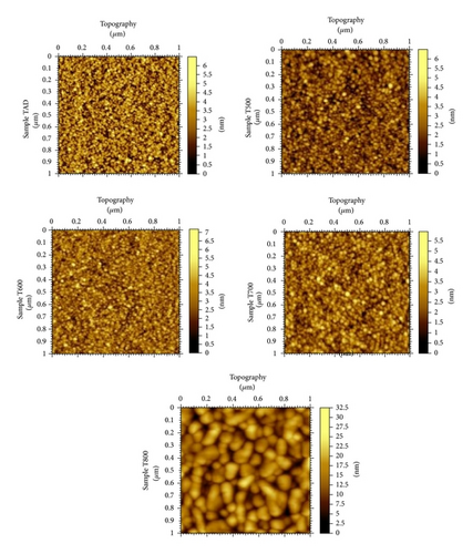
The AFM topography images for all samples obtained with a scan size of 1 × 1 μm2 are shown in Figure 7. The topography images reveal a surface morphology that remains almost unchanged for the as-deposited sample and for samples annealed at temperatures up to 700°C. For sample T800, annealed at 800°C, a sharp increase in surface roughness is observed in the topography image. This is believed to be due to film crystallization and grain growth. This conclusion can be deduced from the XRD data where samples annealed at 800°C showed a noticeable increase in crystallinity. Table 1 summarizes the surface roughness values for all samples, as computed according to our experimental procedure.
3.5. Spectroscopic Ellipsometry
The optical constants and film thicknesses are obtained for all samples under study using spectroscopic ellipsometry. The details of the measurement and the associated models and range of validity are described elsewhere [14]. Table 1 summarizes the values obtained for the film thicknesses. A reduction in film thickness by around 8 nm compared to sample TAD is observed for films annealed at up to 700°C. A further 8.6 nm reduction in thickness is observed for the sample T800 relative to T700. This reduction in thickness is due to film densification, crystallization, and grain growth. A similar behavior has been previously observed for TiO2 films deposited by other techniques, which underwent thermal treatment at elevated temperatures [7, 32, 33].
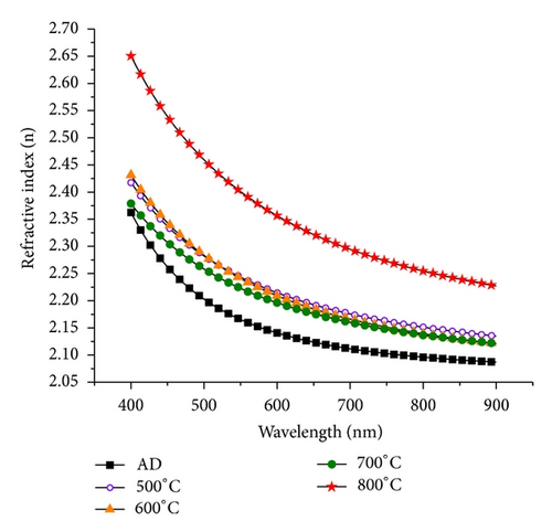
Ellipsometry results show an increase in the refractive index for the annealed samples (Figure 8). This increase can be explained by the onset of crystallization, as is evidenced by XRD. The results also clearly show a jump in the refractive index for the sample annealed at 800°C, which confirms that this annealing temperature is critical for the optical and structural properties of TiO2. Increase in the refractive index of TiO2−x films due to annealing at elevated temperatures has been demonstrated in the literature [28, 29, 32, 33] and is due to film crystallization, grain growth, film densification, and void fraction reduction [28, 33].
3.6. Reflectance Measurements
Figure 9 shows the total hemispherical reflectance measurement (including both diffuse and specular components) of the films under study for the wavelength range from 200 nm to 1200 nm. The minimum reflectance of the TiO2−x film along with the wavelength has been extracted from the measurements and is summarized in Table 1 (R6). The results show a large reduction in reflectance compared to the typical reflectance of a bare polished silicon surface (around 30%), with the minimum reflectance at a single wavelength, a behavior typical of single layer antireflective coatings (SLARs) [34].
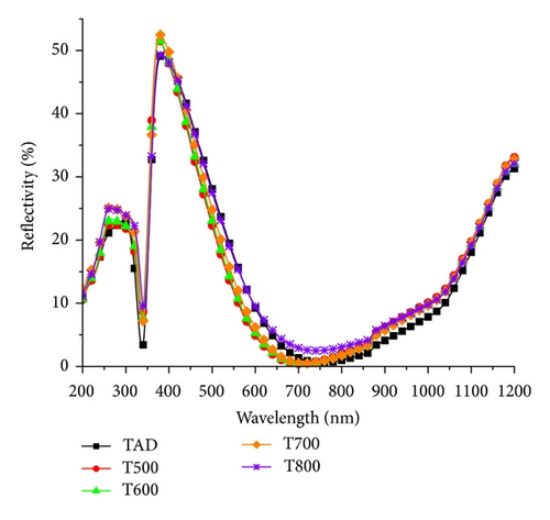
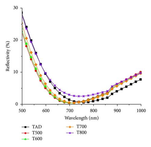
From the results summarized in Table 1, it is clear that the minimum reflectance along with the associated wavelength is slightly reduced for samples annealed at temperatures up to 700°C when compared to the as-deposited sample. This confirms the impact of film densification on the refractive index and film thickness. The reflectance properties of sample T800 show a sharp increase in the value and in the wavelength at minimum, due to changes in the optical constants of the film along with film thickness as was revealed by ellipsometry. Moreover, the change in surface roughness of annealed films—as revealed by AFM—also contributes to the increase in film reflectance.
4. Conclusions
- (1)
Growing TiO2−x films. with the Ti4+ oxidation state by electron beam assisted physical vapor deposition in the pressure range from 10−5 to 10−6 Torr without intentional introduction of oxygen as a process gas and without ion-beam assistance has been successful.
- (2)
The e-beam deposited films are amorphous and exhibit a columnar structure. An interface oxide layer in the range of 1-2 nm is also present in between the deposited films and the c-Si substrate.
- (3)
Chemical analysis by XPS revealed mainly substoichiometric TiO2−x films with no change in the oxidation state of titanium with annealing.
- (4)
TiO2−x films deposited by e-beam assisted PVD without introducing a process gas and without ion-beam assistance on c-Si substrates exhibit slow crystallization on the surface of the films even at high annealing temperatures. Surface morphology remains unchanged for all samples upon annealing at up to 700°C with a relatively small surface roughness, showing a partially crystalline nature.
- (5)
The films exhibit a drastic change in morphology with sharp increase in surface roughness when annealed at 800°C. For such an annealing temperature XRD and AFM analyses suggest a strong onset of crystallization and grain growth and the appearance of a more pronounced anatase crystalline structure.
- (6)
Ellipsometry measurements reveal a gradual change in optical properties and film thickness as annealing temperature is increased up to 700°C and confirm the presence of a sharp change in layer properties (refractive index and film thickness) for the sample annealed at 800°C.
- (7)
Reflectance spectrophotometry measurements show a drastic increase in reflectance for films annealed at 800°C compared to the as-deposited film and films annealed at up to 700°C, which is directly related to the increase in the refractive index due to film densification, rather than change in chemical structure.
In conclusion, it is confirmed that 800°C is a critical annealing temperature for TiO2 films deposited on c-Si by e-beam assisted PVD at which nanoscale structural and optical properties exhibit significant changes. It has been demonstrated that homogenous TiO2−x films can be grown on silicon substrates by electron beam deposition starting from a TiO2 target at high vacuum, without the introduction of oxygen as a process gas and without ion-beam assistance, as was confirmed by XPS measurements of as-deposited and annealed films.
Disclosure
This statement is to affirm that there is no direct financial relation between any of the commercial entities acknowledged in the paper (JEOL Ltd., Japan and Ashraf Co.) and any of the authors of this paper, and hence there should be no conflict of interests that could otherwise arise from such affiliations.
Acknowledgments
This work is supported by College of Engineering and Petroleum General Facility Grants GE01/07, GE01/08, and GE02/08, College of Science General Facility Grant GS02/08 for the use of the Thermo ESCALAB 250 Xi for XPS characterization and GS03/01, and the X-ray diffraction General Facility, provided by the research administration at Kuwait University. The authors would also like to thank Ashraf Co., Kuwait, and JEOL Ltd., Japan, for their help in completing the SEM and TEM work.


