Properties and Analysis of Transparency Conducting AZO Films by Using DC Power and RF Power Simultaneous Magnetron Sputtering
Abstract
DC power and RF power were introduced into the magnetic controlled sputtering system simultaneously to deposit AZO films in order to get an acceptable deposition rate with high quality transparency conducting thin film. The resistivity decreases with the RF power for the as-deposited samples. The resistivity of 6 × 10⁻⁴ Ω-cm and 3.5–4.5 × 10⁻⁴ Ω-cm is obtained for the as-deposited sample, and for all annealed samples, respectively. The transmittance of the AZO films with higher substrate temperature is generally above 80% for the incident light wavelength within 400–800 nm. The transmittance of the as-deposited samples reveals a clear blue shift phenomenon. The AZO films present (002) oriented preference as can be seen from the X-ray diffraction curves. All AZO films reveal compressive stress. The annealing process improves the electrical property of AZO films. A significant blue shift phenomenon has been found, which may have a great application for electrode in solar cell.
1. Introduction
High transparent metal oxide semiconductor with band gap larger than the energy of visible light is usually a good insulator at room temperature [1]. Impurities doping is the easy way to increase conductivity. Tin doped indium oxide (ITO) [2], aluminum doped zinc oxide (AZO) [3, 4], and fluorine doped tin oxide SnO2 : F (FTO) [5] are quite popular materials as transparent semiconductors. ITO, the best transparent conducting film, is a solid solution of indium (III) oxide (In2O3) and tin (IV) oxide (SnO2), typically 90% In2O3, 10% SnO2 by weight. However, with high cost and limited supplies of indium, alternatives are being sought. Another choice for transparency conducting film is FTO, which is widely used in dye-sensitized solar cell. However, it is very easy for hydrogen plasma to etch FTO, as well as tin oxide. The utilization of FTO and SnO2 in the thin film solar cell application is limited. AZO films are a good candidate as a transparent conductive material, because the materials (1) consist of cheap and abundant element, (2) are readily produced for large-scale coating, (3) allow tailing of ultraviolet absorption, (4) have a high stability in hydrogen plasma, and (5) have low growth temperature [6]. Besides, it is nontoxic and easy to fabricate. The reasons for higher conductivity of Al doped ZnO films can be attributed to extrinsic donor and intrinsic donor [7, 8]. The Al replaces Zn ions to form extrinsic donors, as well as from oxygen vacancies and Zn interstitial atoms to form intrinsic donor [7, 8]. Production of the high conductivity and high transparency AZO films by controlling the intrinsic defects is highly desired for industrial application. Fang et al. deposited AZO film at 320°C by the DC sputtering with postdeposition annealing at 400°C for 2 hours under 10−3 Pa and got the resistivity as low as 1.5 × 10⁻⁴ Ω-cm [6]. Park et al. used the RF sputtering method with 500°C high substrate temperature to get the lowest resistivity of 1.30 × 10⁻⁴ Ω-cm [9]. Kim et al. used a DC cosputtering method followed by rapid thermal annealing to achieve a low resistivity of 1 × 10⁻³ Ω-cm [10]. Ohta et al. investigated rapid thermal annealing of sputter-deposited ZnO and AZO films by using a radio-frequency (RF) argon thermal plasma jet at atmospheric pressure, and the lowest resistivity is around 3 × 10⁻⁴ Ω-cm [11]. Exarhos et al. used 30% O2/Ar gas mixture and 150 W RF sputtering method, followed by 4% hydrogen in argon 725 K annealing [12]. Chen et al. used 1.5% AZO target and O2/Ar gas mixture sputtering AZO film, followed by vacuum annealing, and analyzed its component with X-ray photoemission spectrum (XPS) and Auger electron spectrum (AES) [13]. Guillen et al. [14] used DC sputtering at room temperature, annealed it in vacuum at 350°C, and got the best resistivity of 8 × 10⁻⁴ Ω-cm. Lee [15] uses RF sputtering in H2 and Ar mixture which reaches a minimum value of 4.4 × 10⁻⁴ Ω-cm at the H2/(H2 + Ar) gas ratio of 2.5%. These AZO films are good choices for high conductivity and high transparency film. The AZO film made by RF sputtering seems to have better electrical property than that made by DC sputtering [16]. However, AZO film made by DC sputtering method has higher deposition rate than that made by RF sputtering method. Few factors will affect the quality, transparency, and conductivity of AZO films, such as grain size, crystallinity, and defects of different types [17]. In this work, we report the results of making AZO films using DC and RF sputtering simultaneous methods both as-deposited and annealed samples, to check their conductivity with acceptable deposition rate.
2. Materials and Methods
2.1. Specimen Preparation
Content of the target used in this work is 2 wt. % Al2O3 and 98 wt. % ZnO. A corning 1737 glass was used as a substrate. After cleaning, the target and the substrate were put into a magnetron sputtering system and evacuated to 6.7 × 10⁻³ Pa. Then Ar gas with 70 cm3/min flow rate was introduced into the reaction chamber. After turning on the DC power supplier and RF power supplier, the target was presputtering for 5 minutes to remove surface contamination. Then open the shutter and sputter for 30 min at the pressures of 2.7 × 10⁻¹ Pa. We have tested 3 different DC power suppliers to check the film quality with 30, 50, and 80 W and found that 80 W was the best choice for the film’s quality. Therefore, the DC power supplier was kept at 80 W, while the RF power was varied from 0 W to 120 W. Five substrate temperatures 225, 250, 275, 300, and 325°C were chosen for deposition. After deposition, one group of substrates was put into a high temperature furnace under a 550°C substrate temperature with 6% H2/Ar annealing for an hour to investigate the improvement of film quality. The thickness of films was measured by a Tencor alphastep 500 surface profiler, and the resistivity of films was measure by an ECOPIA model HMS-200 Hall Effect measurement system.
2.2. Crystalline Size
2.3. In-Plane Stress
2.4. Electrical Considerations
3. Results and Discussion
3.1. Structural Characteristics and Film Stress
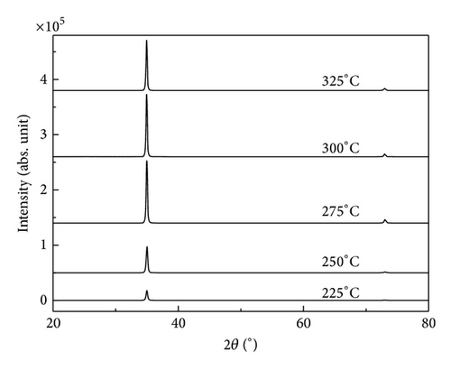
Figure 1 illustrates the X-ray diffraction (XRD) patterns for the AZO film. The XRD patterns were measured by the use of a Rigaku XRD model PC-2000. The full width at half maximum of the diffraction peak β1/2 and diffraction angle of the peak θ are determined from XRD patterns as illustrated in Figure 1. The diffraction peak intensity increases with the increasing substrate temperature, as can be seen from Figure 1. The increasing diffraction peak intensity of (002) between 225 and 325°C is primarily due to the crystallization of the AZO film.
The solid squares in Figure 2(a) give the thickness for the sputtered AZO films versus incident RF power. The thicknesses of the sputtered films are around 963–1412 nm. Obviously, the thickness increases with incident RF power for RF power ≤ 80 W but decreases with the incident RF power when RF power > 80 W. The increase of the thickness for RF power ≤ 80 W is primarily due to the increasing total incident power. That increases the ionization rate of the introduced Ar gas. The decrease of the thickness with the incident RF power, when RF power > 80 W, could be because positive cycle of the incident RF power is larger than the negative biased DC power (= 80 W). That decreases the ionization rate of the introduced Ar gas. The deposition rates for RF power = 0, 30, 50, 80, 100, and 120 W are 0.54, 0.59, 0.72, 0.79, 0.77, and 0.75 nm/s, respectively. The crystalline sizes of AZO films are also given in Figure 2(a), where the open squares indicate as-deposited samples and open triangles annealing samples.
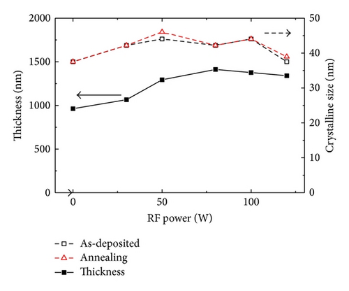
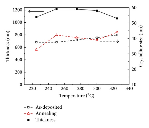
The crystalline sizes of AZO films are 37.5, 42.2, 44.0, 42.2, 44.0, and 37.5 nm for RF power is 0, 30, 50, 80, 100, and 120 W, respectively. The crystalline sizes of the films generally are kept around 43 nm, except when RF is 0 W or 120 W. The crystalline sizes of AZO films are 37.5, 37.5, 39.0, 40.5, and 42.2 nm for the substrate temperature varies from 225, 250, 275, 300, to 325°C, respectively. The crystalline sizes increase with the substrate temperature.
The solid squares in Figure 2(b) give the thickness versus substrate temperature. The deposition rate of AZO film is 0.60, 0.68, 0.68, 0.66, and 0.59 nm for substrate temperature of 225, 250, 275, and 300 and 325°C, respectively. The AZO film has the highest deposition at 250°C substrate temperature and then, decreases with the substrate temperature.
Figure 3(a) gives the in-plane stress for the AZO as deposited at 325°C with various RF power; the stress generally increases with the RF power. Figure 3(b) shows the in-plane stress for the AZO as deposited at 225, 250, 275, 300, and 325°C, respectively. The results of Figure 3 are calculated from (2), where C11 = 208.8 × 10⁹ N/m2, C33 = 213.8 × 10⁹ N/m2, C12 = 119.7 × 10⁹ N/m2, and C13 = 104.2 × 10⁹ N/m2 were used [17–19]. 80 W DC power and 30 W RF power were used during sputtering. The minus sign indicates the compressive stress. The stress generally increases with the RF power and increases to 1.41 × 10⁹ N/m2 from 225 to 250°C substrate temperature and then decreases to 0.40 × 10⁹ N/m2.
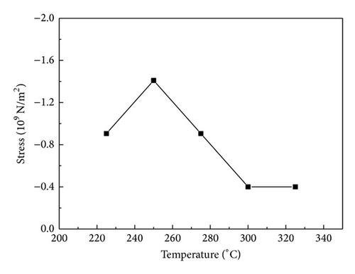
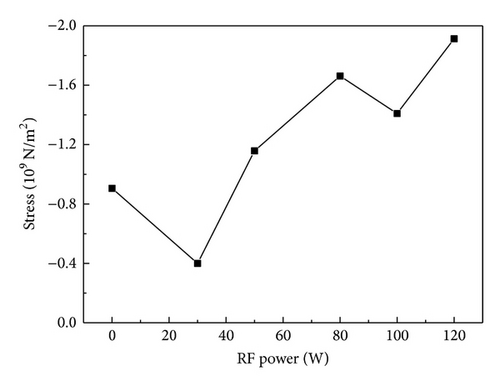
The total film stress contains thermal stress and intrinsic stress. The thermal stress comes from thermal mismatch between AZO thin films and glass substrate. The generation mechanism of the intrinsic stress was caused by the growth process itself. Since the thermal stress is very small, film stress is mainly caused by the growth process itself [18]. Comparing Figures 2 and 3, we conclude that higher deposition rate makes the film stress higher.
3.2. Electrical Characteristics
Figure 4 shows electrical property of the sputtered AZO film versus substrate temperature, where the dash lines indicate the resistivity, solid lines the electron concentration, and the dot lines the electron mobility, respectively. The squares indicate the as-deposited samples and the triangles the annealed samples, respectively.
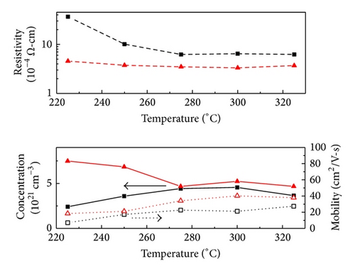
The electron mobility for the annealed samples increases with the substrate temperature and is larger than that of the as-deposited samples, which could be due to the recrystallization of the annealed samples that increases the grain size which increase the electron mobility. The electron concentration of the annealed samples decreases with the increasing substrate temperature. For the as-deposited samples, both electron mobility and electron concentration increase with the increasing substrate temperature. Heating the AZO film, a considerable increase in conductivity was obtained due to the increase in oxygen defects, which increase the electron concentration in the film [9, 10]. In the meantime, the thermal process has the effect of increasing grain size and crystallinity of the film, which results in less grain boundary scattering [6, 9, 10]. These combined actions increase the conductivity. Therefore, the resistivity decreases with the increasing substrate temperature except for the annealed samples, since the resistivity is reciprocal to the product of electron concentration and electron mobility. The resistivity of annealed samples, although decreasing with the increasing substrate temperature, was kept around 3.5–4.5 × 10⁻⁴ Ω-cm. This could be due to the decrease of electron concentration at higher substrate temperature. Hydrogen annealing process introduces the hydrogen into the AZO film, resulting in a shallow donor in AZO film [11].
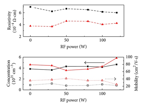
Figure 5 shows electrical property of the sputtered AZO film versus RF power with substrate temperature 325°C, where the dash lines indicate the resistivity, solid lines the electron concentration, and the dot lines the electron mobility, respectively. The squares indicate the as-deposited samples, and the triangles indicate the annealed samples, respectively. The resistivity of the as-deposited samples decreases with the RF power. The electron concentration increases slightly with the incident RF power for the as-deposited samples; however, the mobility of AZO film decreases slightly with the incident RF power.
3.3. Optical Properties
4. Summary and Conclusions
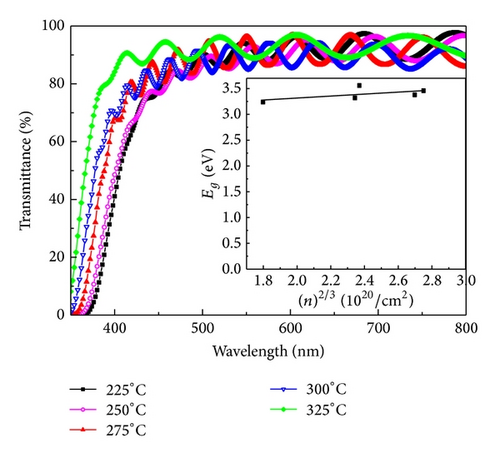
AZO films were deposited by a magnetic control sputtering system using DC power and RF power simultaneously under different sputtering conditions. The AZO films present (002) oriented preference. The deposition rates for RF power = 0 W to 80 W increase from 0.54 nm/s to 0.79 nm/s which are good for mass production. In-plane stress for all AZO films reveals compressive stress. The stress increases with the RF power, increases to 1.41 × 10⁹ N/m2 from 225 to 250°C substrate temperature, and then decreases to 0.40 × 10⁹ N/m2. The transmittance for the film with higher substrate temperature is generally above 80% in the 400 nm~800 nm visible light region. The electron mobility for the annealed samples is larger than that of the as-deposited samples due to the recrystallization of the annealed samples that increase the grain size, resulting in the increasing electron mobility. The lowest resistivity for the annealed samples is 3.5 × 10⁻⁴ Ω-cm which is the best result ever reported by using DC and RF sputtering simultaneously. Furthermore, the sample with higher deposition temperature revealed a significant blue shift phenomenon which may have a great application for electrode in solar cell.
Conflict of Interests
The authors hereby declare that there is no conflict of interests with any financial organization regarding the material discussed in the paper.
Acknowledgment
This work was supported by the National Science Council Taiwan, under Grant NSC100-2221-E-164-004.


