Temperature Effect on the Microstructures and Optical Properties of ZnO Nanowires
Abstract
Temperature effects on the microstructures and optical properties of ZnO nanowires were investigated extensively. Furnace calibration results showed that temperatures inside the tube furnace had Gaussian distribution. Both radial and axial growth rates of ZnO nanowires in the Arrhenius plot fall on straight lines. With the increase of temperatures, ZnO nanowires exhibited larger diameters, better crystal qualities, and preferred growth along 〈0002〉 directions. Enhanced UV emission with the increase of growth temperatures was observed, while green emission was greatly reduced.
1. Introduction
ZnO nanowires (NWs) are receiving increasing interests because of their potential uses in light emitting devices (LEDs), Ultra-violet (UV) lasers, sensors, nanogenerators (NGs), and so forth [1–3]. To fabricate all kinds of ZnO-based nanodevices, controllable synthesis of well-aligned ZnO NWs with desirable lengths, diameters, crystal orientations is a prerequisite step. Although multiple methods have been developed, chemical vapor transport and condensation (CVTC) [4] is generally thought to be the best technique to fabricate defect and impurity-free-single crystalline ZnO NWs. It is very convenient to obtain vertical ZnO NW arrays using CVTC method. However, in CVTC process, ZnO NWs are extremely sensitive to the experimental conditions, such as temperatures, gas flow rates, carrier gas type, Zn vapor rate, environmental humidity, and so forth [5]. Subtle change of the parameters, may lead to totally different morphologies. To study the effect of one condition (i.e., temperature), all the other parameters must be kept absolutely constant. Because of the diversities of the fabricating conditions, systematically studies on how these conditions affect the structural and physical properties of ZnO NWs remain challenging and rarely reported [6, 7]. Temperature is the basic and most important parameter affecting the growth of ZnO NWs. In this work, extensive studies on the temperature effect were carried out.
2. Experimental Description
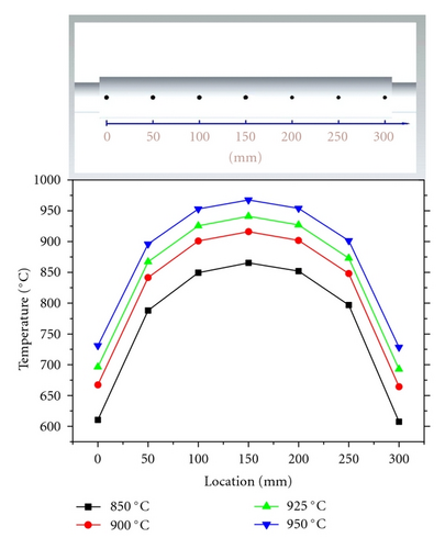
A tube furnace (Lindberg blue) was used to grow ZnO NWs via traditional CVTC method. Before growth, the temperatures of the tube furnace were carefully calibrated using a TES 1310 K type thermometer. 7 points with an interval of 50 mm were set along the tube to monitor the real temperature (Figure 1(a)). During the furnace calibration process, the furnace temperatures were set to 850°C, 900°C, 925°C, and 950°C, respectively. Real temperatures at the 7 points were measured and recorded.
A-plane sapphire single crystals coated with randomly dispersed Au nanoparticles (5 nm) were used as substrates. Equal amounts of ZnO nanopowders (Alfa Aesar, 99.99%) and graphite powders (Alfa Aesar, 200 mesh, 99.9%) served as precursors to produce Zn vapor source. The total weight of the mixed powders was kept constant for each growth cycle to exclude any possible influences. The growth temperatures were set to 850°C, 900°C, 925°C, and 950°C, respectively. Other fabricating parameters are kept constant: Ar flow rate 12 sccm, growth time 10 mins, temperature ramping rate 50°C/mins.
The morphologies of all samples were characterized by scanning electron microscopy (SEM, FEI Quanta FEG). Room temperature photoluminescence (PL) spectra were collected using Flurolog-3-p type spectrometer in the air. The crystal structures and orientations were analyzed using X-ray diffractometry (XRD) (D8 ADVANCE, Bruker AXS).
In order to accurately control the growth temperature of ZnO NWs, the furnace temperatures at different positions must be calibrated first. As is shown in Figure 1(b), the temperatures exhibit Gaussian distributions along the furnace. The center of the tube furnace has the highest temperature (closest to the setting points). Towards two ends of the tube, temperatures decrease gradually. According to the temperature distribution curves, we can know the exact growth temperature of ZnO NWs by monitoring the locations of substrates.
3. Results and Discussions
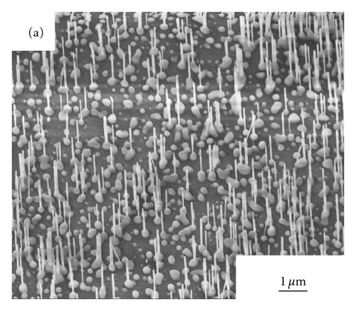
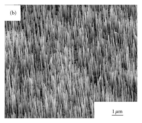
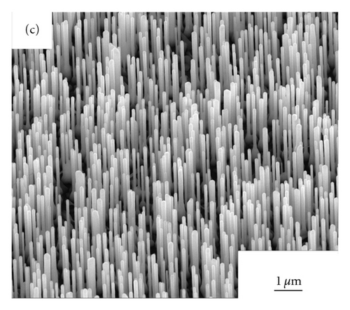
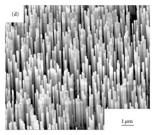
Figures 2(a)–2(d) show the SEM images of ZnO NWs grown under 850°C, 900°C, 925°C, and 950°C. As can be seen from Figure 2, with the increase of heating temperature, the diameters and lengths of NWs are distinctly various, which may be caused by the migration rates of zinc interstitials, and vacancies are largely dependent on growth temperature [8]. At the temperature of 850°C, only sparsely dispersed short and thin nanowires were observed on the sapphire substrate and the average diameters of NWs is 40 nm, with the length of NWs is approximately 0.83 μm. When the growth temperatures of ZnO NWs rose up to 900°C,925°C, and 950°C, dense vertically aligned ZnO NW arrays can be observed. With the increase of temperature, the average diameters of ZnO NWs became 65 nm, 163 nm, and 196 nm respectively, and the average lengths of NWs was 1 μm, 2.1 μm, and 2.9 μm. The increase of the diameters of ZnO NWs must be caused by the Oswald ripening effect of Au nanoparticles when annealing at high temperatures.
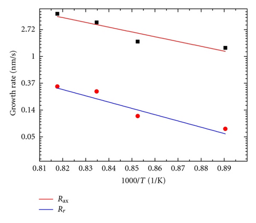
where A is the preexponential coefficient, Ea is the activation energy of the NW growth, R is the gas constant, and T is the absolute temperature. Activation energy in radical and axial direction in growth process of ZnO NWs can be calculated. The activation energy for axial and radial ZnO NW growth is as Eax = 148.42 KJ and Er = 191.63 KJ, respectively.
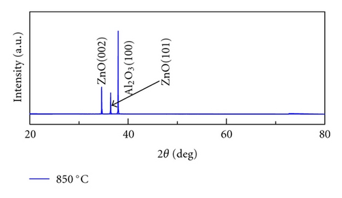
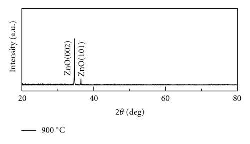
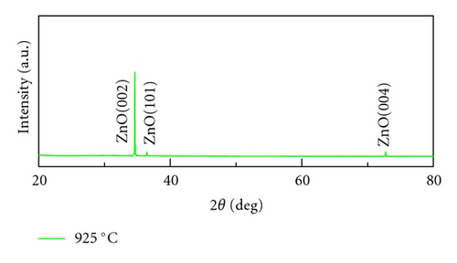
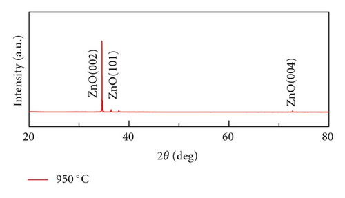
Crystal structures of ZnO NWs fabricated under different temperatures were characterized by XRD using Cu Ka radiation source with the wavelength of 0.154 nm. As is shown in Figure 4, all the ZnO NWs show strong ZnO (002) diffraction peaks, indicative of the basal plane growth mechanism. With the rising of the temperature, the relative intensity ratios of ZnO (002) and ZnO (101) peak also increase. The calculated ratio of I(002) and I(101) is 1.2, 7.5, 18.2, 29.6, respectively, when the growth temperature is 850°C, 900°C, 925°C, and 950°C. It implied that crystal quality of ZnO NWs was improved and c-axis growth is preferred with the increase of heating temperatures. Only Al2O3 (100) diffraction peak was observed when the growth temperature is 850°C due to the low density of NWs, which is corresponding to the SEM images in Figure 2(a).
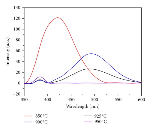
To study the optical properties of ZnO NWs, room temperature PL spectra were tested using He-Cd laser with a wavelength of 325 nm as the excitation light. Figure 5 presents the PL spectra of ZnO NWs fabricated under different temperatures. When the growth temperature is 850°C, only a broad peak centered at 420 nm can be observed, which might be caused by the sapphire substrate. At the growth temperatures of 900°C, 925°C, and 950°C, band-edge emission in the UV region and green emission can be observed. It is appreciable that PL peak intensity in the green region decreases with the increase of the NW growth temperatures. It is generally thought that the green band emission of ZnO NWs is from recombination of photon-generated hole with an electron generated from an ionized oxygen vacancy [9, 10]. Higher growth temperature leads to ZnO NWs with larger diameters, which reduces the surface states and oxygen vacancies and results in the weak green light emission. When the growth temperature is 950°C, the green emission is very weak and only the UV emission centered around 380 nm can be observed, indicating high crystal quality at this growth temperature.
4. Conclusions
In summary, temperature effects on the microstructures and optical properties of ZnO NWs array were studied. By precisely controlling the local temperatures of the tube furnace, NWs were grown under different temperatures through traditional CVTC process. Morphology analysis showed that lengths and diameters of ZnO NWs increase with the rising of temperatures. The growth rates as a function of the reciprocal of temperatures were studied, and the results indicated that the growth of ZnO NWs were in the reaction limited regimes. XRD studies illustrated that higher temperatures could lead to better crystal quality and favor basal growth mechanism. Optical property investigations indicated that higher growth temperature would weak the green light emission, indicative of reduced defects and oxygen vacancies. These results collectively suggest that higher temperatures are preferred to get ZnO NWs with better crystal qualities.
Acknowledgments
This paper is financially supported by NNSF (51072119, 10825209), Shanghai Nano (1052 nm03000,11 nm 0502600), STCSM (10231201103), Innovation Program of Shanghai Municipal Education Commission (12ZZ139), Changjiang Scholar Incentive Program ([2009] 17), and open research program of shanghai key laboratory of modern metallurgy and materials processing.


