The Multi-Field-Coupled Model and Optimization of Absorbing Material′s Position and Size of Electronic Equipments
Abstract
There are three fields in electronic equipment such as structure deformation (S), temperature (T), and electromagnetic (EM) fields. Both deformation and temperature will affect the electromagnetic shielding performance of the equipment considerably, particularly in the case of enclosure with small volume and high packaging density. Because the position of electronic device and the shape of outlet will be changed with structural deformation, there must be therefore an adherent relationship among three fields. To begin with, this paper presents a three-field-coupled model called STEM. Then, to enhance the capability of electromagnetic shielding of the equipment, an efficient way is to attach absorbing material to the inside of it. Under the condition of pregiven material characteristics itself, the position and size of absorbing material are of significant effort on electromagnetic shielding. The optimization model based on STEM is developed in this paper. Next, the numerical and practical experiments of an actual enclosure are given to demonstrate the feasibility and validity of the model and methodology.
1. Introduction
There are two main approaches used in electromagnetic shielding of electronic equipment, reflecting and absorbing. The former makes use of characteristics of good conductor that can reflect electromagnetic wave and restrict the energy in a specific space. However, the energy will not be transformed efficiently. In this case, electronic field of some space is decreased and one of others will be increased. The worst case is led to resonance.
As an efficient way of absorbing shielding, the attachment of absorbing materials is widely utilized. Microwave absorbing material, which is the basic material of modern aerocraft and weapon, support the modern stealthy technique. Since World War II, that had been focused by the defense of each country. At present, absorbing material is used in EMC to simulate semifree and free space in a half-wave and full-wave darkroom. The application is successful [1].
In addition, there are some other areas’ applications, such as eliminating the resonance of cave, reducing interference between circuits, highlighting the stability of circuit, and enhancing the shielding efficiency of enclosure. However, most of researches depended upon engineer experience. Few researches are concerned quantitative application of absorbing material to suppress the electromagnetic interference. In 1988, Dawson and Marvin [2] presented method on restrain of the cave′s resonance by utilizing absorbing material. Henceforth, some scholars [3] are followed.
The shielding doors with big shielding space need to be opened frequently for the purpose of being in and out of people and material. When the shielding doors open, the continuous of electroconductivity is broken, and which leads to the decrease of shielding efficiency. Hence, the dual interlocking shielding doors are adopted in lots of shielding spaces, which can make sure that the electro-conductivity is continuous whenever only one door is opened. This approach keeps the shielding efficiency high, but the effect is poor. Sometimes, the apertures of equipment (such as the feed slot of printers, scanners, and copy machines) are unavoidable, and it is impossible to use the shielding door. For the sake of this, Mauriello [4] submits a purposely study on restraining the electromagnetic leakage with labyrinth and absorbing material by means of model test and numerical simulation.
However, little of the above research considers the optimal position and size of the absorbing material. This paper intends to do it, that is, to search for the optimal value of EMC shielding performance whilst satisfying the constraints of volume, temperature, nonoverlap between the absorbing material by selecting the position and size of materials. This paper will discuss this in detail.
2. The Coupled Model among Electromagnetic, Temperature, and Structural Fields
As shown in Figure 1, under load P1 and P2 and vibration of the base, the chamber will be deformed. As a result, the outlet configuration at the top and front plane will be changed. It further leads to the change of not only boundary of temperature and electromagnetic fields, but also the position of electromagnetic radiate devices (vi and vj) and ventilation window. Besides, the increase of temperature results in decrease of performance of radiate devices. At the right plane, three holes are for the fans to reduce the temperature in the enclosure.
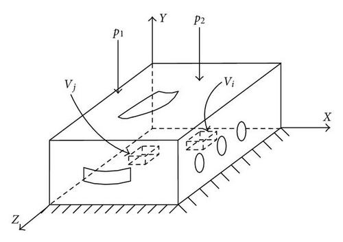
Corresponding to numerical computation of three fields, finite element model of structure is produced at first and the displacement can be known by finite element method, then temperature field and electromagnetic field can be found by finite volume method (FVM) and method of moment (MOM).
- (a)
Establishing the mesh model Γ1 for structural deformation field, model Γ2 for temperature field and Γ3 for electromagnetic field. Generally speaking, the mesh size (for instance, side length of triangular element) in model Γ3 is approximately λ/8, λ is wavelength the mesh size (distance between two node of FVM) in model Γ2 is subjected to Pe ≤ 2, in which Pe = ρuΔx/Γ. Where ρ is fluid density, u fluid speed in x coordinate, Δx distance between two nodes along x-coordinate, andΓdiffusion coefficient.
- (b)
The displacement of structural finite element node can be obtained under the given load. The node position in Γ2 and Γ3 is known from projection matrix.
- (c)
The electromagnetic strength and temperature can be known by MOM and FVM, respectively.
3. Mathematical Description of Optimization Design Problem
As mentioned previously, analysis of electronic equipment refers to electric field (magnetic field) in and out of equipment, temperature distribution in the equipment, and its deformation (when applying external load). Electric field (magnetic field) and temperature distribution will be affected by deformation as the boundary conditions are changed. This paper tries to investigate how the position and size of absorbing material attached in electronic equipment affect the electromagnetic shielding efficiency, under the condition of satisfying temperature distribution requirement.
3.1. Design Variable
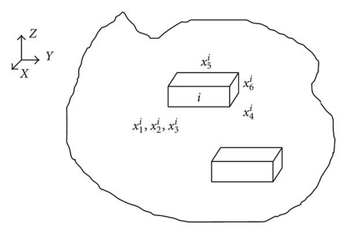
3.2. Objective Function
3.3. Constrained Function
Investigating the above programming problem leads us to the following points. Programming PI is a higher nonlinear programming problem, since the objective and constraint are all higher nonlinear functions of the design variable. Due to the features of electronic equipments and the optimization model, the Hooke-Jeeves method is utilized.
4. Numerical Simulation, Experiment, and Discussion
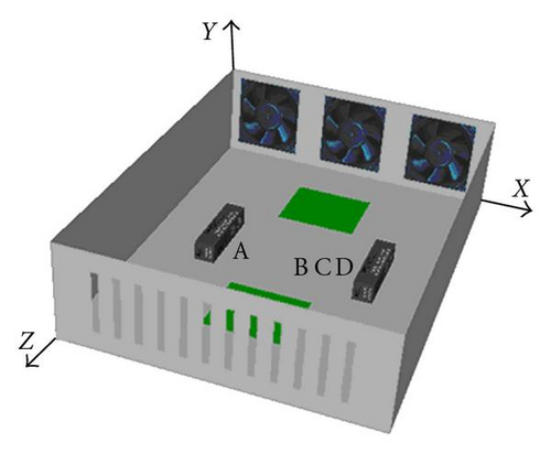
To validate the above model and methodology, an enclosure (Figure 3) is investigated from both of the numerical simulation and practical experiment. They are described as follows.
4.1. Numerical Simulation
The size of the enclosure is 500 × 375 × 125 mm3, the thickness of the wall is 2 mm, the material is aluminum. There are three fans (0.001 m3/s for each) in xoy-plane, evenly distributed along x-coordinate. On the opposite side with z = 500 mm, twelve ventilation slots exist. Each slot is with 100 mm in length and 10 mm in width. The left and right sides of twelve slots are all 50 mm, while the top and bottom side of twelve slots are all 12.5 mm. Two heaters (5 W for each) are fixed on the bottom (Figure 3) with (x, y, z) = (93.75,0, 250) and (281.25,0, 250) mm, respectively. The size of two heaters is 0.03 m, 0.1 m and 0.03 m in x, y and z directions. The material is Nylon-glass filed with conduct heat coefficient 0.214 W/m·K. In addition, there is an electromagnetic radiation module at position (x, y, z) = (187.5, 0,125) mm with the power of 1 w and a sensitive module at the position (x, y, z) = (187.5,0, 375) mm, both modules are treated as probes with the same size as 5 mm high in y-coordinate and all 1 mm in x and z coordinate. The focused frequency ranges from 657 MHz to 803 MHz.
The inlets, where fans located, are shielded by perforated plates whose shielding efficiency is supposed perfect due to the small pore diameter. Therefore, leakage is not considered. The leakage which should be considered is induced by the outlets that composed of twelve ventilation slots.
The discrete models Γ1, Γ2, and Γ3 corresponding to three fields are established. Γ1 for structure is with 1,374 nodes and 2400 triangle elements. Γ2 for electromagnetic field is composed of 1374 nodes, 2,400 metallic triangles and 10 metallic line elements. As for temperature Γ3, there are 280,664 elements and 295,316 nodes.
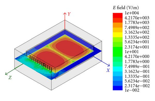
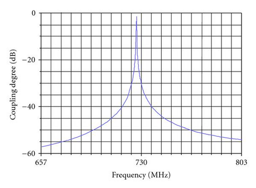
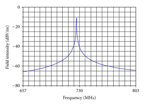
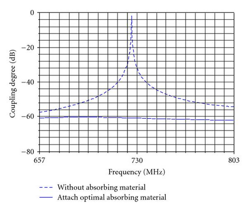
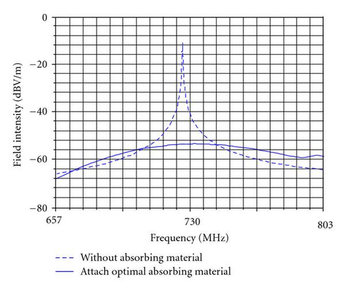
Figure 4 shows that the two positions are at the top of the enclosure where the strongest electric field happened. Thus, attach two pieces of absorbing material of dielectric loss type at these points. The absorbing material is acieration foam, whose thickness is fixed as 50 mm, so two variables of thickness and center position along y-coordinate are fixed. As a result, only four independent design variables for each one are remained (Table 1). Two dimensions along x-coordinate and z-coordinate are not less than 15 mm. In Table 1, and (i = 1,2) are the center and length of the ith absorbing material along x-coordinate. and are the center and length of the ith absorbing material along z-coordinate. Resonance appears at around 730 MHz in the cave, whose mode is TE102, as showed in Figures 5 and 6. When resonance, the coupling degree related to two probes increases rapidly, as well as electromagnetic field intensity leaking from the outlets.
| Design variable |
(mm) |
(mm) |
(mm) |
(mm) |
(mm) |
(mm) |
(mm) |
(mm) |
Cmax (mm) |
Emax (dBV/m) | T °C |
Area m2 |
|---|---|---|---|---|---|---|---|---|---|---|---|---|
| Initial value | 180 | 35 | 117.5 | 35 | 180 | 35 | 367.5 | 35 | −33.3 | −11.6 | 59.69 | 0.0025 |
| Optimal value | 255.0 | 151.3 | 138.5 | 149.6 | 107.5 | 140.0 | 360.8 | 140.4 | −48.7 | −28.3 | 78.24 | 0.04067 |
| Upper limit | 352.5 | 375 | 242.5 | 250 | 352.5 | 375 | 492.5 | 250 | / | / | / | / |
| Lower limit | 7.5 | 15 | 7.5 | 15 | 7.5 | 15 | 257.5 | 15 | / | / | / | / |
Suppose the admissible total volume of absorbing material is 40500 mm2, and the admissible maximum temperature is 95°C. Let α1 = α2 = 0.5. The initial values, upper and lower limits of design variables and the optimal values are given in Table 1. Figures 7–9 show the iteration history of the objective and constraint functions.
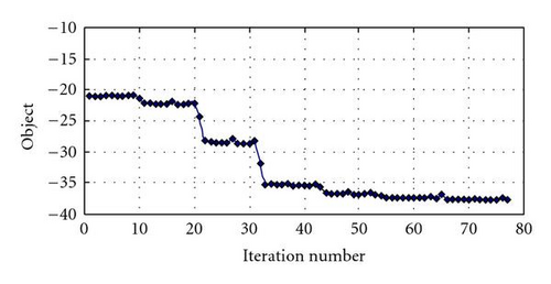
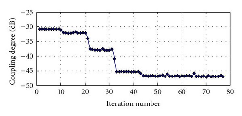
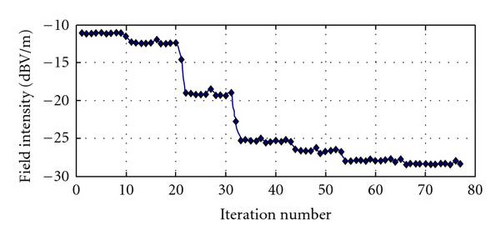
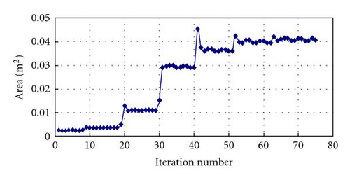
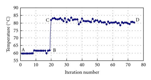
The iteration history of the objective and constraint functions are smooth, and the shielding efficiency became better with the iterations, as shown in Figure 8.
Figure 9 shows that strong relation exists between shielding efficiency and volume of absorbing material. The bigger the volume, the better the efficiency will be in suppressing the electromagnetic resonance. However, too large volume will obstruct the heat transfer. This is a conflict. Tradeoff between them is necessary.
The coupling degree between two probes and field intensity 1 meter away in the cases that there is no absorbing material or two pieces at the optimal positions, respectively, in Figures 10 and 11. It is obvious that both decreased and the efficiency is significant.
5. Concluding Remarks
The experience of theoretical analysis, numerical simulation, and practical experiment may lead us to the following conclusions.
Electromagnetic shielding of complex electronic equipment is actually a multi-field-coupling problem in theory, a new three-filed-coupling model STEM is developed in the paper.
The optimization model of searching for the best shielding performance by selecting the optimal value of the absorbing material’s position and size is submitted based on the model of STEM.
The numerical experiments of equipment are carried out to demonstrate the proposed model and methodology.
It should be noted that the multi-field-coupling problem is a complex and difficult problem. The study about this is still initial, and thorough research needs to be done further.
Acknowledgments
The authors would like to show their special thanks to Dr. F. S. Zhang, B. Y. Ma, N. Han, S.B. Jiang and P. Li for their help of preparing this paper. The paper is supported by National Natural Science Foundation of China with Grant no. 50475171.


