The Influence of Deposition Conditions on Structural Properties of PbI2
Abstract
The effect of deposition environment conditions on the electrical and structural properties of deposited PbI2 layers were studied. The layers were deposited from solution under dark and room light illumination with and without applying magnetic field. XRD, electrical, and photo-electrical properties were measured at room temperature. An increase in the grain size versus the platelet area was noticed.The electrical properties revealed a dependence on deposition conditions. Dark conductivity increases from 1.7 × 10⁻¹⁰ to 5 × 10⁻⁹ (Ωcm)-1 when deposition was carried out in darkness. A gain factor (the ratio between photoconductivity and dark conductivity) of (23) was obtained. The results indicate that the increase in electrical conductivity is mainly due to the plane 001, where the average number of grain boundaries in this plane sharply decreases when deposition takes place in darkness. On the other hand, the increase in photoconductivity could be due to the decrease in the recombination of free carriers along the grain boundaries.
1. Introduction
Lead iodide PbI 2 is a promising compound semiconductor material for X-ray imaging devices [1–4]. It is difficult to grow large crystals of PbI 2 with good uniformity; as a result, they are not well suited for applications such as imaging devices which require large surfaces [5–8]. Using thin polycrystalline layer instead of single crystal wafer is an alternative approach to overcome this difficulty which takes advantage of intrinsic properties of lead iodide [9–12].
Deposition of a layer of PbI 2 polycrystalline from solution is a very comfortable and reliable technique [8–11]; the basic principle requires controlled precipitation on substrate in order to form a layer. Hence, the characterization of electrical and structural properties of such layers is of a great concern both for evaluating their ability to fulfill the requirements needed and for improving their preparation.
Although the application of the external magnetic field during the electrodeposition process has gained a lot of attraction [13, 14], little work is found in the literature on the improvement of the thin film by the application of the external magnetic field during the solution deposition process.
In view of this situation we have investigated the structural and electrical properties dependence of the deposited layer on the deposition conditions (including applying homogeneous external magnetic field, room light illumination, and darkness) in order to understand the transformation accompanying the growth from solution.
2. Sample Preparation
Polycrystalline PbI 2 layers samples were prepared on glass substrates using solution growth by employing PbI 2 powder, prepared in the laboratories without further purification. As checked by X-ray fluorescence, the main residual impurity in the base material is Ag < 4 ppm in weight. The polycrystalline layers were grown by dissolving the powder in deionized water at 100 cc up to the limit of solubility of (4.2 g/L at 100 °C) [6]. Then, the solution was slowly cooled down to 20 °C, and precipitation of small crystallites occurs rapidly. After evaporation of the excess water, thick layers (typically 3–17 μm thick) were obtained on the glass substrates. Two samples undergo precipitation under the influence of magnetic field (0.2 T) parallel to the deposition direction, one under room light illumination, and the second in darkness. In order to determine the influence of the magnetic fields on the properties of the deposits, depositions were carried out under a magnetic field. For electrical measurements two graphite electrodes (parallel strips at 5 mm in width, separated by 5 mm) were deposited on the front surface.
3. Structure Properties
4. Electrical Conductivity
5. Results and Discussions
5.1. Reflection Optical Microscopy
The optical micrographs shown in Figures 1(a)–1(d) reveal that the layers are made of hexagonal platelets parallel to the substrate plane. The sizes vary from few micrometers to tens of micrometers.
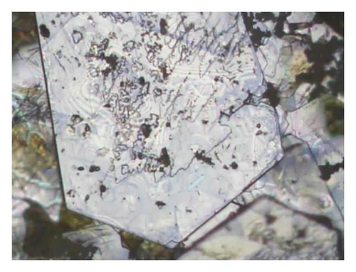
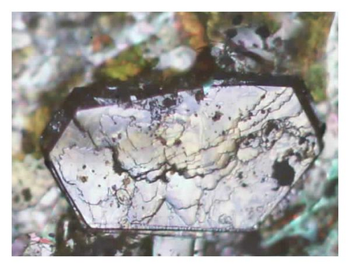
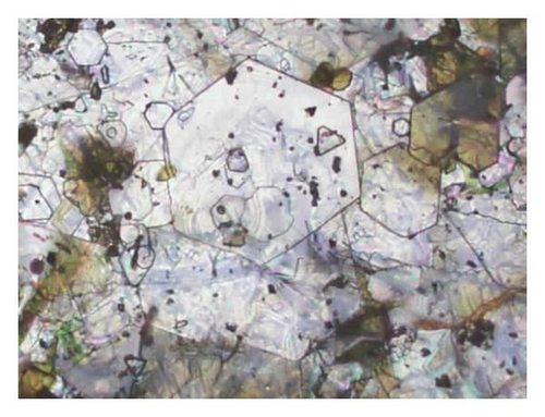
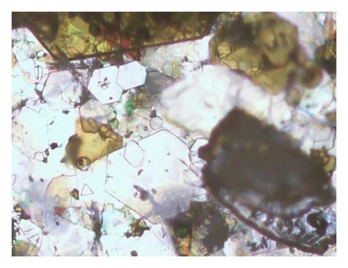
Table 1 summarizes the calculated platelets area in the pictures. It is clear that deposition in dark gives the largest platelets area while deposition in dark with an applied magnetic field decreases the platelets area. Deposition under normal illumination with and without magnetic field gives the smallest platelets area. The results could be explained by adopting the survivor of the fastest model [15]. According to this model nucleation with various orientations can be formed at the initial stage of the deposition and each nucleus competes to grow but only nuclei having the fastest growth rate survive [16]. The decrease of the platelet area with applying magnetic field is probably due to the opposite direction of the magnetic field lines and the direction of the highest growth rate. It seems that lighting and applying magnetic field could block the lateral growth mode.
| samples | Deposition conditions | Average platelets area μm 2 |
|---|---|---|
| 1 | Dark without applied magnetic field | 180.75 |
| 2 | Dark with applied magnetic field | 78.48 |
| 3 | light without applied magnetic field | 23.11 |
| 4 | light with applied magnetic field | 15.584 |
5.2. X-Ray Diffraction Analysis
From the X-ray diffrograms the planes orientations were determined. Besides, grain size, number of layers (NL), and microstress (σs) of PbI 2 were calculated. Figures 2(a)–2(d) shows the XRD of deposited samples prepared under different conditions. Peaks are observed at d = 6.95, 3.489, 2.328, and 1.7447 A ° corresponding to (001), (002), (003), and (004) planes respectively; these results are in good agreement with data achieved by [16, 17], while peaks belonging to (102) and (201) planes mentioned in [18] are missing. The height of the (001) peak decreases with applying magnetic field in both cases. The position of the peaks, that is, the crystallographic orientation of the deposited layer, was not shifted in the four samples during the deposition of the layers. Changing deposition condition caused no additional peaks.
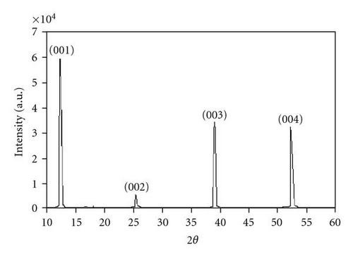
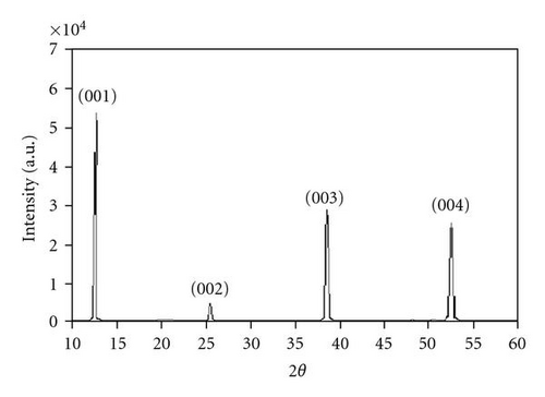
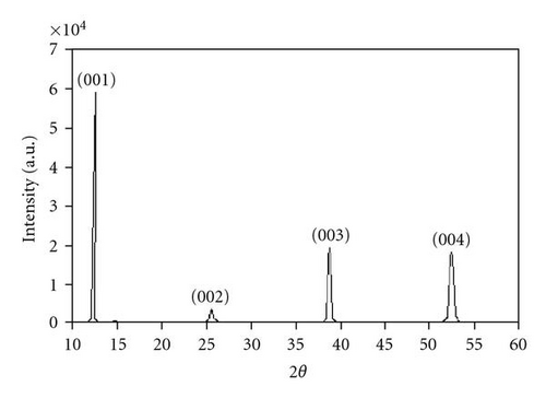
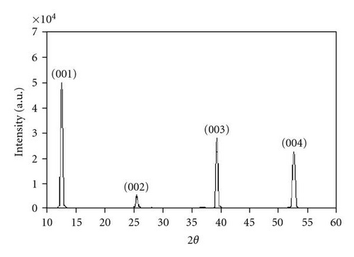
The corresponding data, that is, the interplanar distance, average grain size, number of layers, and microstress are presented in Table 2. The largest grain sizes are those of layers deposited under dark without applying magnetic field. The small grains belong to the sample deposited with light under magnetic field. Decreasing grain size with applying magnetic field was observed during the electrodeposition assisted by applied magnetic fields [19, 20].
| Sample | 2? (degree) | d (A °) | (hkl) | Grain size A ° | NL |
|---|---|---|---|---|---|
| Sample 1 | 12.7159 | 6.95896 | (001) | 682.6201 | 160 |
| 25.5079 | 3.48924 | (002) | 563.7793 | 206 | |
| 38.6427 | 2.32813 | (003) | 474.6347 | 244 | |
| 52.3991 | 1.74474 | (004) | 805.2267 | 144 | |
| Sample 2 | 12.732 | 6.9472 | (001) | 644.573 | 164 |
| 25.4861 | 3.49217 | (002) | 560.3059 | 176 | |
| 38.6385 | 2.32838 | (003) | 390.0919 | 254 | |
| 52.3645 | 1.74581 | (004) | 925.2506 | 107 | |
| Sample 3 | 12.7173 | 6.9552 | (001) | 620.2268 | 161 |
| 25.4451 | 3.4977 | (002) | 542.9319 | 173 | |
| 38.5992 | 2.33066 | (003) | 585.751 | 160 | |
| 52.3258 | 1.74701 | (004) | 1004.105 | 93 | |
| Sample 4 | 12.7157 | 6.95607 | (001) | 501.9222 | 192 |
| 25.5132 | 3.48852 | (002) | 540.2273 | 178 | |
| 38.6713 | 2.32648 | (003) | 531.3026 | 182 | |
| 52.3824 | 1.74526 | (004) | 958.8356 | 100 | |
The number of deposited layers (NL) under light and magnetic field has the higher value, while sample deposited in dark without magnetic field has the smallest value NL.
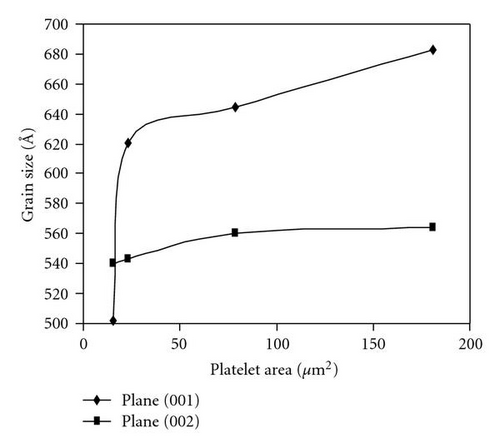
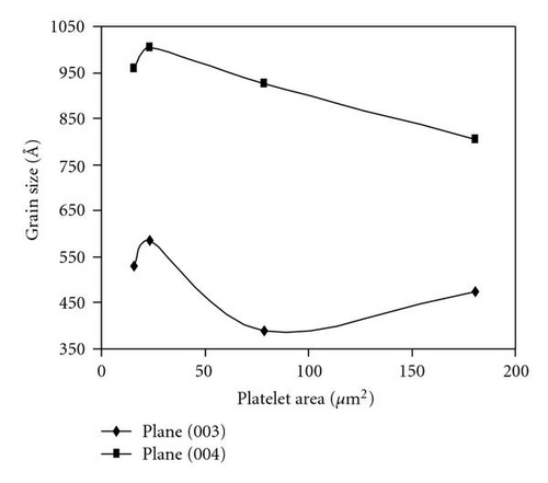
Figures 3(a) and 3(b) show the variation of the grain size with the platelets area for the four growth plans. It is clear that the grain size increases with the increase of platelet area for plane (001) and decreases for (003), (004) plans when the deposition is carried in dark. We think that growth under darkness condition can increase the nucleation frequencies so that nuclei spacing will be small resulting in nuclei growth and coalesce. The principal force behind grain growth is the reduction in the grain boundary surface area per unit volume.
5.3. Electrical Conductivity
Electrical conductivity was calculated from the current-voltage characteristics. Figures 4(a) and 4(b) shows ohmic behavior of both dark and photocurrents for all four samples. By comparing the four curves Figure 4(a) it is concluded that the dark current is higher for the sample deposited in dark with applying magnetic field, while deposition under illumination with and without applying magnetic field gives lower dark current. The low current value for samples deposited under illumination is probably due to the influence of grain boundaries. The grain size was found smaller under illumination; hence the density of their grain boundaries is higher {Figure 3(b)}. This in turn reduces the mobility of charge carriers due to scattering. The influence of grain size is reflected in the photocurrent which in samples (1, 2) is higher than that of samples (3, 4). The increase in the photocurrent is probably due to the reduction of the recombination that takes place in the grain boundaries.
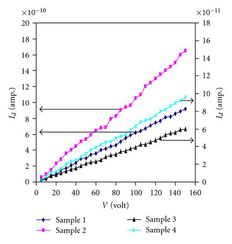
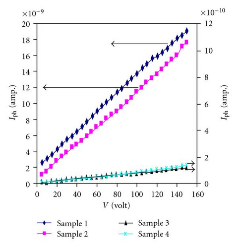
Table 3 shows the variation under dark of the photoconductivity as a function of deposition conditions. The electrical conductivity of samples deposited in darkness is higher than those deposited under light. This could be probably due to the enhancement of the moblities and the reduction in the grain boundary density.

The photoconductivity in PbI 2 layers is due to both direct band-to-band optical transitions and transitions from impurity level (Ag) where both contribute to the creation of electron-hole pairs. The transport of these carriers is determined by the granular structure of the layers and associated trapping centers. Δσ/σd (Δσ = σph − σd) (optical gain) is a measure of the layers response plotted in Figure 6 as a function of the platelet area. The ratio increases monotonically but nonlinearly; the ratio of sample 1 is higher by a factor of (14) than that of the other three samples.

6. Conclusion
It has been shown that polycrystalline lead iodide layers with interesting structural properties can be prepared by means of a simple solution growth methods. The deposited layers are made of hexagonal platelets parallel to the substrata planes. Their sizes differ from a few micrometers to a tens micrometers. All XRD patterns had the same peaks. Neither on the crystal structure nor on the texture, lighting or magnetic field effect has been observed. All layers irrespective of deposition parameters develop a preferred (001) plane. The grain size increases with the increase of the platelets area when deposition is carried out in darkness (682.6201 A ° for platelet area of 180.75 μm 2, 540.2273 A ° for platelet area 15.584 μm 2). The illumination impact on the chemical reaction rates had strong consequences on the resulting layer characteristics. The most pronounced effect is the electrical characteristics. Dark conductivity increases from 1.7*10 −10 to 5*10 −9 (Ωcm)−1 when deposition is carried out under darkness. A gain factor (23) was also attained.


