Multiobjective Optimization Tool for a Free Structure Analog Circuits Design Using Genetic Algorithms and Incorporating Parasitics
Abstract
This paper presents a novel approach for a free structure analog circuit design using genetic algorithms (GAs). A major problem in a free structure circuit is its sensitivity calculations as a polynomial approximation for the design is not available. A further problem is the effect of parasitic elements on the resulting circuit_s performance. In a single design stage, circuits that are produced satisfy a specific frequency response specifications using circuit structures that are unrestricted and with component values that are chosen from a set of preferred values including their parasitic effects. The sensitivity to component variations for the resulting designs is performed using a novel technique and is incorporated in the fitness evaluation function. The extra degrees of freedom resulting form unbounded circuit structures create a huge search space. The application chosen is an RLC ladder filters circuit design.
1. Introduction
Computer-aided design tools for analog circuits consist almost invariably of circuit analysis or simulation packages; no general-purpose analog circuit synthesis tools are available. Conventional numerical optimization techniques can be used to obtain combinations of component values that satisfy a given design specifications. In addition, conventional optimization techniques operate on circuits after having their desired responses approximated by a suitable polynomial, using ideal components with unrestricted values, and only operating on predefined circuit structures. The restrictions introduced by predefining the circuit structure waste extra degrees of freedom in the design process and can conceal many novel design structures that can satisfy the target response and at the same time enhance the design process.
In previous papers [1–5], evolutionary computation algorithms are applied to fixed structure circuit designs to satisfy certain specifications. As mentioned earlier, the predetermination of the circuit structure required in conventional design techniques is a limiting factor when considering a powerful search technique such as genetic algorithm. A few attempts have been made to include structure synthesis in genetically-based optimization techniques such as GA [6, 7] and genetic programming (GP) [8]. However, these techniques suffered huge delays and memory usage and needed to be used in conjunction with circuit analysis packages such as PSPICE [9, 10].
There is still a need, however, for more efficient algorithms that are faster, self-sufficient and can function independently. An efficient measure of performance based on the sensitivity for component variations for the resulting circuits and the incorporation of the parasitic effects associated with components is still needed. This is particularly important in the development of new generations of analog programmable analog arrays (APAAs) programming tools. In this paper, an efficient GA technique for free structure analog circuit design is described. The technique incorporates a sensitivity measure to compare between potential solutions and incorporates parasitic effects.
2. Genetic Algorithms
The field of genetic algorithms [11–13] was founded by Holland in the early 1970s. In [12], Holland emphasizes the ability of simple representations to encode complicated structures and the power of simple transformations to improve that structure. These representations are combined in what is called in biology a chromosome (also referred to as individuals). A number of these chromosomes will constitute a population. Syntactic operations are then used to alter and improve these coded solutions.
The standard genetic algorithms invented by Holland are the basic form from which other improved algorithms have been subsequently developed. As mentioned earlier, the problem to be optimized has to be encoded into a chromosome-like structure in which each gene or set of genes represents a significant parameter towards the desired solution. A population would consist of a prespecified number of these chromosomes.
Starting from an initial randomly-generated population, a selection mechanism is used to identify and select members that exhibit better characteristics. Those selected chromosomes are then acted upon by genetic operators, such as Mutation and Crossover, which are explained in later sections, to reproduce and generate the subsequent generations. The procedure continues until either a time limit is reached or is achieved.
2.1. Crossover Operator
The Crossover operator is considered to be the most important operator in genetic algorithms. It is also a special characteristic of genetic algorithms over many other search techniques that are inspired by the process of biological optimisation.
In nature, Crossover occurs when two parents exchange parts of their corresponding chromosomes. In genetic algorithms, the same idea forms the basis of the Crossover operator, where useful parts of different parent chromosomes should be combined in order to produce an offspring that benefits from the advantageous bit combinations of both parents. Two-point Crossover is an operator that randomly selects two crossover points within a chromosome then interchanges the two parent chromosomes between these points to produce two new offspring.
Consider the following two parents selected for Crossover. The “|” symbols indicate the randomly chosen crossover points:
Parent 1: 110 | 010 | 10.
Parent 2: 001 | 001 | 11.
After interchanging the parent chromosomes between the crossover points, the following offspring are produced:
Offspring 1: 110 | 001 | 10.
Offspring 2: 001 | 010 | 11.
2.2. Mutation
Mutation is a genetic operator that is used to change individual bits in the chromosome at a specified probability. The motivation for using this operator is that it helps to introduce genetic diversity to new generations. While it is desirable in nature to keep the level of mutation low so that an individual produced by the mutation does not differ too much from its ancestor, this is not always the case in applications of genetic algorithms. Chosen mutation rates typically can range from 0.001 to 0.05. Rates beyond these limits are not recommended in most genetic algorithms applications.
3. Implementation
3.1. Chromosome Adaptation and Structure
In [1–3], the predetermination of the circuit structures has helped in reducing the chromosome length. This was achieved by incorporating the order of the chromosome genes into the node connections information. However, in the case of free structure circuit synthesis this technique cannot be used.
In the case of free structure design, the solution space is much larger and the optimization process is composite. It involves the optimization of two different but highly correlated problems; the structure as well as the sizing of a circuit. Hence, all specifications of the electrical circuit including the structure and the sizing of all the components should be included in the chromosome representation.
The specifications of the electrical circuit include the number of components in the circuit, the type of each component, and a list of connections between the components. Circuit components can include a variety of different types of components, including resistors, capacitors, and inductors.
Given the above information, the chromosome for each circuit comprises a number M of groups of equal bit lengths, and an extra group of bits representing the number of nodes in the circuit; see Figure 1.
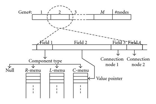
Each gene in the chromosome specifies a component and contains four fields (i) type of component (L, C, etc.), (ii) a pointer to a menu containing component value, (iii) and (iv) circuit nodes to which the component is connected; see Figure 1. Two-point crossover rate of 100% and a mutation rate of 0.5% were used for the GA operators.
It is generally desirable for a low-cost design to use the least number of components. For this reason a Null component, representing an open circuit, is introduced into the component type menu.
3.2. The Design Program
On entry the user is required to supply the following input data.
Type of filter (low pass, high pass, band pass)
- (i)
ω1, αmin.
- (ii)
ω2, αmax.
- (iii)
N, the maximum number of nodes. Optional and can be used to limit the search to a certain number of designs.
- (iv)
M, the maximum number of components (optional).
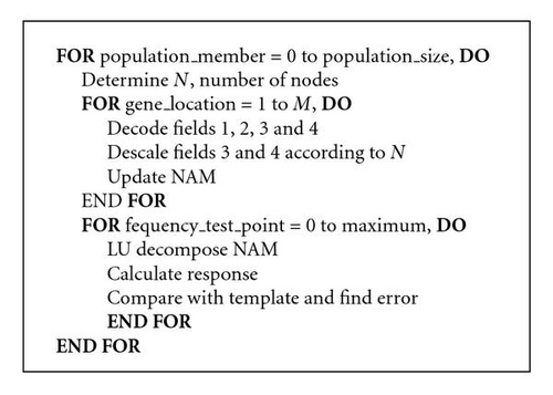
Upon determining type, value and connection nodes, the component value is inserted in the corresponding nodal admittance matrix (NAM) location [14]. When all elements are decoded, contents of the resulting entries in NAM are passed to the calculation function, in which lower-upper (LU) decomposition and solutions to the matrix equations are solved. Figure 2 shows a pseudocode for the program.
4. Least-Squared Error Evaluation
4.1. Specified Weighted Errors
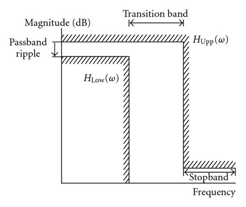
Although the passband will be characterized by a specific passband ripple, the upper boundary of the response represents the maximum power transfer level, the claimed results of LC filter theory. Therefore, testing only the suitability of the lower limit of the response would be sufficient, as the upper limit will never be exceeded in the passband.
In the stopband region, only the upper limit of the specified attenuation level needs to be considered, since any lower value of attenuation meets the specifications. The transition region is considered as a “do not care” region. Thus, it is sufficient to test just the passband and the stopband for confirmations. The different frequency band boundaries are shown in Figure 3. The fitness is taken as the reciprocal of the error function.
4.2. Performance Improvements by Controlling Connection Fields
The number of nodes comprising the circuit is determined at the beginning of the decoding process to control the connection node numbers of the circuit components.
The fields determining the connection nodes are decoded in a way to produce node numbers within N. This is achieved by linear-scaling down the whole range of values of allowed node numbers to only that of N. This helps to avoid circuit structures that would have components connected to nodes that do not exist in the defined structure and which are hence unacceptable and would be a total waste of time to evaluate.
5. Sensitivity Comparison
In [5], the author has developed a rapid feasible region estimation technique using GA. The technique is modified to provide a measure of comparison among the resulting circuit designs using the free structure GA technique described in the previous sections.
6. Extension to Include Parasitic Effects
Parasitics can include wire and wounding resistances and inductors in lumped circuit components as well interlayer capacitances and node to ground voltages. It can also include resistances associated with polysilicon and doped semiconductor regions when used as conductors, and capacitances associated with any crossover, from any conductor to substrate, and with any depletion region in a reverse-biased pn junction, in integrated circuits. Careful layout design can eliminate some of these parasitics, but avoiding them all together is not feasible. Other factors which can also affect the amount of parasitics are the area of the circuit and the packaging density of the chip [15].
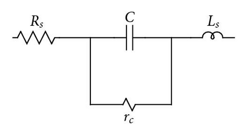
Parasitics can cause significant deviations in circuit performance and should be accounted for in early stages of the design, if their effects are to be minimized. In this chapter, GAs, as described earlier, are modified to include some additional information the designer might want to consider for each circuit component. Parasitic effects considered in this paper include inductor resistance as shown in Figure 4, and series and parallel resistances, and series inductance associated with a capacitor as shown in Figure 5.

To implement the parasitic effects into the circuit design optimisation problem using the GA, an additional parameter is added into the component menu and this represents the parasitic effect of the associated component and the quality factor Q; see Figure 6.


This method will avoid adding to the complexity of the structure and will make it possible to add or remove any effect from the component menu without having to alter the chromosome structure.
In the implementation considered in this work, arbitrary loss factors for components are assumed. The technique is based on the idea to perturb the element values of the lossy filter with the aim of making the magnitude function of the lossy filter proportional to that of the ideal filter at some discrete frequencies in the passband and the stopband. There is no restriction on the Q′s of the elements, provided that they are high enough, and the elements need not have identical Q′s.
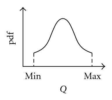
However, the methods outlined need preknowledge of the values of the Q′s for each element, which might not be feasible in practical situation, where designers quite commonly depend on statistical distribution data for their Q values. It is still feasible to specify classes of Q′s, for example, low, medium, and high; but these will reflect a band of randomly distributed values for each class rather than specific values.
It is very likely that the designer will decide on what class of Q′s is needed for a circuit design rather than specific Q values. For this reason, the method used in this work assumes a random distribution of Q values within each class of Q′s; see Figure 6.
6.1. Incorporation of Parasitic Effects in Circuit Designs
In implementing the parasitic effects into the circuit design optimisation problem using the GA, two methods can be applied. The first is to include whatever effects required to be considered in the chromosome structure itself; see Figure 7.
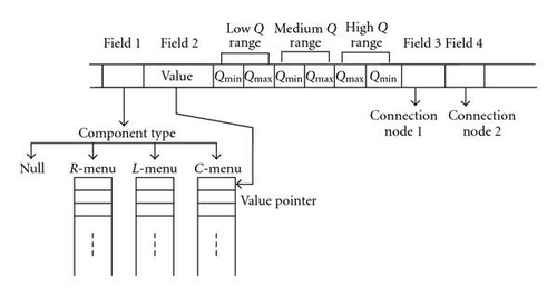
This has the following limitations, firstly it will add to the complexity of the gene structure and the GA operation. This will eventually put limits on the number of additional effects a designer might be able to consider. In addition to that, inserting or removing an effect will require a change in the chromosome structure. Last but not least, effects considered for each type of elements are different and hence different gene lengths will be required to represent each type of elements.
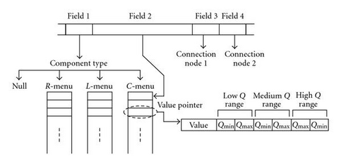
The second method to represent any parasitics into the GA implementation is to associate these effects within the menu listings of elements. Additional effects can then be introduced and any further calculations of these effects can then be made, for example, loss factors; see Figure 8. This method will avoid adding to the complexity of the chromosome structure and will make it possible to add or remove any effect from the component menu without having to alter the chromosome structure.
7. Results
The GA used has a crossover rate of 100% and a mutation rate of 5% throughout all runs. The GA was allowed to run for one thousand generation in each run. However, convergence was reached after an average of one hundred and fifty generations. Each generation had fifty chromosomes or individuals. Each generation took 10 seconds on average in processing. In these implementations, the desired design template is the starting point of the design process, whereas in conventional designs polynomial approximation for the desired response is used [15]. This has the limitation of constraining the feasible solution to sets of design parameters that would satisfy the polynomial approximation. By designing directly from the template specifications, a designer would avoid extra degree of approximation a polynomial fitting would introduce. At the same time, it provides an extra degree of freedom which would enlarge the solution space considerably to include any design that would reside within the design template without necessarily being represented by a polynomial. Also the GA search starts from an arbitrary point in the solution space and needs not to have any prior knowledge of the feasible region of the required design.
7.1. Low-Pass Design
Different low-pass design specifications were considered. One had a passband ripple of 1 dB, minimum attenuation of −100 dB at a transition ration of 10. An average group of five solutions emerged; the frequency response of one of these solutions is plotted in Figure 9. The circuit constructed by the GA is shown in Figure 10. It is noticed that well-known π and T ladder structures have also been generated by the GA. A different design specification of 0.5 dB passband ripple and −60 dB stopband attenuation was tested. Figure 11 shows the resulting circuit design.
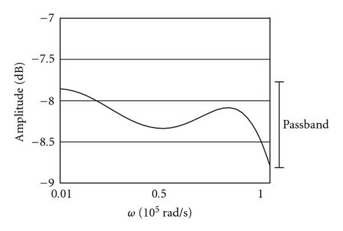
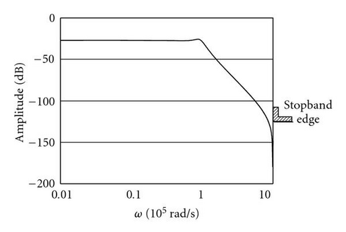
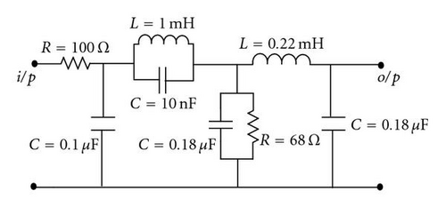
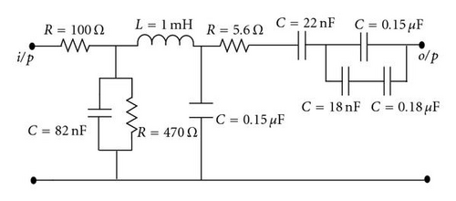
In a different run, two circuits that were designed to meet achieve a maximum attenuation of 1 dB in the passband and a minimum attenuation of −100 dB in the stopband; see Figure 12, Table 1. A comparison between the two circuits was conducted based on the tolerance rage to changes in component values. Figure 9 shows the two circuits used to test the GA program.
| Circuit 1 | Range | ||||
|---|---|---|---|---|---|
| Component | Actual value | Nodes 1 | Nodes 2 | Low | High |
| C1 | 1.80 | 3 | 3 | 1.28 | 2.28 |
| C2 | 2.20 | 2 | 2 | 2.2 | 2.72 |
| C3 | 2.20 | 1 | 1 | 2.2 | 2.72 |
| L1 | 2.20 | 1 | 2 | 1.68 | 2.65 |
| L4 | 1.00 | 2 | 3 | 0.98 | 2.72 |
| L3 | 1.00 | 2 | 1 | 0.5 | 1.09 |
| C5 | 2.70 | 2 | 2 | 2.7 | 3.22 |
| R1 | 1.00 | 3 | 3 | 0.48 | 1.4 |
| L2 | 2.20 | 3 | 2 | 1 | 2.52 |
| C6 | 1.00 | 3 | 3 | 0.48 | 1.48 |
| Circuit 2 | Range | ||||
|---|---|---|---|---|---|
| Component | Actual value | Nodes 1 | Nodes 2 | Low | High |
| L4 | 1.00 | 3 | 2 | 2.2 | 2.27 |
| R1 | 0.10 | 3 | 3 | 0.1 | 0.62 |
| C2 | 1.80 | 2 | 2 | 1.8 | 2.32 |
| C1 | 1.20 | 3 | 3 | 0.77 | 1.57 |
| C3 | 2.20 | 1 | 1 | 1.68 | 2.44 |
| L2 | 2.20 | 2 | 3 | 0.57 | 2.36 |
| L1 | 4.70 | 1 | 2 | 4.7 | 5.22 |
| R2 | 0.15 | 3 | 3 | 0.15 | 0.67 |
| L3 | 1.00 | 1 | 2 | 0.62 | 1.23 |
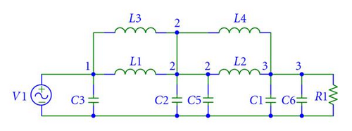
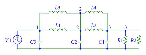
Even though the two circuits have a very close components values, the range generated by the GA program was different. The differences in ranges for each component in the circuits are shown in Table 2. We also note that C2 and C5 in circuit (a) are in parallel, which is equivalent to C2 in circuit (b).
| Circuit b | Circuit a | ||||||
|---|---|---|---|---|---|---|---|
| Component | Range | Difference | Component | Range | Difference | ||
| L4 | 2.20 | 2.27 | 0.07 | L4 | 2.20 | 2.72 | 0.52 |
| R1∥R2 | 0.06 | 0.32 | 0.26 | R1 | 0.48 | 1.40 | 0.92 |
| C2 | 1.8 | 2.32 | 0.52 | C2∥C5 | 1.20 | 1.47 | 0.27 |
| C1 | 0.77 | 1.57 | 0.80 | C1∥C6 | 0.35 | 0.89 | 0.54 |
| C3 | 1.68 | 2.44 | 0.76 | C3 | 2.20 | 2.72 | 0.52 |
| L2 | 0.57 | 1.36 | 0.79 | L2 | 1.00 | 1.52 | 0.52 |
| L1 | 4.70 | 5.22 | 0.52 | L1 | 1.68 | 2.65 | 0.97 |
| L3 | 0.62 | 1.23 | 0.61 | L3 | 0.50 | 1.09 | 0.59 |
| Average difference | 0.54 | Average difference | 0.61 | ||||
As shown in Table 2, the two circuits vary with the difference at some components, but in general, circuit (a) has a higher tolerance range for its component values than circuit (b). This gives circuit (a) fitness leads over circuit (b).
7.2. High-Pass Design
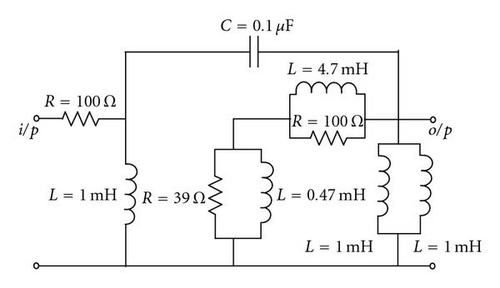
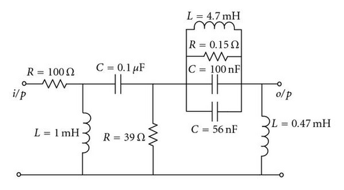
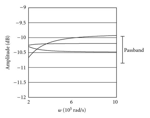
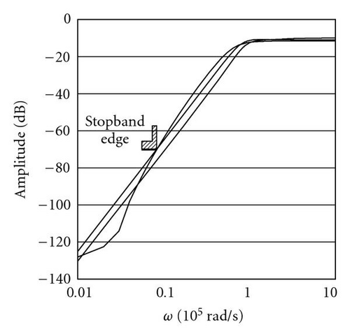
The high-pass filter design is done directly without having to use a low-pass prototype and then performs frequency transformations. A design template of 1 dB passband ripple and attenuation of −60 dB at the stopband edge with a transition ratio of 10 is considered. A number of four solutions on average emerged two of these circuits are shown in Figure 13. The frequency responses of the resulting circuits are shown in Figure 14.
8. Conclusion
This paper has presented a novel circuit design tool by using the GA strong search abilities in both the structure and sizing domains of a circuit design problem. A successful design of the chromosome structure has been obtained to include the full circuit specifications. A novel technique to compare circuit sensitivities to changes in component values among different circuit structures was developed.
It is noticed that well-known π and T ladder structures have also been generated by the GA. That is due to the low sensitivity such structures have, to small changes in component values. This feature was detected by the GA as a result of the sensitivity comparison technique developed in this paper.
So far, the technique described in this paper is limited either passive circuits, or active circuits that are based on passive models. A further extension to include active circuits and three terminal components is underway and will appear shortly in another paper.


