Pre-Fabrication Gettering and Hydrogenation Treatments for Silicon Heterojunction Solar Cells: A Possible Path to >700 mV Open-Circuit Voltages Using Low-Lifetime Commercial-Grade p-Type Czochralski Silicon
Abstract
Pre-fabrication gettering and bulk hydrogenation processes are applied to low-bulk-lifetime (25 μs) p-type Czochralski silicon wafers before silicon heterojunction (SHJ) solar cell fabrication, resulting in effective minority carrier lifetime enhancements by a factor of six. On complete SHJ solar cells, this translates to an improvement in the open-circuit voltage (VOC) of 71 mV, resulting in VOC values as high as 692 mV. This remarkably high VOC suggests that efficiencies approaching 25% could be possible for low-cost p-type Czochralski silicon wafers – not the typical expensive, high-quality n-type ones with lifetimes of several milliseconds – in the near future. This method is also likely applicable to n-type SHJ solar cells to reduce the incoming wafer lifetime requirements and to other silicon solar cell structures featuring passivated contacts.
Hydrogenated amorphous silicon (a-Si:H) thin films provide excellent surface passivation of crystalline silicon wafers.1 This has enabled open-circuit voltages (VOC) of 750 mV in silicon heterojunction (SHJ) solar cells2 and resulted in multiple world-record efficiencies of over 25%,3, 4 with a current record of more than 26.6% using an interdigitated back-contact structure.4 One attributed strength of the SHJ technology is the ability to fabricate cells at temperatures below 250 °C to reduce processing costs and avoid “poisoning” the silicon bulk during high-temperature processes.5, 6 However, the exclusive use of low processing temperatures – which is required because of the loss of hydrogen from the a-Si:H films at higher temperatures – eliminates the possibility of improving the quality of the silicon bulk throughout the cell fabrication sequence with gettering and hydrogenation. This is primarily due to the low diffusion coefficients of impurities including hydrogen and iron at such temperatures.7, 8 As a result, to take full advantage of the excellent surface passivation offered by SHJ structures, high-quality n-type Czochralski (Cz), or float-zone silicon wafers with millisecond starting lifetimes are required to make high-efficiency solar cells.7 This strict wafer-lifetime requirement increases the solar cell production cost and limits SHJ cells to premium markets.
To broaden the application of SHJ structures and reduce the high materials cost of n-type silicon wafers, p-type Cz silicon wafers could be used. In fact, p-type Cz wafers can have bulk lifetimes of over 1 ms9 and can be used to fabricate solar cells with VOCs of up to 730 mV.10 However, the commercial-grade p-type Cz wafers used for mass production of aluminium back-surface field (Al-BSF) and passivated emitter and rear cell (PERC) structures often have much lower lifetimes (below 200 µs), which lead to substantially lower VOC and efficiency values than those of their n-type counterparts. Despite these poor lifetimes, cells fabricated from these wafers have demonstrated VOCs of approximately 686 mV and record efficiencies of 22.7% using the PERC cell technology.11 This high performance is mostly due to the incorporation of gettering and bulk hydrogenation throughout the PERC fabrication process, which are essential for p-type silicon.8 Gettering can reduce the concentration of highly mobile transition metals in the silicon bulk. For silicon solar cells, gettering of detrimental iron is commonly achieved during phosphorus emitter diffusion by segregation to the heavily doped phosphorus regions.12 Hydrogen passivation can electrically neutralize the recombination activity of a range of defects in silicon such as structural and impurity-related defects.13 For silicon solar cells, the introduction of hydrogen into the bulk silicon material is achieved through the deposition of hydrogenated silicon nitride (SiNx:H) as an antireflection coating coupled with the fast firing process for metal contact formation. Hydrogen can also enable a rapid passivation of carrier-induced boron-oxygen defects using a subsequent advanced hydrogenation process with illumination.14
In this study, we demonstrate the impact and importance of pre-fabrication gettering and bulk hydrogenation on the performance of SHJ solar cells using commercial-grade p-type Cz silicon wafers.
Experimental Section: Lifetime test structures and solar cells were fabricated on sistering commercial-grade p-type silicon Cz wafers with a bulk resistivity of 1.6 ± 0.2 Ω cm. Wafers were saw-damage etched in a KOH solution and divided into four primary processing groups: (Control) no pre-fabrication gettering or hydrogenation; (G) pre-fabrication gettering only; (H) pre-fabrication hydrogenation only; and (G+H) pre-fabrication gettering and hydrogenation. Substrates in groups G and G+H underwent RCA cleaning followed by a POCl3 diffusion,8 resulting in a heavily doped n+-emitter layer on both sides with a sheet resistance (Rsheet) of approximately 35 Ω sq−1. A short dip in 2% HF for 2 min was used to remove the phosphosilicate glass. Subsequently, wafers in all groups were alkaline textured to remove approximately 10 μm from each surface – including the diffused emitters – to arrive at a final wafer thickness of 180 ± 3 μm. All wafers then had similar surface characteristics and thicknesses.
In preparation for the pre-fabrication hydrogenation treatment, wafers in groups H and G+H first underwent RCA cleaning. A 75-nm-thick layer of SiNx:H with a refractive index of 2.1 was deposited on both surfaces using a Roth & Rau MAiA plasma-enhanced chemical vapor deposition (PECVD) system. The introduction of hydrogen into the silicon bulk was then initiated using an industrial Schmid fast-firing metallization belt furnace, with a peak wafer temperature of 740 ± 6 °C (Q18 Datapaq) and a belt speed of 4.5 m s−1. The samples were then dipped in 49% HF until hydrophobic to remove the SiNx:H layers.
Before the a-Si:H depositions, wafers were cleaned in solutions of H2O2/H2SO4 and H2O2/HCl and then dipped in buffered oxide etch. Intrinsic a-Si:H(i) films were deposited with a mixture of silane and hydrogen, whereas boron-doped a-Si:H(p) and phosphorus-doped a-Si:H(n) films were deposited by adding an additional doping gas of trimethylboron or phosphine, respectively. 6-nm-thick a-Si:H(i) and 11-nm-thick a-Si:H(p) films were first deposited on the rear of the wafers, and 6-nm-thick a-Si:H(i) and 5-nm-thick a-Si:H(n) films were then deposited on the front using an Applied Materials P-5000 multi-chamber PECVD tool. Note that an in-situ, 30-second-long hydrogen plasma treatment15, 16 was performed immediately after a-Si:H(i) film deposition (on both sides) to improve the a-Si:H(i)/c-Si interface passivation. After a-Si:H deposition, some samples were set aside for lifetime characterization. For the remaining samples, a 75-nm-thick indium tin oxide (ITO) layer was deposited on the front, and a 150-nm-thick ITO layer and a silver electrode were deposited on the rear using direct current magnetron sputtering. Four solar cells, each 2 cm × 2 cm in size, were defined on each wafer by using a shadow mask during the ITO and silver sputtering process. A front silver grid was screen-printed using a low-temperature silver paste, which was subsequently cured at 200 °C for 20 min. Cells were then laser isolated from the larger substrate using a 1064 nm Nd:YAG laser.
Injection-dependant lifetime measurements were carried out on lifetime structures using a quasi-steady-state photoconductance (QSSPC)17 tool (Sinton Instruments, WCT-120) with analysis performed using the generalized mode.18 Effective minority carrier lifetimes (τeff) were extracted at an injection level of Δn = 1 × 1015 cm−3 (approximately equal to 0.1 times the background dopant concentration). The 1-sun implied open-circuit voltage (iVOC) was extracted from the lifetime data.
Cell current density-voltage (J–V) measurements were carried out under standard conditions of 0.1 W cm−2, 25 °C with an AM1.5G spectrum. External quantum efficiency (EQE) spectra were measured using a PV Measurements QEX10 tool. The AM1.5G-weighted integrated EQE curve was used to calculate the active-area short-circuit current density (JSC) and efficiency (η) of devices. Suns-VOC measurements (WCT-120, Sinton Instruments) were performed to evaluate the pseudo fill factors (pFF) of finished devices. In parallel, standard solar cells with a full-area Al-BSF were fabricated on sistering wafers. Processing details can be found in.14
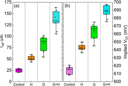
For SHJ solar cell precursors with only a-Si:H layers, the addition of pre-fabrication gettering and bulk hydrogenation processes before SHJ processing had a profound impact on τeff and iVOC (see Figure 1). The control samples with no prior processing reveal the initial wafer lifetimes of only 25 μs, whereas groups G and H demonstrated τeff values of approximately 50 and 75–100 μs, respectively. However, the most significant improvement was achieved using both gettering and hydrogenation, with τeff values of 125–150 μs. The total dark saturation current density (J0) of all samples was 0.5–3.5 fA cm−2, and hence the τeff was limited by bulk recombination. The results highlight the complementary nature of gettering and hydrogenation for attacking orthogonal defects and hence the importance of using both methods to increase the bulk lifetime of p-type silicon wafers, in agreement with previous studies.8, 19 The corresponding improvement in the average iVOC was from 615 mV on the control samples to an impressive 689 mV on samples with gettering and hydrogenation.

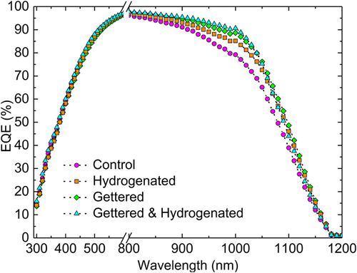
The lifetime enhancements translated to significant improvements in the electrical performance of finished solar cells. Table 1 shows the performance of conventional Al-BSF solar cells, as well as SHJ solar cells with and without gettering and bulk hydrogenation. The control SHJ solar cells had extremely poor electrical parameters with an average VOC of only 621 mV. This value is even lower than that of the relatively low-efficiency Al-BSF solar cell structure with a VOC of 643 mV, which is higher most likely because of natural gettering and bulk hydrogenation that occurs during Al-BSF solar cell fabrication. This VOC highlights the incompatibility of conventional SHJ solar cell processing with low-lifetime silicon wafers. However, with the addition of gettering and hydrogenation before SHJ fabrication, the VOC increased by more than 70 mV, to 692 mV, higher than that of current state-of-the-art PERC solar cells.20 This improvement corresponded to an average efficiency enhancement of 2.7% absolute. EQE measurements indicated a significant increase in the long-wavelength response of the devices through the incorporation of both gettering and hydrogenation (see Figure 2). This increase is consistent with the expectations of increasing lifetime in a front-junction device structure with an improvement in minority carrier diffusion length from 25 to 85 μm – approximately half the thickness of the wafers.
| Group | JSC (mA cm−2) | VOC (mV) | FF (%) | pFF (%) | η (%) |
|---|---|---|---|---|---|
| Al-BSF screen print | 37.0 | 643 | 79.5 | – | 18.9 |
| Control | 38.0 | 621 | 68.9 | 80.2 | 16.3 |
| Hydrogenated | 39.2 | 628 | 66.4 | 74.6 | 16.4 |
| Gettered | 38.8 | 643 | 68.9 | 79.6 | 17.2 |
| Gettered + Hydrogenated | 39.3 | 692 | 69.6 | 78.3 | 18.9 |

To our knowledge, the VOC of 692 mV achieved in this work is the second highest ever reported for a p-type Cz silicon solar cell and equal to that reported by Descoeudres et al.21 The only higher value we are aware of was 729 mV reported by Bätzner et al.10 However, in the studies by Bätzner et al. and Descoeudres et al. no high temperature gettering or hydrogenation was performed and hence it is unclear on the initial wafer quality used. From the low lifetime and I–V results obtained on the low-lifetime material in this work without gettering and hydrogenation, it would suggest that wafers with substantially higher lifetimes were used in those studies.
Impressively, the 692 mV VOC achieved in this work is approaching that of the 25%-efficiency world-record p-type Passivated Emitter, Rear Locally diffused (PERL) cell (706 mV) fabricated using an expensive, high-lifetime float-zone silicon wafer.22 This VOC thus suggests that p-type Cz silicon wafers of modest quality could be capable of efficiencies approaching 25% in the near future. However, with the SHJ processing performed in the vicinity of 200 °C in the dark, the lifetime and I–V results represent values in a non-degraded state prior to the formation of boron-oxygen defects. The use of advanced hydrogenation processes23 to eliminate potential light-induced degradation in the p-type SHJ solar cells will be investigated in a future study.
Pre-fabrication gettering and bulk hydrogenation of SHJ solar cells was investigated using commercial-grade p-type Cz wafers with initial lifetimes of 25 µs. Without extra processes to boost bulk lifetime, a VOC of only 621 mV was achieved, substantially lower than that of conventional Al-BSF cells that naturally receive the benefits of gettering and bulk hydrogenation throughout cell fabrication. However, pre-fabrication gettering and hydrogenation dramatically increased the effective lifetimes of SHJ test structures to 125–150 µs by reducing defect and impurity densities within the wafers. On finished cells this translated to VOC enhancements of >70 mV, resulting in a VOC as high as 692 mV, the highest value reported for low-quality p-type Cz silicon material.
The results clearly highlight the incompatibility of conventional SHJ solar cell processing sequences with low-lifetime silicon wafers, and that this limitation can be overcome using processes before SHJ cell fabrication that typically occur during fabrication of p-type diffused-junction solar cells. These pre-fabrication gettering and hydrogenation processes could relax the initial wafer-quality requirements for high-efficiency SHJ solar cells imposed by the exclusive use of low-temperature fabrication processes. In particular, they could avoid broadening the applicability of the SHJ technology from high-lifetime n-type Cz silicon wafers only to include low-cost p-type Cz or even multi-crystalline silicon wafers. At the same time, gettering and hydrogenation could pave the way for significant efficiency enhancements for p-type solar cells by improving the bulk lifetime to a level at which the wafers can take advantage of the superior surface passivation provided by SHJ structures.
Pre-fabrication gettering and bulk hydrogenation processes could also be beneficial for n-type SHJ solar cells given that high-efficiency homojunction n-type technologies have also benefited from gettering and bulk hydrogenation.24-26 It is likely that high-efficiency solar cell technologies with emerging passivated contact schemes based on metal oxides, alkali metal fluorides and doped polysilicon contacts with tunnelling oxides,27, 28 many which also have strict temperature limitations like a-Si, could also benefit from the addition of these defect engineering methods.
Acknowledgments
B. H., D. C., and J. S.contributed equally to this work. This work has been supported by the Australian Government through the Australian Center for Advanced Photovoltaics (ACAP) and the Australian Renewable Energy Agency (ARENA) (1-SRI001), as well as by the Engineering Research Center Program of the National Science Foundation and the Department of Energy under NSF Cooperative Agreement No. EEC-1041895. Brett Hallam would like to acknowledge the support of the Australian Research Council (ARC) through a Discovery Early Career Researcher Award (DE170100620). The views expressed herein are not necessarily the views of the Australian Government, and the Australian Government does not accept responsibility for any information or advice contained herein. The authors also acknowledge the UK Institution of Engineering and Technology (IET) for their funding support for this work through the A.F. Harvey Engineering Prize. The authors would also like acknowledge measurements performed by Bruno Stefani and Moonyong Kim, and solar cell fabrication and measurement assisted by Zhengshan (Jason) Yu and Ashling Leilaeioun.
Conflict of Interest
The authors declare no conflict of interest.


