Engineering Domain Variants in 0.7Pb(Mg1/3Nb2/3)−0.3PbTiO3 Single Crystals Using High-Frequency AC Poling
Abstract
Single crystals of (001)-oriented 0.7Pb(Mg1/3Nb2/3)−0.3PbTiO3 (PMN-30PT) with a composition near the morphotropic phase boundary have attracted considerable attention due to their superior dielectric and electromechanical performance. Recently, a new alternating current (electric field) poling approach used for the enhancement of dielectric and piezoelectric properties. However, the microscopic domain variants that govern the performance, especially under high-frequency alternating current (AC) voltages, remain largely unexplored. In this work, the domain microstructure under AC poling reveals the presence of four monoclinic (MA) domain variants using a suite of scanning probe microscopy methods, and X-ray diffraction (XRD) reciprocal space mapping is tuned. It is reported on the emergence of hierarchical fine domains – needle-shaped, and 109° domain walls under applied high-frequency AC poling. Time-resolved Kelvin probe force microscopy (KPFM) reveals the charge dynamics and relaxation behavior of these needle domains and walls. The findings provide new insight and guidance to the domain engineering by high-frequency AC poling for the development of advanced transducer technology.
1 Introduction
Investigation of relaxor-ferroelectric solid solutions of (1-x)Pb(Mg1/3Nb2/3)-xPbTiO3 (PMN-xPT) has been a focal point of research over the past few decades to attain exceptional piezoelectric and electromechanical properties (d33 > 2500 pC/N and k33>95%),[1-7] and mainly two strategies have been employed based on the structure-property relationship of the PMN-xPT system. One is intrinsic via composition-tuning of the solid solution or doping,[3, 8, 9] and the other one is extrinsic through domain wall engineering and irreversible domain wall motion.[10-12] For the intrinsic case, the composition x of ≈0.3 in PMN-xPT, also known as the morphotropic phase boundary (MPB) between rhombohedral and tetragonal phases, exhibits the highest piezoelectric and electromechanical coupling coefficients. Improved performance has been ascribed to an intermediate monoclinic phase that serves as a transition bridge between the rhombohedral and the tetragonal phases, providing a path for polarization rotation.[2, 9, 13, 14] However, the exact crystal structure of this monoclinic phase is still under debate as it could be monoclinic MA, MB, MC, or the coexistence of a few of these.[9, 15-19] For the extrinsic case, direct current (electric field) poling (DCP) is normally used to obtain an increased density of domain walls for an enhanced piezoelectric response of PMN-PT (more than three times).[1, 20] Additionally, composite electrode patterning has also been demonstrated to improve the piezoelectric performance of PMN-PT single crystals by 30% with a detailed investigation of the induced varied domain structures evolving under an electric field.[21]
Recently, an emerging alternate current (electric field) poling (ACP) approach, in a low-frequency regime between 0.01 and 100 Hz, has been proven to be an effective and time-saving method to engineer the domains of PMN-xPT, and a 20–40% enhancement in the dielectric and piezoelectric properties respectively, has been realized in comparison to the conventional DCP method.[5, 22-29] One explanation is that an ACP-induced MA phase and concomitant increased domain wall density contribute to the enhanced dielectric and piezoelectric performance.[29] Detailed ACP parameters including the poling temperature, amplitude and frequency of the AC field, cycle number, and also the induced domain structures were later studied.[24-27, 29-31] The ACP method can also be used to eliminate light-scattering 71° domain walls for the fabrication of transparent PMN-PT single crystals.[5] However, how a high-frequency AC field in the range of a few hundred kHz (i.e., frequencies at which most commercial transducers operate [12]) influences domain variants and walls is not clear and remains to be explored.
In this work, a PMN-30PT single crystal with an MPB composition has been studied through a combined approach of scanning probe microscopy measurements,[32-38] trailing field poling experiments, and X-ray diffraction (XRD) reciprocal space mapping. The sample is confirmed to be an MA monoclinic phase, with a unique spatially resolved 4 m domain structure. Then, high-frequency ACP experiments were performed, and a needle domain structure was induced only in the pristine upward domain due to a large internal field. ACP frequency, scanning cycle, and amplitude have been studied to reveal their respective influence on the domain structure and piezoresponse. Lastly, the time-resolved electrostatic state of the ACP-induced needle domain structure was studied using Kelvin probe force microscopy (KPFM), and the local preferential charge relaxation along domain walls was shown to possess slow time dependence on the order of minutes. Our work provides new insight and guidance for high-frequency ACP domain engineering in PMN-PT systems toward the development of advanced single-crystal transducer arrays.
2 Results and Discussion
Typical out-of-plane (OOP) and in-plane (IP) PFM phase images, together with the corresponding topography image (shown in the inset) of the (001) oriented PMN-PT single crystal are shown in Figure 1a. The topographic image reveals long vertical zigzag stripe domains in the as-grown state with an average domain width of 2.5 µm. To note, such a zigzag stripe is a universal structure of this sample and can be consistently observed everywhere, which can be evidenced by images of different sizes, i.e., 100 × 100 µm2 and 10 × 10 µm2 as shown in Figure S1 (Supporting Information). Coinciding with the topography, the OOP phase image (Figure 1a) exhibits a phase difference of ≈180° between adjacent two zigzag stripes, indicating two opposite upward and downward polarization directions. This topography-domain correlation arises from a mechanochemical polishing, thus the topography is polarization dependent.[39] By contrast, the IP phase signals show a checkerboard pattern with four alternating distinct colors, implying the existence of four polarization variants (Figure 1b).
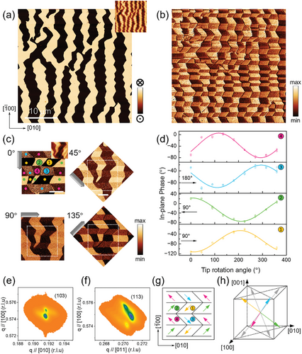
Angle-resolved (AR) PFM was used to reconstruct the directions of the IP polarization variants by changing the azimuthal angle between the cantilever and the sample. This IP PFM technique can sensitively detect the polarization component perpendicular to the cantilever as it relies on the torsional vibration of the cantilever.[40] Therefore, the directions of the IP polarization variants have been resolved by high-resolution PFM images acquired at the quasi-identical region by changing the cantilever-sample orientation from 0° to 360° with an interval of 45°. All the AR-PFM measurements were performed at an off-resonance frequency (100 kHz which is far away from OOP/IP resonance frequency) to avoid cross-talk from the OOP channel or topography. Representative IP PFM phase images at different cantilever orientation angles with four polarization variants are denoted by four different colors, as shown in Figure 1c. Extracted IP phase signals from each color set rather than single points are averaged and plotted as a function of the cantilever rotation angle (Figure 1d). Trigonometric fitting was carried out to determine the directions of polarization. The IP phase differences of domain ③, ②, and ① in comparison to domain ④ are 180°, 90°, and 90°, respectively, as denoted in Figure 1d.
PMN-30PT has a composition close to the morphotropic phase boundary (MPB) that separates the rhombohedral and tetragonal phases. It is believed that at this MPB region, the existence of intermediate monoclinic phases acts as a structural bridge between rhombohedral and tetragonal phases facilitating polarization rotation, which consequently leads to enhanced piezoelectric properties. To further probe the crystal structure and associated domain configurations, high-resolution X-ray diffraction and trailing-field PFM experiments were performed. The X-ray diffraction θ-2θ scan only exhibits (00l) peaks with high intensity implying a very good single-crystal structure, as shown in Figure S2 (Supporting Information). Furthermore, asymmetric reciprocal space mapping (RSM) experiments were performed ≈103 and 113 reflections (Figure 1e,f). The respective twofold and threefold peak splitting ≈103 and 113 RSM mapping as well as the 003 RSM mapping with no peak splitting (Figure S2, Supporting Information) all confirm a monoclinic A (MA) structure.[41, 42] The lattice parameters are calculated as am = 5.683 Å, bm = 5.684 Å, cm = 4.022 Å based on the θ-2θ scan and RSM mappings. Based on the lattice parameters, the crystal is a rhombohedral structure with a slight monoclinic distortion. For simplicity, MA is still used in the following text. With this information, the directions of the IP polarization variants and the reconstruction of their corresponding 3D configurations are further explored. A sequence of IP and OOP poling experiments have been performed to determine the spatial relationship of all the domain variants, as shown in Figures S2–S4 (Supporting Information).[43-45] Therefore, the directions of IP polarization variants projected to the (001) plane with a checkerboard pattern can be resolved (Figure 1g), and their three-dimensional geometry is also shown (Figure 1h). However, compared to the reported four-rhombohedral-variant (4R) structure after poling, this MA also has four variants (4 M) but with both upward and downward polarizations in the out-of-plane direction instead of only having one aligned direction.[5, 28, 46] Consequently, there are only two types of domain walls, i.e., zigzag 180° domain walls (between ① and ②, ③ and ④) and horizontal 71° domain walls (between ① and ③, ② and ④). There are no 109° domain walls in the pristine checkerboard domain structure in contrast to the reported 4R domain structures.[5, 28, 46] To note, the PMN-30PT is an MPB composition with an MA structure, which closely resembles the rhombohedral structure due to the slight structural deviations; therefore, the non-180° domain wall types are actually 71°-like and 109°-like domain walls.[45, 47] For simplicity, they are still written as 71° and 109° domain walls in the following text.
ACP is an emerging method to induce larger enhancement to the piezoelectric and dielectric properties in comparison to DCP, which has been attributed to a higher density of domain walls.[25, 29] Most studies focusing on AC poling of bulk PMN-PT samples utilize low-frequency AC fields (0.01–100 Hz) with amplitude in the range of 2–18 kV (the coercive field of PMN-PT is ≈2.5 kV cm−1).[5, 24-30, 48, 49] However, how high-frequency AC poling impacts PMN-PT single crystals remains to be fully elucidated. Herein, high-frequency AC voltages were applied through the scanning probe microscopy (SPM) tip, and PFM images revealed induced needle domains after the poling process (Figure 2a). The finite element method has been used to simulate the magnitude of the AC electric field generated beneath the tip. As shown in Figure 2b, a tip bias of Vac = 2 V can create an inhomogeneous field with a steep gradient, which decreases from a maximum of 500 kV cm−1 to almost zero within a short depth of 20 nm. The simulation is consistent with previous reports.[50] Therefore, the induced AC electric field by the tip has sufficient magnitude to successfully AC pole the top thin layer of the PMN-PT.
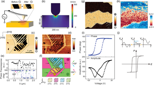
After AC poling at a frequency of 100 kHz by the SPM tip for two passes (for the first pass image see Figure S5, Supporting Information), the large upward zigzag domains are partially switched to the downward direction and form a mixture of upward and downward needle domains with an average width of 110 nm (Figure 2c,d), i.e., from [111] to , and from to (defined within a pseudocubic structure). The switching shows a complete phase reversal of 180° with minimum piezoresponse at the domain walls (Figure 2e). The domain wall density is significantly increased (characteristic domain size reduces from ≈2.5 to ≈110 nm) and needle domain walls are along the diagonal of the x-y plane. It is worth noting that new 109° domain walls form in the needle domain mixtures, which is illustrated in Figure 2f, between the newly switched downward () variant and the pristine upward [111] () domains. A detailed analysis of the switching between different polarization variants was performed by vector PFM measurements, as shown in Figures S6 and S7 (Supporting Information). Domain switching during polarization reversal typically experiences four stages: nucleation of new domains, forward domain growth, sideways motion of domain walls, and back switching.[25, 51] Previous studies have observed a frequency-dependent evolution of domain structures under ACP, i.e., higher frequencies initiate nucleation but not sideways growth.[25] Contrary to this conventional theory, here at 100 kHz of ACP poling, all stages of domain switching appear to occur, indicating a broad spectrum of characteristic switching times. Additionally, this AC poling process also involves both 180° and non-180° domain switching, aligning with a previously proposed multistep stochastic mechanism of switching.[52-54] Nucleation occurs at the 180° domain walls as signified by the white arrows in Figure S5 (Supporting Information), then newly switched domains expand laterally and coalesce at regions close to the previous 180° domain walls (denoted by the black arrows in Figure 2f). Concomitant with the 109° domain switching in the pristine upward domains as discussed above, most of the original 180° domain walls (denoted by black arrows) are replaced by 71° domain walls between domain ④ and domain ② . A new 180° domain wall is also generated between domain ① and domain ② as denoted by the white circle. The coalescence process in the switched domain ② and ④ arises likely due to the energetically more favored downward domains under a strong internal field.
Interestingly, the downward domains are not affected by the AC poling as no needle domains are formed with an AC voltage up to 2.6 V. This is likely due to a synergy of the internal field in the sample favoring one orientation of domain over the other and a decrease of the coercive voltage in the newly formed domain structure. Spatially resolved switching spectroscopy piezoresponse force microscopy (SSPFM) has been used to examine the local electromechanical effect of the sample. Local SSPFM curves were collected from a 50 × 50 grid on a 6 × 6 µm2 area in the off-field bias regime. The amplitude of the AC voltage was chosen to be 0.5 V to avoid the AC poling process. This region has typical upward and downward zigzag domains as shown by the PFM phase image in Figure 2g and the topography in Figure S8 (Supporting Information). The corresponding spatial distribution maps of the positive switching voltage (Vp), negative switching voltage (Vn), and the imprint Vi (Vi = (|Vp|-|Vn|)/2) have been calculated and are shown in Figure S8 (Supporting Information) and Figure 2h. The Vi map reveals a good correlation with the domain structures with the exception of a few poor-quality points toward the end of the scan (upward scanning direction with the slow scanning axis along the y-axis), possibly due to the wear of the tip. The Vi for the upward domains, shown in blue color on the map, has an average value of ≈−0.5 V. The Vi for the downward domains, shown in red color on the map, has a more pronounced imprint, averaging ≈−4.5 V. The larger Vi for the downward domain than the upward domain indicates an energetically more favored state as it requires a higher negative bias for switching to the upward polarization state. This is consistent with the observed immunity of the downward domain against AC poling. The respective topography, Vp, and Vn mapping are shown in Figure S8 (Supporting Information). The 250 groups of SSPFM data taken on both upward and downward domains are averaged, as shown in Figure 2i. The average imprint Vi of the sample is ≈−2.8 V. Such a high degree of imprint is possibly related to defect dipole alignment, i.e., oxygen vacancies in PMN-PT under the poling field, which can pin the domains.[55, 56]
The respective averaged SSPFM data for upward and downward domains are also shown in Figure S9 (Supporting Information). The degree of the imprint is more noticeable in the SSPFM data for individual upward and downward domains. The downward domain requires a large negative bias of ≈−10.7 V for switching to the downward state but needs merely a small positive bias of ≈1 V for back switching, which is consistent with the absence of newly formed needle domains under AC poling in the downward domains, given the small amplitude of the AC bias. The SSPFM data for the upward domain in Figure S9 (Supporting Information) and Vpositive mapping in S8 show positive switching biases within a range between 2 and 5 V. Notably, the AC poling with a peak-to-peak voltage of 2 V can pole the upward domain into downward ones. The discrepancy between the critical amplitude of the bias observed in AC poling and the SSPFM data can be explained below. Some of the upward domains have a switching bias below 2 V for the downward switching, as shown in Figure S8 (Supporting Information). These domains switch first under the AC field initiating the needle domain structure, which can further facilitate the polarization rotation of the whole system due to the ease of switching ability of the needle domains.[56-58] The pristine large zigzag stripe domains in PMN-30PT, as suggested by theory, have a high depolarization field as well as a large elastic energy.[56, 59, 60] AC poling has been shown to break large domains into periodic smaller domains accompanied by a decrease in the coercive field after cycling, and the constantly sweeping high-frequency AC field used here can quickly increase the cycling number.[24, 26, 30] This decrease in domain size can efficiently lower the elastic energy and the depolarization field after reaching an energy equilibrium minimum with the energy cost of the new domain walls. The positive nucleation bias (PNB) and negative nucleation bias (NNB) (inflection points) are also indicated in the SSPFM data in Figure S9 (Supporting Information).[61] The PNB for the upward domain is ≈1.5 V, which means new domains start nucleation but lack sufficient energy for switching. Based on the discussion above, the first-batch needle domains and the AC poling field may lower the overall energy of the system and then result in a lowered switching threshold for the rest of the domains. This explains the low AC switching voltage of the needle domains. Compared to low-frequency poling, high-frequency poling is conducive to the formation of periodic needle domains that do not have sufficient time and energy to expand laterally. The unswitched downward domain under the AC poling field is possibly due to the large internal field (negative) that is equivalent to having an upward shifted AC field with positive amplitude only (Figure 2j), which is consistent with the large Vnegative shown in Figures S8 and S9 (Supporting Information).
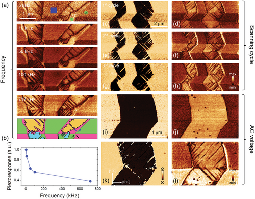
In a further step, the evolution of the domain structures with different AC poling parameters has been investigated. First, the sample was poled at different high AC frequencies from 5 to 717 kHz with an AC bias of 2.3 V, and then PFM images were taken at the same frequency (Figure 3a). The normalized piezoresponse (averaged at the blue box) after the AC polling shows a decreasing trend with increasing AC frequency (Figure 3b). Additionally, obvious variations of the domain structure are observed in Figure 3a. Lower frequencies induce larger switched domains while higher frequencies generate smaller switched domains with a needle structure. These are consistent with the previous report that lower frequency leads to higher saturated piezoresponse as newly switched domains have a longer time to grow and expand, therefore possessing larger domains with fewer domain walls, leading to a longer range of ordering with a more stable domain structure.[25, 26] The domain variants of each domain have been identified with different colors (Figure 3a). It is noteworthy that the newly switched domains, for instance, domain 1 have a slightly higher piezoresponse than the pristine domain 2, which is likely due to tip-injected charges. The schematic in Figure 3a also shows that at the previous 180° now 71° domain walls are weakly charged. PFM results with different cycle numbers in Figure 3c–h show the evolution of needle domain structures under the AC poling field. Increasing the cycle number tends to laterally expand the width of the needle domains given the longer AC poling time. Since the frequency of the ACP used here is quite high and therefore the number of ACP cycles, it is difficult to study the evolution of the piezoelectric performance or domain structure as a function of exact cycle number. Instead, the PFM results were recorded as a function of scanning cycles. Figure 3d,f,h show that no significant piezoresponse enhancement has been observed during the increase of scanning cycles, which can possibly be due to the already saturated piezoresponse after so many cycles (105 cycles/line). Moreover, the critical AC voltage for the AC poling process has been tested to be in the range between 2.0 and 2.3 V below which no switching happens, as shown in Figure 3i–l. The critical AC bias may vary depending on the regions of the sample and the tip conditions. Although the partial switching state of the sample via the AC poling might lead to compromised performance such as high loss and low piezoelectricity, it holds promising applications in the field of optic devices. It is known that the 71° domain walls are light-scattering and 109° domain walls are not, and different proportions of these two domain walls in PMN-PT can lead to different optical properties, such as transmittance, birefringence, and the electric-optic coefficient. Such incomplete switching realized by the high-frequency AC poling can create more than 109° domain walls that have such slanted needle shape, making these optical properties tuneable. This could also potentially be used as engineered optical grating due to such AC-poled domain patterns or novel Q-switches for pulsed lasers.
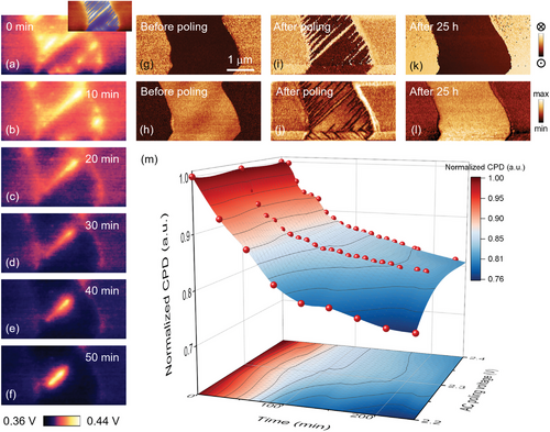
The dynamics of the charge relaxation after the AC poling with varied amplitude, particularly at the domain walls, is of interest, so time-resolved electrostatic properties at the needle domain structures have been investigated. The surface potential of the ferroelectric sample surface is determined by the distribution of space charges, i.e., polarization-bound charges and screening charges.[62] The AC switched needle structure inside the upward domains and the switched region at the edge of the upward domain clearly show a higher contact potential difference (CPD) right after the AC poling, as shown in Figure 4a (also see the superimposed KPFM and PFM image in the inset). PFM images before (Figure 4g,h) and after the AC poling (Figure 4i,j) are also shown. Interestingly, the pristine sample surface before polling shows a polarization-dependent surface potential, which shows a slightly lower (≈10 mV) CPD in the upward domain than that of the downward domain (Figure S10, Supporting Information). It indicates a larger amount of positive screening charges than negative screening charges and is consistent with the observed result. During the AC bias-induced switching, the upward needle domains are over-screened by the tip-injected positive charges. The injected surface charges dissipate gradually and reach an equilibrium, as seen in Figure 4a–f. The charge decays more slowly on the weakly charged needle domain walls and the domain wall between the newly induced 71° domain walls at the edge. The decay of the screening charge is possibly due to the in-plane diffusion of the charges and the recombination of the screening charges of adjacent oppositely polarized domains. The surface adsorptions in the ambient air and the back switching of the AC poled domains can also play a role. Though the back-switching should happen on a longer time scale than the decay of the screening charge demonstrated by the KPFM results. Figure S11 (Supporting Information) shows that after 15 h some of the needle domains can still remain, and after 25 h the AC switched domains back switch entirely (Figure 4k,l). The back switching is caused by the insufficient AC field that cannot form domains penetrating to the bottom electrode and then the domains tend to restore the energetically more favorable downward state. The CPD values of the whole region containing the upward domain and needle domains have been extracted and plotted as a function of time (Figure 4m), which is fitted by an exponential decay function (y = y0 + Ae−x/t where y0 and A being constants and t being the time constant). All three curves show gradual decay over time with no obvious dependence on the AC polling bias. The time constants vary from 51 to 105 min. The time-dependent KPFM images with AC poling biases of 2.2 and 2.3 V are shown in Figures S12 and S13 (Supporting Information).
3 Conclusion
In summary, the crystal structure of a PMN-30PT single crystal has been confirmed as monoclinic MA by XRD reciprocal space mapping, and the unique zigzag (out-of-plane)/checkerboard (in-plane) domain structures originating from the 4 m structure have been carefully investigated by angle-resolved PFM measurements. The PFM and trailing field results demonstrate for the first time the directions of each of the 4 m variants. AC field poling, an emergent method for domain engineering and piezoelectric performance enhancement, has been utilized to study how the high-frequency AC field, rather than the low-frequency field normally adopted, can engineer the domain structures. Needle domain structures are induced by AC poling only inside the upward domains due to a strong internal field, which is also accompanied by 109° domain walls that are nonexistent in the pristine state. AC voltages with different parameters including the frequency, scanning cycles, and amplitude of the bias have been studied to show the influence of the domain engineering. Additionally, the electrostatic conditions of the AC-poled domain structures as a function of time have been monitored by KPFM exhibiting an exponential decay of the tip-injected screening charges at the AC-switched domain structures. Our results show that high-frequency AC poling is a viable approach for domain engineering in PMN-30PT crystals, and this methodology could lead to potential performance enhancement and new topological structures in other ferroelectrics.
4 Experimental Section
Sample Preparation
The 0.7Pb(Mg1/3Nb2/3)−0.3PbTiO3 (PMN-PT) single crystals with (001) orientation were obtained commercially from MTI Corporation, China. The crystals were synthesized by an improved Bridgman method. The size of the crystals is 5 mm × 5 mm × 0.2 mm, two-sided polished with a surface roughness (Ra) less than 10 Å.
X-ray Diffraction Characterization
High-resolution θ−2θ X-ray diffraction studies and reciprocal space mappings were carried out using a PANalytical X'Pert Pro diffractometer with CuKα−1 radiation.
Scanning Probe Microscopy Measurements
All measurements were performed by two commercial AFM systems: an AIST-NT Smart SPM 1000 and an Asylum Research MFP-3D Infinity at room temperature under ambient conditions. The angle-resolved PFM measurements were performed with an AC excitation bias of 1.5 V (peak to peak) with platinum-coated tips (HQ:NSC35/Pt, Mikromasch) at an off-resonance frequency of 100 kHz to avoid any crosstalk from the topography or resonance frequencies. A sinusoidal AC voltage was applied to the tip with an amplitude from 2 to 2.5 V at different frequencies ranging from 5 to 800 kHz. The OOP and IP resonance frequencies of the PFM imaging are ≈740 and 1100 kHz, respectively. Standard PFM imaging at resonance frequencies was performed with an AC bias lower than the critical voltages for the ACP. For switching spectroscopy piezoresponse force microscopy (SSPFM), commercial silicon tips with conductive Ti/Ir coating (ASYELEC.01-R2, Asylum Research) were used. A noncontact mode with a lift height of 10 nm was used for the KPFM measurements to study the electrostatic states of the domain structure after the alternate current poling (ACP).
Finite Element Simulation
To understand the cross-sectional electric field distribution within the tip-surface junction, the objective system was modeled by finite element simulation with a total size of 180 × 80 nm2 for the dielectric matrix and a radius of 30 nm for the sphere tip. The permittivity of the matrix was 3000, which was suitable for lead-based ferroelectric materials at room temperature. The tip was considered to be an inert metal whose permittivity was infinite (i.e., 1 × 10⁸ for this simulation). The tip voltage was set to 2 V, while the bottom edge of the matrix was grounded. These simulation results were reasonable and consistent with the reported values.[63] It was noted that the inhomogeneity of the electrical field generated underneath the tip was related to the tip-surface contact, and the relative permittivity of the material could affect the simulated electrical field.
Acknowledgements
The authors acknowledge support from the Australian Research Council through Discovery Grants and the ARC Centre of Excellence in Future Low Energy Electronics Technologies (FLEET). L. L. acknowledges support from the National Natural Science Foundation of China (No. 12204096), the Natural Science Foundation of Jiangsu Province (BK20220797), the Open Research Fund Program of the State Key Laboratory of Low-Dimensional Quantum Physics (No. KF202203) and the open research fund of Key Laboratory of Quantum Materials and Devices (Southeast University), Ministry of Education, and the Fundamental Research Funds for the Central Universities. L. W. acknowledges support from an Australian Government Research Training Program (RTP) Scholarship. P. S. acknowledges support from the Flinders University start-up grant. Some of the data presented in this work was acquired using instruments at the Mark Wainwright Analytical Centre (MWAC) of UNSW Sydney with the assistance of the personnel, which is in part funded by the Research Infrastructure Programme of UNSW.
Open access publishing facilitated by University of New South Wales, as part of the Wiley - University of New South Wales agreement via the Council of Australian University Librarians.
Conflict of Interest
The authors declare no conflict of interest.
Open Research
Data Availability Statement
The data that support the findings of this study are available from the corresponding author upon reasonable request.


