Charge Transfer Modulation in Vanadium-Doped WS2/Bi2O2Se Heterostructures
Abstract
The field of photovoltaics is revolutionized in recent years by the development of two–dimensional (2D) type-II heterostructures. These heterostructures are made up of two different materials with different electronic properties, which allows for the capture of a broader spectrum of solar energy than traditional photovoltaic devices. In this study, the potential of vanadium (V)-doped WS2 is investigated, hereafter labeled V-WS2, in combination with air-stable Bi2O2Se for use in high-performance photovoltaic devices. Various techniques are used to confirm the charge transfer of these heterostructures, including photoluminescence (PL) and Raman spectroscopy, along with Kelvin probe force microscopy (KPFM). The results show that the PL is quenched by 40%, 95%, and 97% for WS2/Bi2O2Se, 0.4 at.% V-WS2/Bi2O2Se, and 2 at.% V-WS2/Bi2O2Se, respectively, indicating a superior charge transfer in V-WS2/Bi2O2Se compared to pristine WS2/Bi2O2Se. The exciton binding energies for WS2/Bi2O2Se, 0.4 at.% V-WS2/Bi2O2Se and 2 at.% V-WS2/Bi2O2Se heterostructures are estimated to be ≈130, 100, and 80 meV, respectively, which is much lower than that for monolayer WS2. These findings confirm that by incorporating V-doped WS2, charge transfer in WS2/Bi2O2Se heterostructures can be tuned, providing a novel light-harvesting technique for the development of the next generation of photovoltaic devices based on V-doped transition metal dichalcogenides (TMDCs)/Bi2O2Se.
1 Introduction
The interlayer coupling in atomically thin van der Waals heterostructures offers new phenomena such as the opening of a band gap in graphene,[1] band alignment engineering,[2] charge transfer,[3] and enhanced optical absorption.[4] Therefore, in two–dimensional (2D) heterostructures the carrier properties are not dependent on host material only, rather it also depends on the interlayer interactions such as dielectric environment, charge trapping centers, etc.[5] One can tune the thickness of these 2D components involved in 2D heterostructure structures to cover near- to mid-infrared spectral range with strong light–matter interactions.[6] On the contrary, such flexibilities cannot be imagined in conventional 2D heterostructures due to limitations in expensive growth techniques such as molecular beam epitaxy,[7, 8] and metal–organic chemical vapor deposition (MOCVD) etc.[9] To realize the aforementioned 2D heterostructures transition metal dichalcogenides (TMDCs) have already shown great potential exhibiting interesting physical properties.[10, 11] To name a few, WSe2,[12] WS2,[13] MoSe2,[14] and MoS2,[15] with a direct bandgap in visible range and excellent electronic properties are predicted to form type-II heterojunctions.[16] This charge transfer and separation occurring at the heterojunction is very crucial where an exciton created in one material is dissociated into a spatially separated electron–hole (e–h) pair across the interface.[16]
Although 2D heterostructures have shown promising electronic and optoelectronic performances, the intrinsic nature of the materials involved limits the tunability of these heterostructures. For example, pristine MoS2 is n-type[15] whereas WSe2[17] is p-type, which means the heterostructures made from these two materials with a fixed Fermi level (EF) exhibit limited photodiode performance. Therefore, one way to enhance the performance of 2D heterostructures is to control the injection and extraction of electrons/holes, which can achieve n- and p-doping of TMDCs.[18] By modulating the carrier density in TMDCs, their physical properties can be altered on demand. Moreover, the interaction between carriers and excitons in 2D layered materials can lead to PL modulation, resulting in improved optoelectronic device performance. Among the various example of controllable doping to modulate the electronic properties of TMDCs include chemical vapor depostion (CVD),[19, 20] intrinsic defects,[21] charge transfer,[22] chemical intercalation,[23] and electrostatic modulation.[24] However, substitutional doping is advantageous over charge transfer doping using surface adsorbates as later one is prone to thermal desorption.[25, 26]
In our study, we investigate the integration of vanadium (V)-doped WS2,[20] hereafter labeled V-WS2, with Bi2O2Se[27] to control the charge transfer in V-WS2/Bi2O2Se heterostructures. The doping level of V in the V-WS2 is adjusted through a previously established solution-based synthesis method, allowing for modulation of the carrier density in the TMDCs.[20] By manipulating the precursor solutions, optimizing the sulfidation process, and selectively doping the WS2 monolayers with vanadium, we achieve precise control over the density of inherent defects and the charge transfer characteristics within the material. Recently, Bi2O2Se has drawn considerable attention as a new type of novel 2D material. Bulk Bi2O2Se crystals are composed of tetragonal (Bi2O2)n layers separated by Se atomic sheets, coupled by electrostatic forces. This new 2D material shows superior ambient stability, novel mechanical properties, high charge-carrier mobilities,[27, 28] thickness-tunable bandgaps,[29] and novel linear and nonlinear optical properties.[30] These features make 2D Bi2O2Se an attractive material for ultrathin electronic and optoelectronic devices. Indeed, the application of 2D Bi2O2Se in various technologies has been extensively studied, including transistors,[27, 28] photodetectors,[31] and gas sensors.[32] Bi2O2Se has already been explored with other materials such as graphene,[33] and TMDCs[34, 35] to explore its potential in 2D heterostructures.
2 Results and Discussion
2.1 Microscopic Characterization of WS2/Bi2O2Se and V-Doped WS2/Bi2O2Se
Figure 1a–c shows the optical images of WS2/Bi2O2Se and V-WS2/Bi2O2Se heterostructures. Figure 1d–f shows the atmoic force microscopy (AFM) images of WS2/Bi2O2Se and V-WS2/ Bi2O2Se heterostructures with corresponding heights profiles shown as insets. From the AFM images, the thickness of the Bi2O2Se crystals is ≈30–60 nm. The thickness of monolayers of WS2 and V-WS2 is ≈4 nm instead of ≈0.7 nm. This can be attributed to wrinkle, or bubbles introduced during the transfer process.[34]
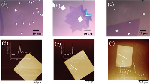
Figure 2a–c displays high-angle annular dark-field (HAADF)-scanning transmission electron microscopy (STEM) images that confirm the presence of substitutional V atoms at W sites in WS2 with minimal dopant aggregation. The use of Z-contrast imaging allows for the clear differentiation of V from the much heavier tungsten, and statistical analysis of HAADF-STEM images at various locations on each flake enables the extraction of its concentration.

2.2 Spectroscopic Characterization of WS2/Bi2O2Se and V-Doped WS2/Bi2O2Se
The Raman spectra of WS2, V-WS2, Bi2O2Se, and their heterostructures have been presented in Figure 3a. Monolayer WS2, belonging to the D3h space group, exhibits characteristic peaks at 355 and 417 cm−1, which are identified as the in-plane E′(Γ) and out-of-plane A1′(Γ) first-order phonon modes, respectively. These peak assignments have been established in the characterization of WS2 and serve as indicators of monolayer thickness.[36-38] The assignment of phonon modes, such as E′(Γ) and A1′(Γ), is based on the symmetry properties of the crystal and the local point symmetries within the WS2 structure. In WS2, E′(Γ) refers to an in-plane phonon mode associated with the E' irreducible representation at the high-symmetry point Γ in the Brillouin zone, while A1′(Γ) represents an out-of-plane phonon mode corresponding to the A1' irreducible representation at Γ. These mode designations provide valuable insights into the phonon behavior and dynamics of WS2 and facilitate a more comprehensive understanding of its structural properties. The apparent blue shift in E′(Γ) and A1′(Γ) with V doping is similar to V-doped MoS2.[39] The emergence of defect-activated longitudinal acoustic mode (LA(M)) with an increase in V concentration hints toward lattice disorder induced by V dopants in V-doped WS2 samples.[40] The increase in V concentration in pristine WS2 results in the suppression of high-intensity 2LA(M) second-order double resonance upon increasing significant changes in the WS2 electronic structure consequently driving the system out of resonance.[20] The Raman spectrum of Bi2O2Se displays a peak at 159 cm−1 that is assigned to the A1g mode of Bi2O2Se.[29] The Raman spectrum of the WS2/Bi2O2Se heterostructures appears to comprise a combination of all Raman modes from the constituent layers.
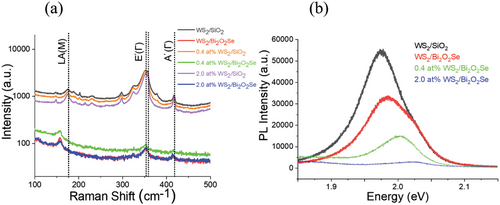
Figure 3a shows that the Raman intensity of both pristine WS2 and V-doped WS2 significantly decreases when they are stacked onto Bi2O2Se to form a heterostructure, which could be attributed to several factors. First, the lattice mismatch between WS2 and Bi2O2Se can create strain in the WS2 layer, affecting its vibrational modes. Second, the annealing process causes charge transfer between the two materials, leading to changes in the electronic properties of the WS2 layer and weakening the bonding strength between the atoms, which in turn reduces the Raman scattering process. Finally, impurities such as oxygen or vanadium can be introduced during annealing, affecting the electronic and vibrational properties of the WS2 layer, and weakening the Raman scattering process. In addition, LA (M) modes shifted to lower frequencies in the case of WS2/Bi2O2Se and doped WS2/ Bi2O2Se heterostructures. This can be due to the fact that the LA (M) mode of WS2 refers to the longitudinal acoustic mode in the WS2 lattice, which involves the collective motion of all atoms in the crystal along the direction of the wave vector. This mode is a phonon mode and can be probed by Raman spectroscopy. When WS2 is stacked onto Bi2O2Se to form a heterostructure, the lattice mismatch between the two materials can create strain in the WS2 layer. Annealing the heterostructure with Bi2O2Se can relieve some of the strain, which can affect the phonon modes in the WS2 layer, including the LA (M) mode. The strain can cause a shift in the LA (M) mode to lower frequencies, as shown in Figure 3a. Furthermore, the annealing process can also improve contact between the materials, causing increased charge transfer between the WS2 and Bi2O2Se layers, leading to changes in the electronic properties of the WS2 layer. This can affect the bonding strength between the atoms in the WS2 layer, which can also contribute to the shift in the LA (M) mode.
Photoluminescence (PL) spectroscopy is performed to further confirm the thickness of the WS2 flake and the charge transfer properties of the heterostructure as shown in Figure 3b. Pristine monolayers of WS2 show an intense PL peak at 1.97 eV, corresponding to the A exciton[30] One can clearly see the quenching in PL intensities once WS2 monolayers were transferred over Bi2O2Se. In Figure 4a–c, we show the PL quenching comparison for pristine WS2, 0.4 at.% V-WS2 and 2.0 at.% V-WS2 heterostructure over SiO2 and Bi2O2Se. The PL is quenched by a factor of 16, 22, and 30 for WS2/Bi2O2Se, 0.4 at.% V-WS2/Bi2O2Se and 2 at.% V-WS2/Bi2O2Se, respectively indicating a superior charge transfer in 2 at.% V-Ws2/Bi2O2Se as compared to WS2/Bi2O2Se. The decrease in PL can be attributed to the strong recombination of charges, as consistently observed in our previous published study[20] where a decrease in PL with doping indicated enhanced charge recombination. Figure 4a–c offers compelling evidence of the significant PL quenching even after transferring WS2 and V-doped WS2 over Bi2O2Se, further reinforcing the role of charge transfer in the heterostructures. This observed decrease in PL can be attributed to the amplified recombination of charges resulting from the doping and charge transfer effects within the heterostructure. In addition to PL quenching, there is a significant shift in PL peak for heterostructures over Bi2O2Se and the peak energy difference is increasing with V doping from 12 to 56 meV.
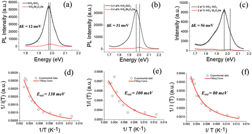
The introduction of V dopants in WS2 leads to a reduction in the bandgap, as observed in our previous study.[20] By comparing PL peak positions in WS2/SiO2 samples at different doping levels, a consistent shift toward lower energy with increased dopants was identified, indicating the modulation of the semiconducting behavior. The shift in the PL peak of WS2 and Bi2O2Se heterostructures could be attributed to the modifications in the electronic band structure of the WS2 layer, which can be caused by various factors, including doping, interface effects, and strain. As V doping increases, the difference in the PL peak shift also increases. The presence of Bi2O2Se modifies the electronic structure of the WS2 layer through charge transfer, and V doping introduces impurity states into the WS2 bandgap, which changes the electronic structure and causes a PL peak shift. Lattice mismatch between the two materials creates strain in the WS2 layer, which also modifies the band structure and contributes to the shift in the PL peak. The interface between the two materials can modify the WS2 band structure and affect the PL peak, and V doping can alter the interface chemistry, resulting in a more significant shift in the PL peak. The combination of these factors is responsible for the observed shift in the PL peak of WS2 and Bi2O2Se heterostructures, and the magnitude of the shift increases with increasing V doping (as shown in Figure 4a–c).
To further investigate interlayer exciton dynamics, we have performed low-temperature PL measurements over WS2/Bi2O2Se, 0.4 at.%V-WS2/Bi2O2Se, and 2.0 at.% V-WS2/Bi2O2Se heterostructures (Figure 4d–f). Therefore, the enhanced charge transfers in case 2.0 at.%WS2/Bi2O2Se heterostructures over WS2/Bi2O2Se, 0.4 at.% V-WS2/Bi2O2Se must result in lower energy exciton binding of the interlayer 2.0 at.% V-WS2/Bi2O2Se heterostructures as compared to WS2/Bi2O2Se and 0.4 at.%V-WS2/Bi2O2Se heterostructures. To estimate the binding energy of WS2/Bi2O2Se, 0.4 at.% V-WS2/Bi2O2Se and 2.0 at.% V-WS2/Bi2O2Se heterostructures, we have utilized the following equation I(T) = I0/ (1 + Ae−EB/kBT) where I0 is the PL intensity at 0 K, EB is the exciton binding energy, and kB is the Boltzmann constant.
The binding energy of interlayer exciton for WS2/Bi2O2Se, 0.4 at.% V-WS2/Bi2O2Se and 2.0 at.% V-WS2/Bi2O2Se heterostructures were estimated to be ≈130, 100, and 80 meV, respectively which is much lower than that for monolayer WS2 (229 meV). These values indicated that 2.0 at.% V-WS2/Bi2O2Se heterostructure shows much efficient charge transfer as compared to 0.4 at.% V-WS2/Bi2O2Se and WS2/Bi2O2Se. The lower exciton binding energy for 2.0 at.% V-WS2/Bi2O2Se heterostructure indicates that the excitons in the heterostructure can dissociate into free carriers easier than pristine monolayer WS2. This is an advantage for 2.0 at.% V-WS2/Bi2O2Se heterostructures as efficient photodetectors. Thus, this result confirms that charge transfer in WS2/Bi2O2Se heterostructures can be tuned via V-doping in WS2.
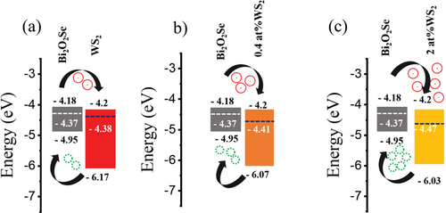
To further gain insights into the charge transfer, we employed KPFM to characterize WS2/Bi2O2Se, 0.4 at.% V-WS2/Bi2O2Se and 2.0 at.% V-WS2/Bi2O2Se heterostructures. The surface potential maps of these heterostructures are shown in Figure 5. The contact potential difference (CPD) between the AFM tip and Bi2O2Se or Pristine and V-doped WS2 can be expressed as CPDBi2O2Se = φtip – φBi2O2Se and CPDWS2 = φtip- φWS2 where φtip, φWS2, and φ Bi2O2Se are the work functions of the tip, WS2, and Bi2O2Se, respectively. The CPD difference of WS2, 0.4 at.% V-WS2, 2.0 at.% V-WS2 and Bi2O2Se corresponds to fermi level differences of WS2, 0.4 at.% V-WS2, 2.0 at.%WS2 and Bi2O2Se with difference being the values ΔEF ≈13, 40, and 100 meV, respectively estimated via line profile of the surface potential as shown in Figure 5a–c.

Figure 5 indicates that the work function of Bi2O2Se is lower than that of WS2, both for 0.4 at.% V-WS2 and 2.0 at.% V-WS2. Therefore, heterostructures of WS2/ Bi2O2Se, 0.4 at.% V-WS2/ Bi2O2Se, and 2.0 at.% V-WS2/ Bi2O2Se form a type-II heterojunction, which can serve as a p–n junction. The built-in potential of these heterostructures allows for the separation of electrons and holes in different regions, leading to efficient charge transfer, as supported by PL quenching.
2.3 Proposed Mechanisms for Charge Transfer Involved in WS2/Bi2O2Se and V-doped WS2/Bi2O2Se
3 Conclusion
In summary, this study presents the experimental demonstration of charge transfer in V-doped WS2/Bi2O2Se heterostructures for the first time. The charge transfer is probed using a variety of techniques, including PL mapping, low-temperature PL, and KPFM measurements. The results show that the PL is quenched by 40%, 95%, and 97% for WS2/Bi2O2Se, 0.4 at.% V-WS2/Bi2O2Se, and 2 at.% V-WS2/Bi2O2Se, respectively, indicating a superior charge transfer in 2 at.% V-WS2/Bi2O2Se compared to WS2/Bi2O2Se. The exciton binding energies for WS2/Bi2O2Se, 0.4 at.% V-WS2/Bi2O2Se, and 2 at.% V-WS2/Bi2O2Se heterostructures were estimated to be ≈130, 100, and 80 meV, respectively, which are significantly lower than that of monolayer WS2. The combination of V-doped WS2 and Bi2O2Se presents an exciting opportunity for the development of advanced photovoltaic devices, photodetectors, and photocatalysts. These heterostructures hold enormous potential for various applications, including environmental monitoring, biomedical imaging, and catalysis. Moreover, their ultrathin p–n junctions make them particularly suitable for use in lightweight and flexible photovoltaic devices such as wearable electronics and electronic textiles.
4 Experimental Section
Synthesis of Pristine and V-Doped WS2 Monolayers
The previously reported CVD synthesis method was used to synthesize both pristine and V-doped WS2 monolayers. Specifically, ammonium metatungstate (0.05 g) and sodium cholate (0.2 g) powders were dissolved in water (10 mL) to prepare the tungsten precursor solution. For the vanadium precursor solution, vanadyl sulfate (0.05 g) powder was dissolved in deionized water (10 mL) to form a 1 × 10⁻² mol L−1 vanadium precursor, and the concentrations of the W and V solutions were controlled to form solution-based cation precursors. Subsequently, the precursor solution was drop-casted onto a SiO2/Si substrate and spin-coated for 1 min at 3000 rpm. The film sulfidation process was carried out at atmospheric pressure in a quartz reaction tube (1-inch inner diameter) with sulfur (400 mg) powder heated upstream at a low temperature of 220 °C using a heating tape. The cation precursor spin-coated on the SiO2/Si substrates was placed in the high-temperature (825 °C) zone, and ultrahigh purity argon was employed as the carrier gas. After a 15-min synthesis, the furnace was allowed to cool to room temperature naturally.
CVD Growth of Monolayer Bi2O2Se
The CVD synthesis of Bi2O2Se was performed in CVD (OTF- 1200X, MTI corporation) under 500 mbarr pressure conditions in a 30-mm diameter quartz tube. Powders of Se (Alfa Aesar, 5 N, 2.0 g) and Bi2O3 (Alfa Aesar, 5 N, 2.0 g) were located in the upstream and downstream heating zones, respectively. Se and Bi2O3 powders were spaced to maintain the required temperature of 240 °C for the Se source and 680 °C for the Bi2O3 powder. Argon (typically 200 sccm) was employed as the carrier gas to transport the precursors onto freshly cleaved fluorphlogopite substrate surface for film deposition. The pressure was kept constant at 500 mbarr during CVD growth.
Fabrication of WS2/Bi2O2Se Heterostructures
The WS2 and V-doped WS2/Bi2O2Se heterostructures were created using two-step process. The first step is to transfer CVD-grown Bi2O2Se over F-mica to SiO2/Si substrates. For this transfer, polystyrene (PS) solution was spin-coated over f-mica substrates containing Bi2O2Se at 3000 rpm for 60 s followed by baking at 85 °C for 15 min. Thereafter, a drop of deionizedwater was used to peel off the PS-coated Bi2O2Se-film from f-mica. Consequently, PS- Bi2O2Se film floating over water was transferred carefully over precleaned SiO2/Si substrates. Next, the Si/SiO2 substrates with PS- Bi2O2Se film was then heated at 150 °C for 30 min to improve the adhesion between the PS- Bi2O2Se film and the underlying substrate. Finally, the PS layer was dissolved by keeping the device in toluene for 2 h followed by acetone treatment for 1 h to remove the organic residuals leaving behind Bi2O2Se over Si/SiO2 substrates. In the second step, a polymethyl methacrylate-based transfer method was employed to transfer monolayers of WS2 and V-doped WS2 over Bi2O2Se containing SiO2/Si substrates. The transferred heterostructures were annealed in low-pressure system under Argon gas at 200 °C for 12 h.
Materials Characterization
Bi2O2Se, monolayer WS2 and WS2/Bi2O2Se were characterized using optical microscopy, atomic force microscopy, transmission electron microscopy, Raman microscopy, PLmicroscopy, and KPFM microscopy. A Renishaw InVia microscope with a Coherent Innova 70C argon-krypton laser at the excitation of 488 nm and a LabRAM HR evolution (Horiba) equipped with a 532 nm laser were used for acquiring the Raman and low-temperature PL spectra using a backscattering configuration and an 1800-line/mm grating. For PL and KPFM measurements, a HORIBA LabRAM Evolution RAMAN Microscope-Smart SPM atomic force microscope with 532 nm laser was utilized. Low-temperature PL measurements were performed on a home-built optical spectroscopy with a 50 × objective using a 532 nm continuous wave laser. The sample was mounted onto a cryostat and cooled down to 77 K by liquid nitrogen. For KPFM measurements, Si tips with Cr (20 nm)/Au (30 nm) coating were utilized and a tip apex radius of <35 nm purchased from NanoAndMore, USA (product: HQ:NSC14/Cr-Au). The tips were excited to oscillate near their resonance frequency of 160 kHz. STEM of the samples was performed in an FEI Talos F200X microscope operating at 200 kV. Aberration corrected STEM imaging using an FEI Titan G2 60–300 microscope, operated at 80 kV with double spherical aberration correction, offering the sub-angstrom imaging resolution. An HAADF detector with a collection angle of 42–244 mrad, camera length of 115 mm, beam current of 45 pA, and beam convergence of 30 mrad were used for STEM image acquisition. For the HAADF-STEM images, a Gaussian blur filter (r = 2.00) was applied (by the ImageJ program) to eliminate noise and enhance the visibility of structural details, while the line profiles of ADF intensity were captured by analyzing raw STEM images.
Acknowledgements
B.C. and F.Y. thank the financial support by the U.S. National Science Foundation (Award #2122044) for this project. This research was partially sponsored by the Army Research Office and was accomplished under Grant W911NF2210109. The views and conclusions contained in this document are of the authors and should not be interpreted as representing the official policies, either expressed or implied, of the Army Research Office or the U.S. Government. The U.S. Government is authorized to reproduce and distribute reprints for Government purposes notwithstanding any copyright notation herein. E.D., M.L., D.Z., Z.Y., and M.T. thank Penn State University for funding.
Conflict of Interest
The authors declare no conflict of interest.
Open Research
Data Availability Statement
The data that support the findings of this study are available from the corresponding author upon reasonable request.


