Thermoelectric Performance Enhancement of Film by Pulse Electric Field and Multi-Nanocomposite Strategy
Abstract
Thermoelectric (TE) film has wide potential application in low-grade waste heat recovery and TE generation due to its quick response and multifunctional integration. Multi-nanocomposite is a promising method to solve the difficulty of maintaining temperature difference and achieving a high figure of merit ZT. However, the depletion layer induced by the multi-nanocomposite typically degrades performance. This study presents a simple and convenient method to solve this problem by pulse electric field (PEF). Prototypical TE Bi2Te3 is selected as the objective film. The strong current density effect of PEF removes the depletion layer among carbon nanotubes (CNT) and Bi2Te3 grains. Thus, the CNT nanocomposite with PEF treatment breaks the trade-off between electrical conductivity and Seebeck coefficient, achieving a power factor of 4400 µW m−1 K−2 which stabilizes after annealing effect to 2920 µW m−1 K−2, a record for Bi2Te3 films. Simultaneously, the self-assembled porosity decreases thermal conductivity via phonon scattering while still maintaining a high electrical conductivity of 3130 S cm−1. Thus, the porosity helps maintain the temperature difference and thereby enables a sharp increase in output power. These results indicate that the combination of PEF and multi-nanocomposite is a new method to enhance TE performance, which would have a potential application in the commercial field.
1 Introduction
Thermoelectric (TE) films are ideal materials to recover low-grade waste heat due to their quick response, multifunctional integration, easier application, and so on. They can be expected to recover microenergy in wearable devices and sensors in IoT society thereby eliminating the need to replace batteries.[1-3] Regarding microharvesting, such as in the milliwatts scale, thermoelectricity presents a higher conversion efficiency and larger potential applications compared to traditional power generation.[2, 4] Commercial application of the TE film requires high conversion efficiency in the low temperature (<423 K) range.[4] Nowadays, some TE films can present high conversation efficiency at room temperature, such as superlattice Bi2Te3/Sb2Te3, metastable Fe2V0.8W0.2Al, and composite Ag2Se/Ag/CuAgSe films.[5-7] However, most of these high-performance films still have the problems of relatively high cost, narrow applicable temperature, etc. While inexpensive thin films like oxides,[8-10] silicides,[11, 12] borides,[13] Heusler alloys,[14, 15] skutterudites,[16, 17] etc., in general, have tended to show lower conversion efficiencies. Enhancement of conversion efficiency is limited mainly by two factors. First, it is difficult to maintain temperature differences in the film. One simple method to solve this is to composite porous layers. The porous interface can scatter the phonon and thereby decrease the thermal conductivity. Second, it is difficult to achieve a high figure of merit ZT just by traditional methods. The ZT value consists of electrical conductivity σ, Seebeck coefficient α and thermal conductivity κ, defined as ZT = α2σ/κ. There are trade-offs among these three TE parameters related to electron and phonon transport.[18, 19] Thus, this makes the TE materials including films have a limitation for the ZT value and conversion efficiency.
To break the trade-off and enhance the TE properties, forming nanocomposites with particular functional materials has been shown to be an effective and simplest method.[20, 21] For example, nanocompositing with a partial metallic network,[22, 23] or coating with a high conductive layer such as done for Cu-Bi0.5Sb1.5Te3/PEDOT:PSS film[24] to optimize interfacial carrier transport, are promising routes, to increase the electrical conductivity and Seebeck coefficient simultaneously. In addition, compositing carbon allotropes such as carbon nanotubes (CNT) is another way to enhance electrical conductivity because of the material orientation effect.[25] And the Seebeck coefficient can increase due to the filtering of low-energy carriers at the interface of the carbon allotrope.[26] However, the thermal conductivity in most cases increases with the increase of CNT content, especially in organic materials, such as PANI and PEDOT: PSS.[27, 28] Controlled porosity has been demonstrated in some cases to enhance high-performance TE materials,[29] and in the case of TE films, porous interfaces can scatter the mid or long-wavelength phonons and thereby decrease the thermal conductivity.[30-32] Multi-nanocomposites including both porosity and CNT were shown to have the possibility to decrease the thermal conductivity caused by the CNT without decreasing electrical conductivity.[33] Moreover, nanoporous structures with isolated holes can be an effective way to maintain the temperature difference in the TE devices due to the reduced thermal conductivity and heat convection. Thereby, it can be seen that multi-nanocomposite of CNT and porosity are effective methods to increase the ZT value and conversion efficiency, and we focus on these methods in the present work.
In the temperature region near room temperature, Bi2Te3 has often been selected as the objective for TE films because it is traditionally one of the highest performance low-temperature TE materials.[34-37] Therefore, there has been much work carried out on Bi2Te3 films.[38-45] In regards to utilizing the enhancement methods of CNT compositing and porosity, which we have particularly focused on in this work, the thermal conductivity of Bi0.4Te3Sb1.6 films decreases to 0.25 W m−1 K−1 by compositing porosity, resulting in the increase of ZT.[46] The TE properties of Bi2Te3 films can also be enhanced by compositing carbon allotropes.[47, 48] However, carriers tend to be scattered at the interfaces, to lead a lower electrical conductivity despite the increase of Seebeck coefficient and the decrease of lattice thermal conductivity caused by the carbon interface. The functions of nanocomposites are always limited by the phase interface and depletion layer between the carbons and Bi2Te3 material. Thus, there is an urgent need to develop a simple method for improving Bi2Te3 performance by inhibiting the depletion layer in the multi-nanocomposite case.
This study presents a simple and convenient method to fabricate TE films with high power factor and ZT value by combining multi-nanocomposite and pulse electric field (PEF). Bi2Te3 films are deposited by a simple direct current (DC) magnetron sputtering at an ambient temperature. The multi-nanocomposite components are porosity and CNT to decrease thermal conductivity and increase electrical conductivity, respectively. The PEF method is selected as a way to remove the depletion layer of the CNT composite and to eliminate the micro defects. The results show that the power factor is enhanced to 4400 µW m−1 K−2 at 313 K by combining multi-nanocomposite and PEF. Although an annealing effect due to higher measured temperature exists, the power factor stabilizes at 2920 µW m−1 K−2. The self-assembled porosity maintains the temperature difference on the material and thereby sharply increases the output power. From this enhancement mechanism, we can propose the technical model of high efficiency and low-cost TE film.
2 Experimental Section
There were two types of substrate utilized to form the films with and without nanocomposite, which thereby can be categorized as as-deposited film and nanocomposite films, respectively. As-deposited films were prepared by depositing films on sapphire, as shown in Table S1, Supporting Information. Nanocomposite films were prepared by depositing films on the nanocomposite substrate of anodic aluminum oxide (AAO) and CNT, as shown in Figure S1, Supporting Information. The AAO substrate was formed by etching Al for about 60 min on sapphire (Topmembranes Technology Co., Ltd., Shenzhen, China). The pore diameter was about 150–200 nm and the pore distance was about 200–300 nm. The multi-walled CNT was distributed using a spin coating of 12.5 mg L−1 suspension, and it was relatively uniform on the AAO substrate.
The Bi2Te3 films were deposited using DC magnetron sputtering to make the films have a polycrystalline structure. The hot-pressed target consists of bismuth and telluride with atomic ratios of 41% and 59%, respectively (CNM Materials Technology Co., Ltd., Beijing, China). The substrate temperature was ambient. The base pressure was lower than 3 × 10⁻³ Pa. The working pressure was set at 0.8 Pa with the argon gas flow of 80 SCCM. The DC sputtering power was 240 W with a deposition time of 10 min. The film thickness of nanocomposite film was higher than that of the as-deposited film due to the volume occupied by porosity and CNT.
The PEF was selected to post-treat the as-deposited films and nanocomposite films for 1 h, as shown in Figure S2, Supporting Information (IT6512D, ITECH Electronic Co., Ltd., U.S.). The direction of pulse current passed through the film along the substrate. The pulse cycle was 1 s and the pulse current was 0.2 A. Film temperature as a function of treated time was recorded by data acquisition (Keysight 34972A, Agilent, U.S.). Accordingly, four Bi2Te3 films were obtained for the as-deposited and nanocomposite films with and without PEF treatment, as shown in Table S1, Supporting Information, named as “as-deposited”, “PEF as-deposited”, “nanocomposite”, and “PEF nanocomposite”.
Measurements of TE properties and microstructure of the Bi2Te3 films were the same as the previous study to analyze the relationship between the structure of multi-nanocomposite and TE parameters.[49] The film thickness of Bi2Te3 film was measured by profilometer (Dektak150, Veeco, U.S.) and was found to be 600 and 1030 nm. As mentioned above, due to the volume of porosity and CNT, the film thickness with multi-nanocomposite increased to some extent. Surface morphology of nanocomposite substrate was observed by an optical microscope to ensure the macro uniformity of composite distribution (OM, DSX5000, Olympus, U.S.). Crystal structure and phase were measured by X-ray diffraction (XRD, DMAX 2400, Rigaku, Japan) with a grazing incidence of 3° in 2θ mode. Small-angle X-ray diffraction (SAXD, SmartLab 9 kW, Rigaku, Japan) patterns were used to confirm the existence of porosity with the current of 200 A and the voltage of 45 V. The surface morphology and roughness were measured by atomic force microscopy (AFM, Nanosurf, Flex-Axiom C3000, Switzerland). The cross-section morphology was measured by scanning electron microscopy (SEM, SUPRA 35, Carl Zeiss Inc., Germany) with energy dispersive spectrometer (EDS) component. The microstructure among the film, porosity, and CNT were observed by transmission electron microscope (TEM, Tecnai G2 F20, FEI, USA). To preserve the composite structure, the TEM samples were fabricated by a focused ion beam (FIB, Crossbeam 550, Carl Zeiss Inc., Germany). Carrier concentration and mobility of the Bi2Te3 films were measured by Hall system (Ecopia HMS-5000, Korea) with a magnetic field of 5500 gauss.
Electrical conductivity and Seebeck coefficient were measured by the integrated system (ZEM-3, Ulvac-riko, Japan). The Seebeck coefficient of each temperature was calculated by the slope of voltage difference versus temperature difference. The temperature differences between hot side and cold side were 20, 30, and 40 K. The resistivity of each temperature was measured for four times with and without the temperature differences. The error bar of resistivity was estimated from the four resistivities above, while that of Seebeck coefficient was approximately 5% from the two-thermocouple measurements.[50] In addition, the measurement accuracy of Seebeck coefficient was 7% according to the commercial apparatus maker. The picosecond time-domain thermoreflectance (TD-TR) technique using a customized focused thermal analysis system based on PicoTR (PicoTherm) was utilized to measure the thermal conductivity of the samples in the cross-plane direction.[51-53] For the measurements, a 100 nm layer of Pt was sputtered on the surfaces of the thin films. The output power with a hot side was measured by a quick sweep mode of SourceMeter (Keithley, 2450, USA). The heat transportation from hot side was observed by an infrared camera (Fluke, Tix580, USA) on a heating stage of 353 K. Measured results of thermal conductivity are listed in Table 1 with error values. The dominant factor to the error was the standard deviation of parameter fitting to observed temperature history curve of picosecond thermoreflectance measurement. Since signal-to-noise ratio of temperature history curves of as-deposited samples were better than nanocomposite samples, errors in thermal conductivity of as-deposited samples were smaller than those of nanocomposite samples.
| Bi-Te films | As-deposited | PEF as-deposited | Nanocomposite | PEF nanocomposite |
|---|---|---|---|---|
| Thermal conductivity [W m−1 K−1] | 1.91±0.04 | 1.41±0.03 | 2.17±0.32 | 1.69±0.28 |
| Electrical conductivity [S cm−1] | 365 | 1060 | 1340 | 3130 |
3 Results and Analysis
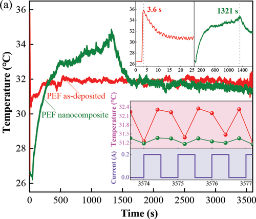
Joule heat was produced by pulse current passing through the film and thereby leading to the temperature change of the PEF films, as shown in Figure 1a. Although the pulse current applied to the film is only 0.2 A, the current density is as high as 333.3 A cm−2. The temperature of the Bi2Te3 films changes near 30 °C upon applying the high-energy pulse current, as shown in the bottom inset of Figure 1a. In addition, the temperature rises to its peak value and then goes down caused by Joule heat and heat radiation, as shown in the top inset of Figure 1a. This is the exothermic effect caused by non-stable atoms transferred to a stable state in the PEF Bi2Te3 film. The time to reach the peak temperature is 1321 s for the PEF nanocomposite film, while it is only 3.6 s for the PEF as-deposited film. After 1321 s, the temperature of PEF nanocomposite film is tending to stabilize with the increase of the treated time. This process is similar to the measurement process of Laser Flash Analyzer (LFA). Both pulsed laser and pulsed current produce heat on the surface of the film, and transfer to the bottom of the film. The film temperature is detected on the substrate side.[54-56] The long time to reach the peak temperature for the PEF nanocomposite film is not only related to the effect of PEF on the depletion layer among nanocomposite interface, but also indicated the lower thermal conductivity of the film. This means that the high current density of the PEF presents a strong effect on the depletion layer.
Treatment of TE film with the PEF is distinguished from other traditional annealing methods, because the PEF just exhibits the strong current density effect and little temperature effect. Furthermore, the pulse current would not lead to a long-term diffusion of Bi and Te atoms.[57] Thus, the Bi2Te3 films with PEF treatment have similar phase, morphology, and element content with those without PEF treatment, as shown in XRD patterns of Figure S3, Supporting Information, AFM images of Figure S4, Supporting Information, and EDS results in Table S2, Supporting Information. Nanocompositing makes the surface roughness of the Bi2Te3 films increase from ≈10 to ≈35 nm. According to Debye–Scherrer formula, the grain sizes of as-deposited film and nanocomposite film are respectively 8.1 and 13.5 nm, while those of the PEF as-deposited film and PEF nanocomposite film are respectively 12.6 and 37.9 nm. Since thin film thickness is much larger than the grain sizes, it is expected that the electrical conductivity and thermal conductivity of this film are not anisotropic but isotropic.
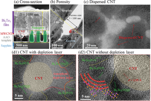
The cross-section morphology, porosity, and interface among CNT and Bi2Te3 grains with and without depletion layer in the nanocomposite film were observed by SEM and TEM, as shown in Figure 2. The film thickness of the PEF nanocomposite film is approximately 1000 nm with a porosity height of approximately 150 nm. The leakage CNT is not only at the bottom of the films, but also encased by deposited Bi2Te3 particles, as shown in Figure 2b. The uniformly distributed CNT interweaves with the Bi2Te3 grains. The SAXD patterns were used to confirm the existence of porosity, as shown in Figure S7, Supporting Information. The strongest diffraction peak appeared near 0.6° with two following weak diffraction peaks. It indicates that the ordered porosity exists in the nanocomposite film and PEF nanocomposite film. Because of the special cone shape of the nanopore, the porous diameter (48 nm) calculated by SAXD is smaller than that observed in Figure 2a. The dispersed CNT is also observed in the TEM result in Figure 2c. Before PEF treatment, there are amorphous areas attaching to the surface of CNT, as shown in Figure 2d1. And the Bi2Te3 (015) and (1010_) grains are not in contact with the CNT. This confirms the existence of the depletion layer before PEF treatment. This depletion layer will lead to a higher carrier concentration and lower carrier mobility. After PEF treatment, the (015) and (1010_) grains are distributed around the CNT, as shown in Figure 2d2. The interplanar spacing of CNT walls is ≈0.335 nm.[26] The Bi2Te3 grains grow along the tangential direction of the CNT without the depletion layer.[47, 48] Thus, the PEF treatment plays a key role to remove the depletion layer of the CNT composite and eliminate the micro defects.
Carrier concentration and mobility as a function of temperature were measured by the Hall measurement system, as shown in Figure 3. PEF treatment leads to the decrease of carrier concentration and increase of carrier mobility, which coincides with the increase of grain size calculated by XRD patterns.[58] The larger grain size contains less grain boundaries, to lead to less Te vacancies caused by the dangling bonds of Te deficiencies at grain boundaries. PEF treatment leads to an increase of grain size, because of two kinds of energy fluctuation. One is the strain energy caused by different orientations in neighbor grains; the other is the energy barrier of atomic diffusion at grain boundaries. High-density pulse current provides Joule heat and current oscillations and induces a pulsed magnetic field,[59] to rearrange the non-stable atoms back to a stable state. In addition, the pulse current penetrating the film is conducive to release the strain energy due to the different conductivity of each orientation in Bi2Te3 crystals. Thus, the PEF provides the driving force of the Bi2Te3 grain growth.
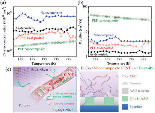
The nanocomposite only slightly increases the carrier mobility despite the high mobility of CNT. This is because the existence of the depletion layer limits the function of CNT on the improvement of TE parameters. However, the increase of defect content caused by nanocomposite increases the carrier concentration. Because there is no depletion layer among Bi2Te3 grains and CNT, regarding the PEF nanocomposite film, CNT would increase the carrier mobility as carrier migration channels.[60] The PEF treatment decreases the carrier concentration while it increases the carrier mobility. In addition, this kind of nanocomposite film may have additional features because the nanocomposite substrate was prepared in the air environment. There were some adsorbed oxygen and some defects on the CNT and AAO template. Due to the substrate being at room temperature, the adsorptive substances cannot volatilize or dislodge during the film growth. The film contains some defects and easily forms a depletion layer among Bi2Te3 grains and CNT. Under this circumstance, the higher carrier concentration and mobility are combined effects of film defects at the interface and the intrinsic transport characteristics. With this nano-structural feature, as shown in Figure 3c, the CNT accelerates the electron migration, while the self-assembled porosity scatters the phonon. Thus, the PEF nanocomposite film can control the electron-phonon transport, to obtain TE films with easier migration of electrons and scattering of phonons.
Listing the films in order of their resistivity from low to high; PEF nanocomposite film, nanocomposite film, PEF as-deposited film, and as-deposited film, as shown in Figure 4a. The electrical conductivities of Bi2Te3 films conform to the polaron model, as shown in Figure S6a, Supporting Information. The linearity of the plots indicates that carrier transport follows small polaron conduction. In this conduction mechanism, the carriers are in a semi-bound state caused by lattice deformation. Impurity ionization, intrinsic excitation, and lattice vibration scattering act comprehensively on electron transport. The resistivity of the as-deposited film from 393 to 433 K slightly increases. This may be caused by carrier scattering on the grain boundary and ionized impurity.[61] Nanocomposite decreases the resistivity compared to the as-deposited film; however, the depletion layer limits the further decrease of film resistivity. Because PEF treatment removes the effect of depletion layer, the resistivity of the PEF nanocomposite film decreases by one order of magnitude to 3.27 µΩ m. Although significant porosity exists in the Bi2Te3 films, pores are located at the bottom of the film and occupy only a relatively small volume because of the height of the nanopores compared with the film thickness. Considering the combined effects of CNT and porosity, the nanopores appear to play a nonsignificant role on the electrical conductivity due to the robust carrier migration channel provided by CNT. Moreover, the electron scattering may be weakened because of the ordered cone-shape nanopore. The electrical conductivity increases while the thermal conductivity decreases at a certain size and distribution of the ordered porosity, which is similar to the behavior observed in Si0.8Ge0.2 films.[26] For the PEF nanocomposite film, the resistivity increases with the increase of measured temperature. This is caused by strong carrier scattering on the interface among Bi2Te3 grains and CNT.[61]

Compared to the films without PEF treatment, as shown in Figure 4b, PEF treatment improves the Seebeck coefficient. The Seebeck coefficient of the PEF nanocomposite film is higher than that of other films due to the lower carrier concentration.[18] Especially, although the carrier concentration of the nanocomposite film is higher than that of the as-deposited film, the Seebeck coefficient of the nanocomposite film is also higher. This may relate to the scattering mechanisms among Bi2Te3 grains and CNT. The carrier mobilities exhibit different temperature dependences at lower temperatures, as shown inserted in Figure S6b, Supporting Information. The temperature exponents were in the range of ≈−1.5–1.5, which indicates the mixed scattering mechanisms of the films.[62, 63] The temperature exponent of the as-deposited film is positive. This demonstrates that the ionized impurity scattering caused by excessive Bi plays a dominant role in carrier transport. The temperature exponents of nanocomposite film and PEF nanocomposite film are −0.11 and −0.28, respectively. The effect of acoustic phonon scattering is more obvious despite the compositing of other phases. This may because of the complex interface caused by multi-nanocomposite, where there exist carrier migration channels of CNT and the carrier activation at the interface. The interfacial energy filtering effect among Bi2Te3 grains and CNT increase the Seebeck coefficient of the film. The mixed scattering mechanisms indicate the unstable state of the films without the PEF treatment. The reason for the unstable state of the Bi2Te3 film is that the films are deposited by magnetron sputtering on room temperature substrate. The low substrate temperature cannot volatilize or dislodge the adsorptive substances on the substrate and the atoms cannot obtain enough energy to have perfect crystallinity growth. Thus, the film contains some defects and easily forms a depletion layer. For the nanocomposite films, the nanocomposite substrate was prepared in the air environment, and therefore, adsorbed oxygen, and some defects on the CNT and AAO template are in an unstable state. Thus, the as-deposited film and nanocomposite films are unstable and might not be appropriate for TE energy conversion applications. Meanwhile, the decrease of the logarithm of the carrier mobility in PEF nanocomposite film versus temperature is approximately linear, indicating dominant acoustic phonon scattering after PEF treatment. This indicates that the lattice coupling at grain boundary was enhanced by a PEF, to promote the acoustic phonon scattering. It may also be that some chemical reactions were triggered by PEF treatment. Chemical reactions caused by PEF might remove the adsorbed substances, defects, and depletion layer in the films. Further work should be conducted to study the chemical reactions caused by a PEF.
The power factor is shown in Figure 4b. The power factor of the as-deposited film is 121 µW m−1 K−2 at 313 K. This value is similar to previous results of polycrystalline Bi2Te3 film.[64, 65] The PEF nanocomposite film exhibits a power factor of 4400 µW m−1 K−2 with an increase of 36 times. This indicates that PEF treatment promotes the functionalities of CNT in the nanocomposite film which leads to the decrease of film resistivity and increase of Seebeck coefficient. The enhancement of power factor is independent of the film phase and orientation, but related to the multi-nanocomposite and PEF treatment. Thus, the PEF nanocomposite film can break the trade-off between electrical conductivity and Seebeck coefficient, and achieved the ultrahigh power factor of 4400 µW m−1 K−2.
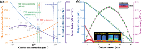
Additionally, improvement of the stability due to the PEF treatment was illustrated by remeasuring the TE parameters of the same PEF as-deposited and nanocomposite films for four times, which are supplied in Figure S5, Supporting Information. The “Initial” is the results of the PEF films measured in March 2019. The “remeasured” are the results of the same PEF films obtained by repeated measurements for four times after two years later in April 2021. The results show that the remeasured resistivities increase by comparing with the initial data, and the remeasured Seebeck coefficients increase. This is because the measured temperature of the initial data is higher than the substrate temperature of the film growth. This higher measured temperature would have an effect like annealing and this leads to the difference between initial data and remeasured data. The PEF treatment can be considered to affect the donor-like defects of non-stable atoms in the Bi2Te3 grains, to weaken the ionized impurity scattering, as shown in Figure 3 and Figure S6b, Supporting Information. After the increase of measured temperature, the grain size increased and the Te vacancies at the grain boundaries decreased, to decrease the carrier concentration. Thus, the resistivities of Bi2Te3 films treated by PEF increase after the first measured cycle. It also indicates that the not fully stable state of the initial PEF films leads to decreasing of the TE properties. However, after the initial change, the remeasured resistivity, Seebeck coefficient, and power factor among these four remeasured data were similar. Although the power factor decreases by comparing to the initial data, it is still the highest value (2920 µW m−1 K−2) achieved in Bi2Te3 films, as shown in Figure 5a. This demonstrates that the PEF treatment improves the stable state, and has the prospect of device stability in practical applications.
Large grain size caused by PEF treatment and the physical characteristics of CNT nanocomposite would typically increase the thermal conductivity of the PEF nanocomposite film. While the self-assembled porosity leads to a decrease of thermal conductivity of the film. The measured out-of-plane thermal conductivity is shown in Table 1. The thermal conductivity of the as-deposited film is 1.91 W m−1 K−1 at 313 K, which is higher than those of Bi2Te3 films.[66] This is due to the higher carrier concentration and the film's morphology of columnar crystals in the as-deposited film. After PEF treatment, the thermal conductivity of PEF as-deposited film decreases to 1.41 W m−1 K−1. This may be related to the phonon scattering caused by the second-phase Bi3Te4, which is consistent with the XRD results in Figure S3, Supporting Information. Nanocompositing CNT and porosity leads to higher thermal conductivity of 2.17 W m−1 K−1 at 313 K caused by higher electronic thermal conductivity. According to the Wiedemann–Franz law (κe = L0σT) with the Lorenz number of (L = 1.5 +e−|α|/116), the lattice thermal conductivity of as-deposited films and nanocomposite films are approximately 1.66 and 1.28 W m−1 K−1, respectively. This demonstrates that the porosity in the film can scatter the phonons, leading to the decrease of lattice thermal conductivity of nanocomposite film.
The thermal conductivity of the PEF nanocomposite film is lower than those of other films in this manuscript (1.69 W m−1 K−1 at 313 K), and the electrical conductivity is the highest (3130 S cm−1 at 313 K). Although the measured directions of thermal conductivity and electrical conductivity are different, the cross-plane value and in-plane value of these conductivities in the Bi-Te films are close to each other because of the small grain size and large film thickness. Furthermore, the lattice thermal conductivity of PEF nanocomposite film is small to negligible. As shown in Figure 3c, the CNT not only accelerates the electron migration, but also increases the phonon transport. Self-assembled porosity was chosen to scatter the phonons, to decrease the thermal conductivity.[30, 31] It can compensate for the increase of thermal conductivity caused by PEF treatment and CNT.[30] In addition, the phonons are scattered by the Bi2Te3 grain boundary and the interface among Bi2Te3 grains and CNT to some extent. The analyzed results suggest that the lattice thermal conductivity decrease by multi-nanocomposite and PEF treatment whereas electrical conductivity increases considerably. The room-temperature ZT values of the as-deposited film, the PEF as-deposited film, the nanocomposite film, and the PEF nanocomposite film are 0.02, 0.06, 0.07, and 0.83. The ZT value of PEF nanocomposite film is higher than those of (00l)-preferred Bi2Te3 film because of its higher power factor caused by CNT nanocomposite and PEF treatment.[67, 68] And this value is similar to that of flexible Bi2Te3 film on CNT scaffold[64] and is comparable to that of bulk Bi2Te3.[69] Hence, the PEF nanocomposite film can control the electron-phonon transport, to obtain the TE film which readily scatters phonon and promoted the migration of electrons.
There is a general competitive relationship between the Seebeck coefficient and electrical conductivity, leading to a limitation of power factor. Thus, Seebeck coefficient, electrical conductivity, and power factor of Bi-Te films as functions of carrier concentrations according to this work and other results are listed in Figure 5a.[58, 64, 68, 70-76] The optimal carrier concentration corresponding to the power factor is in the range of 1019 cm−3–1021 cm−3. In this study, the power factor of PEF nanocomposite film is 4400 µW m−1 K−2 at 313 K, which is higher than those of previously fabricated Bi-Te films. According to previous studies, constructing superlattices, nanocompositing, and doping are effective to enhance the properties of TE film. This power factor in our work is also higher than those of the superlattice Bi2Te3/Sb2Te3 film and the Te-Bi2Te3 film.[5, 66] In addition, the power factor of the PEF nanocomposite film is obviously higher than those of Sb or Se doped Bi-Te films.[77, 78] It can be seen that the improvement of power factor for the PEF nanocomposite film is mainly caused by electrical conductivity enhancement, to exceed the limitation of power factor tuned by carrier concentration. Hence, we propose a cheap and simple method using multi-nanocomposite and PEF to improve the TE performance of Bi2Te3 film by breaking the trade-off among TE parameters. Using Sb or Se doped Bi-Te films as a basis in this method can have the possibility to obtain even better performance.
Improving power factor is conducive to enhance output power, suitable for the waste heat recovery in multifunctional TE generators. Films with porosity have a decrease in the thermal conductivity, which leads to maintaining the temperature difference applied to the films.[32] The output current, voltage, and power of the PEF films at 353 K were measured by SourceMeter, as shown in Figure 5b. The temperature of the heat stage was set as 353 K and the film is vertical to the heat stage. The thermal power is generated by heat dissipation with the ambient temperature of about 298 K. To confirm the ability to maintain temperature difference in the film with porosity, the temperature distributions were observed by an infrared camera. It indicates that the porosity enabled the films to maintain larger temperature differences. This phenomenon is propitious to enhance output power and is expected to solve the problem of maintaining temperature difference in TE film devices. The relationship between the open-circuit voltage V and temperature difference ΔT can be expressed as V = ΔT ×|α|, where |α| of PEF as-deposited film and PEF nanocomposite film were 73.8 and 126.2 µV K−1 at 353 K. Accordingly, the ΔT is about 1.06 and 1.57 K with the length of 2 mm, which are close to the in-plane temperature distribution from the inserted image of Figure 5b.
The internal resistance of the PEF nanocomposite film is about 11.53 Ω while that of the PEF as-deposited film is about 24.12 Ω, in accordance with the resistivity results. The maximum output power of PEF as-deposited film and PEF nanocomposite film were 75.27 and 951.20 pW, respectively. Thus the power density can be determined with the cross-section areas of 0.6 µm × 7 mm and 1.03 µm × 7 mm. The power density of the PEF nanocomposite film is about 0.132 W m−2 at the ΔT of 1.57 K, which is 7.3 times higher than that of the PEF as-deposited film (≈0.018 W m−2 at the ΔT of 1.06 K). The improvement in performance is achieved by enhancement of the power factor of PEF nanocomposite film. The porosity also contributes to maintaining the temperature difference.[32, 79] In these circumstances, the transition length (length with higher temperature gradient) of PEF nanocomposite film is smaller than that of PEF as-deposited film according to the model of the output power density related to temperature distribution.[80] The power density of PEF nanocomposite film is comparable to the Ag2Se/Ag/CuAgSe film (5.42 W m−2) if the temperature difference is enlarged to 45 K.[7] In addition, we obtained a higher power density than 0.1 W m−2 with a smaller temperature compared to those of C60/TiS2[81] and PANi/SWCNT/Te.[82] Therefore, the porosity of the PEF nanocomposite film is of benefit to obtain larger output power by maintaining temperature differences.
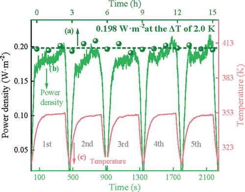
The aging test was performed by measuring the output power density under a temperature gradient for an extended time and under thermal shock for several times. The results are shown in Figure 6. The temperature of the hot side provided by the heat stage is 353 K. The output power was measured per hour for continuing 15 h and the power density was calculated by the cross-section area of 1.03 µm × 2.2 mm. The power density of the remade film device is stable (about 0.198 W m−2) with time. This value is higher than that of the PEF-nanocomposite film in Figure 5b because of a larger ΔT of 2.0 K and a slightly lower power factor of the film. The output power density was also tested under a thermal shock of 5 periods with a drive current of 3.5 µA. The trends of power density and temperature with time are similar. The power density increases with the increase of the hot-side temperature. The peak value of power density is approximately 0.198 W m−2 when the temperature reached 353 K. This result agrees well with the power density in Figure 6a. These results demonstrate that the power generation of the PEF-nanocomposite film is stable when it experiences a constant temperature gradient and thermal shock.
4 Conclusions
This study employed PEF treatment on the multi-nanocomposite to enhance the TE properties of traditional Bi2Te3 films. In the study, the strong current density effect of the PEF was used to remove the depletion layer among CNT and Bi2Te3 grains. This enhanced the function of the CNT on the electrical conductivity and meanwhile dissipated the carrier concentration effect to decrease the Seebeck coefficient due to interface defects. Thus, the CNT nanocomposite with PEF treatment broke the trade-off between electrical conductivity and Seebeck coefficient and achieved the highest power factor of 4400 µW m−1 K−2 for the Bi2Te3 film. The power factor decreased due to an annealing-like effect because of the higher measured temperature and stabilized at 2920 µW m−1 K−2. At the same time, the self-assembled porosity was used to decrease the thermal conductivity to counteract the CNT improvement on phonon transport. The thermal conductivity of the PEF nanocomposite film decreases due to the phonon scattering while still possessing a very high electrical conductivity (3130 S cm−1). Furthermore, the porosity enabled the films to maintain the temperature difference and thereby exhibited a sharp increase in output power. These results presented a simple method to solve the limitation on ZT value by breaking the trade-off of TE parameters and the difficulty of maintaining temperature differences.
Acknowledgements
The authors would like to acknowledge the financial support of the National Natural Science Foundation of China (Grant Nos. 51906033 and 51690161), and the Fundamental Research Funds for the Central Universities (Grant Nos. N180902011, N170908001, and N2025016), and Youth Science and Technology Innovation Talents of Shenyang (Grant No. RC190441). The authors also thank the support from JST Mirai Program Grant Number JPMJMI19A1 and JSPS KAKENHI JP16H06441.
Conflict of Interest
The authors declare no conflict of interest.
Open Research
Data Availability Statement
The data that support the findings of this study are available from the corresponding author upon reasonable request.


