Volume 7, Issue 4 p. 417
Cover Picture

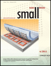
Microcontact Printing: Arrays of Silicon Micro/Nanostructures Formed in Suspended Configurations for Deterministic Assembly Using Flat and Roller-Type Stamps (Small 4/2011)

Yumi Yang

Yumi Yang

Department of Materials Science and Engineering, Gwangju Institute of Science and Technology (GIST), 261 Cheomdan-gwagiro (Oryong-Dong), Buk-Gu, Gwangju 500-712, Korea

Search for more papers by this author
Youngkyu Hwang

Youngkyu Hwang

Department of Materials Science and Engineering, Gwangju Institute of Science and Technology (GIST), 261 Cheomdan-gwagiro (Oryong-Dong), Buk-Gu, Gwangju 500-712, Korea

Search for more papers by this author
Hyun A Cho

Hyun A Cho

Department of Materials Science and Engineering, Gwangju Institute of Science and Technology (GIST), 261 Cheomdan-gwagiro (Oryong-Dong), Buk-Gu, Gwangju 500-712, Korea

Search for more papers by this author
Jung-Hoon Song

Jung-Hoon Song

Department of Materials Science and Engineering, Gwangju Institute of Science and Technology (GIST), 261 Cheomdan-gwagiro (Oryong-Dong), Buk-Gu, Gwangju 500-712, Korea

Search for more papers by this author
Seong-Ju Park

Seong-Ju Park

Department of Materials Science and Engineering, Gwangju Institute of Science and Technology (GIST), 261 Cheomdan-gwagiro (Oryong-Dong), Buk-Gu, Gwangju 500-712, Korea

Search for more papers by this author
John A. Rogers

Corresponding Author

John A. Rogers

Department of Materials Science and Engineering, Frederick Seitz Materials Research Laboratory, Beckman Institute for Advanced Science and Technology, University of Illinois at Urbana-Champaign, 1304 West Green Street, Urbana, Illinois 61801, USA

John A. Rogers, Department of Materials Science and Engineering, Frederick Seitz Materials Research Laboratory, Beckman Institute for Advanced Science and Technology, University of Illinois at Urbana-Champaign, 1304 West Green Street, Urbana, Illinois 61801, USA.

Heung Cho Ko, Department of Materials Science and Engineering, Gwangju Institute of Science and Technology (GIST), 261 Cheomdan-gwagiro (Oryong-Dong), Buk-Gu, Gwangju 500-712, Korea

Search for more papers by this author
Heung Cho Ko

Corresponding Author

Heung Cho Ko

Department of Materials Science and Engineering, Gwangju Institute of Science and Technology (GIST), 261 Cheomdan-gwagiro (Oryong-Dong), Buk-Gu, Gwangju 500-712, Korea

John A. Rogers, Department of Materials Science and Engineering, Frederick Seitz Materials Research Laboratory, Beckman Institute for Advanced Science and Technology, University of Illinois at Urbana-Champaign, 1304 West Green Street, Urbana, Illinois 61801, USA.

Heung Cho Ko, Department of Materials Science and Engineering, Gwangju Institute of Science and Technology (GIST), 261 Cheomdan-gwagiro (Oryong-Dong), Buk-Gu, Gwangju 500-712, Korea

Search for more papers by this author
First published: 01 March 2011
Citations: 2

Abstract

The ability to create and manipulate large arrays of inorganic semiconductor micro/nanostructures for integration on unconventional substrates provides new possibilities in device engineering. Here, simple methods are described for the preparation of structures of single crystalline silicon in suspended and tethered configurations that facilitate their deterministic assembly using transfer-printing techniques. Diverse shapes (e.g., straight or curved edges), thicknesses (between 55 nm and 3 μm), and sizes (areas of 4000 μm2 to 117 mm2) of structures in varied layouts (regular or irregular arrays, with dense or sparse coverages) can be achieved, using either flat or cylindrical roller-type stamps. To demonstrate the technique, printing with 100% yield onto curved, rigid supports of glass and ceramics and onto thin sheets of plastic is shown. The fabrication of a printed array of silicon p+–i–n+ junction photodiodes on plastic is representative of device-printing capabilities.

The full text of this article hosted at iucr.org is unavailable due to technical difficulties.