Film Stress of Amorphous Hydrogenated Carbon on Biaxially Oriented Polyethylene Terephthalate
Corresponding Author
Hendrik Bahre
Institute for Experimental Physics II, Application Oriented Plasma Physics, Ruhr-Universität Bochum, Universitätsstraße 150, 44801 Bochum, Germany
Search for more papers by this authorHenrik Behm
Institute of Plastics Processing, RWTH Aachen University, Pontstraße 49, 52062 Aachen, Germany
Search for more papers by this authorDario Grochla
Institute for Materials, Chair for MEMS Materials, Ruhr-Universität Bochum, Universitätsstraße 150, 44801 Bochum, Germany
Search for more papers by this authorMarc Böke
Institute for Experimental Physics II, Application Oriented Plasma Physics, Ruhr-Universität Bochum, Universitätsstraße 150, 44801 Bochum, Germany
Search for more papers by this authorRainer Dahlmann
Institute of Plastics Processing, RWTH Aachen University, Pontstraße 49, 52062 Aachen, Germany
Search for more papers by this authorChristian Hopmann
Institute of Plastics Processing, RWTH Aachen University, Pontstraße 49, 52062 Aachen, Germany
Search for more papers by this authorAlfred Ludwig
Institute for Materials, Chair for MEMS Materials, Ruhr-Universität Bochum, Universitätsstraße 150, 44801 Bochum, Germany
Search for more papers by this authorJörg Winter
Institute for Experimental Physics II, Application Oriented Plasma Physics, Ruhr-Universität Bochum, Universitätsstraße 150, 44801 Bochum, Germany
Search for more papers by this authorCorresponding Author
Hendrik Bahre
Institute for Experimental Physics II, Application Oriented Plasma Physics, Ruhr-Universität Bochum, Universitätsstraße 150, 44801 Bochum, Germany
Search for more papers by this authorHenrik Behm
Institute of Plastics Processing, RWTH Aachen University, Pontstraße 49, 52062 Aachen, Germany
Search for more papers by this authorDario Grochla
Institute for Materials, Chair for MEMS Materials, Ruhr-Universität Bochum, Universitätsstraße 150, 44801 Bochum, Germany
Search for more papers by this authorMarc Böke
Institute for Experimental Physics II, Application Oriented Plasma Physics, Ruhr-Universität Bochum, Universitätsstraße 150, 44801 Bochum, Germany
Search for more papers by this authorRainer Dahlmann
Institute of Plastics Processing, RWTH Aachen University, Pontstraße 49, 52062 Aachen, Germany
Search for more papers by this authorChristian Hopmann
Institute of Plastics Processing, RWTH Aachen University, Pontstraße 49, 52062 Aachen, Germany
Search for more papers by this authorAlfred Ludwig
Institute for Materials, Chair for MEMS Materials, Ruhr-Universität Bochum, Universitätsstraße 150, 44801 Bochum, Germany
Search for more papers by this authorJörg Winter
Institute for Experimental Physics II, Application Oriented Plasma Physics, Ruhr-Universität Bochum, Universitätsstraße 150, 44801 Bochum, Germany
Search for more papers by this authorAbstract
Amorphous hydrogenated carbon (a-C:H) deposited on steel with plasma enhanced chemical vapor deposition can be used as elongation tolerant oxygen barrier. However, the elongation tolerance of the a-C:H film is lost if deposited on a poly(ethylene terephthalate) (PET) for reasons unknown. To assess this phenomenon, a-C:H was deposited on PET, silicon substrates, and silicon micro-cantilevers, and the stress was determined by measuring the radius of curvature. a-C:H deposited on PET showed lower compressive stress than on silicon. This difference is not due to the formation of a gradient layer or plastic deformation of PET. Instead, the most probable explanation is that energetic ions cause a partial release of biaxial orientation within the PET, thereby reducing the compressive stress.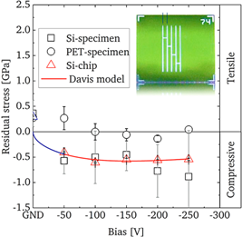
Supporting Information
As a service to our authors and readers, this journal provides supporting information supplied by the authors. Such materials are peer reviewed and may be re-organized for online delivery, but are not copy-edited or typeset. Technical support issues arising from supporting information (other than missing files) should be addressed to the authors.
| Filename | Description |
|---|---|
| ppap201500045-sup-0001-SuppFigs-S1.pdf121.1 KB |
Figure S1: X-Ray photoelectron spectra (C1s core level peak) of a-C:H films deposited on PET and Si substrates with a film thickness of 5 as well as 100 nm. Figure S2: Representative AFM images of PET samples without (a) and with a-C:H films deposited at various bias voltages (b–d). |
Please note: The publisher is not responsible for the content or functionality of any supporting information supplied by the authors. Any queries (other than missing content) should be directed to the corresponding author for the article.
References
- 1 K. Choy, Prog. Mater. Sci. 2003, 48, 57.
- 2 A. Grill, IBM J. Res. Dev. 1999, 43, 147.
- 3 A. Raveh, J. Vac. Sci. Technol. A 1992, 10, 1723.
- 4 J. Damasceno, Surf. Coat. Technol. 2000, 133–134, 247.
- 5 L. Martinu, J. Vac. Sci. Technol. A 1994, 12, 1360.
- 6 F. Richter, K. Bewilogua, H. Kupfer, I. Mühling, B. Rau, B. Rother, D. Schumacher, Thin Solid Films 1992, 212, 245.
- 7 G. G. Stoney, P. Roy. Soc. A Mat. 1909, 82, 172.
- 8 J.-C. Schauer, J. Winter, J. Appl. Phys. 2008, 103, 113302.
- 9 K. Kwong (Apple Inc.) US 2014/0193606 A1, 2014.
- 10 B. Ozkaya, H. Bahre, M. Böke, D. Höwer, S. Reese, J. Winter, G. Grundmeier, Surf. Coat. Technol. 2014, 244, 173.
- 11 Y. Wai Lai, M. Krause, A. Savan, S. Thienhaus, N. Koukourakis, M. R. Hofmann, A. Ludwig, Sci. Technol. Adv. Mater. 2011, 12, 054201.
- 12 C. A. Klein, J. Appl. Phys. 2000, 88, 5487.
- 13 H.-J. Kim, J.-H. Han, R. Kaiser, K. Hwan Oh, J. J. Vlassak, Rev. Sci. Instrum. 2008, 79, 045112.
- 14 N. C. Woo, B. G. Ng, R. Bruce van Dover, Rev. Sci. Instrum. 2007, 78, 072208.
- 15 E. D. Palik, Handbook of Optical Constants of Solids, Academic Press, San Diego, CA 1998.
- 16 A. Ludwig, J. Cao, A. Savan, M. Ehmann, J. Alloys Compd. 2007, 446–447, 516.
- 17 S. Burger, C. Eberl, A. Siegel, A. Ludwig, O. Kraft, Sci. Technol. Adv. Mater. 2011, 12, 054202.
- 18 H. Bahre, K. Bahroun, H. Behm, S. Steves, P. Awakowicz, M. Böke, Ch. Hopmann, J. Winter, J. Phys. D Appl. Phys. 2013, 46, 084012.
- 19 C. Scharwitz, M. Böke, J. Winter, Plasma Processes Polym. 2009, 6, 76.
- 20 C. Srisang, P. Asanithi, K. Siangchaew, S. Limsuwan, A. Pokaipisit, P. Limsuwan, J. Nanomater. 2012, 2012, 1.
- 21 M. A. Tamor, W. C. Vassell, J. Appl. Phys., 1994, 76, 3823.
- 22 C. Casiraghi, A. Ferrari, J. Robertson, Phys. Rev. B 2005, 72, 085401.
- 23
P. Koidl,
C. Wild,
B. Dischler,
J. Wagner,
M. Ramsteiner,
MSF,
1990,
52–53, 41.
10.4028/www.scientific.net/MSF.52-53.41 Google Scholar
- 24 S. Kumar, P. N. Dixit, D. Sarangi, R. Bhattacharyya, J. Appl. Phys. 1999, 85, 3866.
- 25 C. Davis, Thin Solid Films 1993, 226, 30.
- 26 J. Robertson, Pure Appl. Chem. 1994, 66, 1789.
- 27 D. McKenzie, D. Muller, B. Pailthorpe, Phys. Rev. Lett. 1991, 67, 773.
- 28
M. A. Lieberman,
A. J. Lichtenberg,
Principles of Plasma Discharges and Materials Processing,
Wiley-Interscience,
Hoboken, NJ
2005.
10.1002/0471724254 Google Scholar
- 29 A. S. da Silva Sobrinho, J. Vac. Sci. Technol. A 1998, 16, 2021.
- 30 G. M. Whitesides, N. Bowden, S. Brittain, A. G. Evans, J. W. Hutchinson, Nature 1998, 393, 146.
- 31 A. L. Volynskii, S. Bazhenov, O. V. Lebedeva, N. F. Bakeev, J. Mater. Sci. 2000, 35, 547.
- 32 M. M. de Lima, R. G. Lacerda, J. Vilcarromero, F. C. Marques, J. Appl. Phys. 1999, 86, 4936.
- 33 Y. Okada, Y. Tokumaru, J. Appl. Phys. 1984, 56, 314.
- 34Mitsubishi Polyester Film GmbH, Hostaphan RN 50-350, Data Sheet, http://europe-en.m-petfilm.de/wp-blkfxd-0001/uploads/sites/6/Europe_111ENG.pdf (accessed: March, 2015).
- 35 J.-W. Chung, C.-S. Lee, D.-H. Ko, J. Hee Han, K. Yong Eun, K.-R. Lee, Diam. Relat. Mater. 2001, 10, 2069.
- 36 H. Domininghaus, Kunststoffe, Springer, Berlin 2007, pp. 832–833.