Interdigitated back-contact double-heterojunction GaInP/GaAs solar cells
ABSTRACT
Interdigitated back-contact (IBC) silicon solar cells are coming of age, but the potential of IBC configurations for compound semiconductor solar cells is yet to be explored. We outline an approach to generalize the diffusion-driven charge transport (DDCT) method, previously studied for IBC light-emitting diodes, to develop DDCT solar cells, enabling an IBC double-heterojunction structure. In particular, we simulate and compare the electrical performance of a GaInP/GaAs DDCT solar cell with an ideal one-dimensional reference cell to establish how the lateral dimensions of the DDCT structures affect their operation. Also, the suitability of the DDCT solar cells for concentration photovoltaics is explored. The results show that the DDCT solar cells with a finger pitch of approximately 10μm can match and even outperform the ideal reference structure under the AM1.5G solar spectrum, due to reduced Shockley-Read-Hall recombination. At high solar concentrations, the performance of the smallest pitch DDCT structure is essentially identical with the reference structure up to 100 suns. This suggests that combining the benefits offered by the IBC design with compound semiconductors could allow the development of an entire family of more efficient solar cells.
1 INTRODUCTION
The past few decades have seen a rapid development of solar cells with the most advanced state-of-the-art devices being based on interdigitated back-contact (IBC) silicon solar cells,1, 2 efficient single-junction3, 4 and multi-junction5, 6 III-As compound semiconductor cells, and their combinations.7 As compared to silicon, the compound semiconductor cells offer several benefits due to their direct and tunable band gap and composition. Consequently, they presently hold the efficiency record for single-junction solar cells, with the the demonstration of 29.1% efficient GaAs-based thin-film devices,3, 4 but even they still fall relatively far behind their theoretical efficiency limit of approximately 33.5%.8 This has also lead to the recently increased interest in ultrathin III-As solar cells9-11 that can enable higher fill factors and open-circuit voltages. Unlike the further developed IBC silicon cells, however, the efficiency of III-As solar cells is still affected by contact-shading, which can notably reduce the illumination of the cell due to the presence of the metallic front contact-grid as discussed in previous studies.12-14 Despite significant efforts to further increase the efficiency of the III-As cells,13, 15, 16 conventional IBC designs cannot be directly applied to the presently prevailing compound semiconductor solar cells due to the very different carrier diffusion length scales, fabrication methods and surface passivation needs of these materials. Considering the potential benefits, developing IBC designs for III-As solar cells can, nevertheless, bridge the gap between the experimentally demonstrated efficiency for GaAs-based solar cells and its theoretical limit.
The first steps towards IBC technology for compound semiconductor devices were only taken very recently through modelling efforts of emitter-less back-surface alternating contact (EBAC) III-As solar cells17, 18 and diffusion-driven charge transport (DDCT) light-emitting diodes (LEDs).19, 20 On the surface, these devices are similar in the sense that both structures have contacts only on the back and that charge carriers migrate to the active region (AR) through the same surface. In more fundamental terms, however, they have one crucial difference. In the EBAC structure, the current is ‘forced’ to pass through the AR that is still sandwiched between the p-n junction, whereas in the DDCT structure, the AR is parallel to the p-n junction and the current is governed by carrier diffusion even more strongly than in conventional p-n junctions. Therefore, a clear functional difference between these designs is that even if the AR is removed from the DDCT structure, the p-n junction still forms a working device. As such, in terms of current transport, the EBAC solar cell design is very similar to the conventional two-side contacted structures, and it also leaves a significant part of the AR exposed to surface recombination which can substantially reduce the device efficiency, as recently discussed in Myllynen et al19 within the LED context. The DDCT approach does not suffer from such limitation, since both surface and interface recombination can be readily minimized.19 Nevertheless, harnessing the DDCT devices for solving the practical problems in developing IBC technologies for compound semiconductor devices has not been studied.
In this paper, we investigate if the recently proposed DDCT–LED structure19 can enable the development of ultra-thin IBC III-As solar cells. In the studied design, the AR is electrically located parallel to the p-n junctions forming an array of lateral heterojunctions (LHJs) that function as selective contacts for electrons and holes, collecting the photogenerated charge carriers. The DDCT solar cell structure can be fabricated with a straightforward lithography process combined with a p-doping process.21-24 Therefore, realizing DDCT cells should be simpler and easier as compared to the previously studied EBAC designs17, 18 relying on a selective-area growth (SAG) process, which is generally demanding for III-arsenide materials and reported only in a few papers, for example, in other studies.25-27 In addition, originating from the high-power large-area LED context, the DDCT approach provides interesting possibilities for concentration photovoltaics. Also, using DDCT structures as the bottom and/or top cell of a multijunction solar cell can prevent current matching problems, as recently suggested.7, 28, 29 Furthermore, DDCT solar cells can enable applications in more advanced devices such as thermophotonic heat pumps.30, 31 Indeed, our results suggest that the DDCT structures are very well suited for solar cell operation and can even match the performance of an ideal one-dimensional reference device, under both the AM1.5G solar spectrum (1, 000W/m2) and concentrated sunlight.
2 CELL DESIGN AND MODELLING
Figure 1A-C illustrates the complete DDCT solar cell, a single period of the device and the one-dimensional reference device for the simulations, respectively. The lateral dimensions of the DDCT solar cells are designed so that the linewidth (LW) used in the lithography process corresponds to the widths of both the contacts and the separation between them, determining an easily achievable finger pitch. In total, linewidths of 10, 50, 100, 150 and 200 μm are studied, corresponding to structures labelled as DDCT-10, DDCT-50, DDCT-100, DDCT-150 and DDCT-200, respectively. These structures are compared to a reference structure denoted as REF-0, as illustrated in Figure 1C. Structure REF-0 is an ideal vertical solar cell where perfectly transparent contacts cover the top and bottom surfaces. Therefore, REF-0 is essentially a 1D structure where the losses associated with lateral current transport and contact shading are fully eliminated.
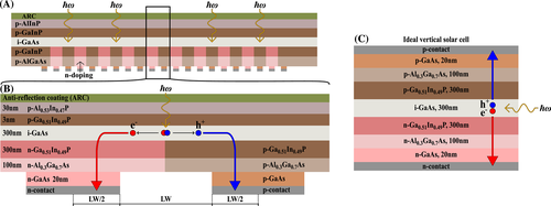
 illustrates incoming photons, and red and blue arrows illustrate the main components of electron and hole currents, respectively [Colour figure can be viewed at wileyonlinelibrary.com]
The DDCT structure in Figures 1A,B uses a 300-nm-thick i-GaAs AR and an array of LHJs located below the AR. The LHJs consist of p- and n-doped 300-nm-thick Ga0.51In0.49P and 100-nm-thick Al0.3Ga0.7As layers that function as selective contacts for the holes and electrons, respectively. Below the LHJs, a 20-nm-thick GaAs contact layer is used in present simulations, but the layer could also be eliminated by contacting the barrier layers directly.9 Above the AR, the structure has a 3-nm-thick p-Ga0.51In0.49P passivation layer and a 30-nm-thick p-Al0.53In0.47P window layer. Additionally, an antireflection coating (ARC) is assumed on the window layer to minimize reflections at the front surface. The DDCT structure can be fabricated with standard processes including device growth with metal-organic vapour phase epitaxy (MOVPE), optical lithography, selective etching and epitaxial lift-off (ELO).32-34 Also, selective area diffusion doping from solid sources21-23 or ion implantation24 needs to be used to form the p-doped regions of the LHJs. The reference structure illustrated in Figure 1C is a planar thin-film solar cell based on a more conventional GaInP/GaAs double-heterojunction (DHJ) structure. Since the main focus of this work is to compare the charge transport in the devices, the DHJ of the REF-0 structure is designed to reproduce the layers where current is transported in the laterally doped DDCT devices.
To simulate the studied solar cells, a combination of charge transport simulations and optical calculations are utilized. Charge transport in the devices is examined by solving the drift-diffusion model equations41-43 connecting the quasi-Fermi levels for electrons and holes and the electrostatic potential. In addition, the well-known ABC model41 is used to calculate the recombination rates for radiative, Shockley-Read-Hall (SRH) and Auger recombination processes. Also, surface and interface recombination rates are estimated as discussed in Sadi et al.44 Table 1 shows the used ABC recombination coefficients and the surface and interface recombination velocities based on well established literature values of state-of-the-art devices. In addition, the electron and hole mobilities for the materials forming the devices are estimated with the empirical mobility model discussed in Sotoodeh et al.45 The optical calculations assume, for simplicity, that all incident photons from the AM1.5G solar spectrum having energies greater than the band-gap energy of GaAs (∼1.42 eV) are uniformly absorbed in the i-GaAs AR. This is justified, since the devices include an ARC, highly reflective back-contacts and ultimately also textured surfaces for redistributing the light through scattering, trapping most of the generated photons within the device.9-11 Furthermore, since this assumption is made for both DDCT solar cells and the reference structure, the relative performance of the devices and therefore the conclusions of this work would remain the same, even if a more detailed optical model would be used. Even more importantly, however, the aim of the present work is to focus on charge transport and to compare different device geometries to one another, providing a detailed view of the electrical behaviour.
For DDCT solar cells, the simulations are performed for one period of the device, extending from the middle of n-contact to the middle of p-contact. Therefore, the simulations include effectively the whole device area assuming a periodically large structure, as justified by device symmetries. Furthermore, the p-doped regions of the LHJs are approximated using square elements in the calculations for simplicity.
3 RESULTS AND DISCUSSION
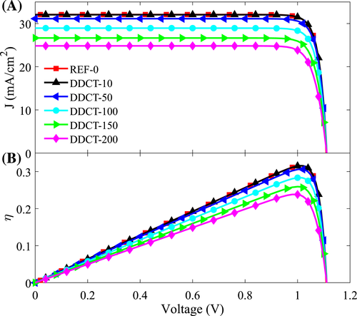
Figure 2A,B presents the output current densities J and the efficiencies η of the simulated solar cells as a function of voltage, respectively, at one sun under the AM1.5G spectrum. The current-voltage J-V characteristics show that the open-circuit voltage Voc is essentially 1.11 V for the REF-0 structure and all the DDCT structures. This value is slightly lower than the theoretical limit of approximately 1.145 V8 originating from the detailed thermodynamic balance between photogeneration and radiative recombination in an ideal device. The identical Voc of the DDCT and REF-0 structures indicates that the lateral transport in the DDCT solar cells does not cause additional voltage losses. Instead, our analysis suggests that most of the (very small) voltage losses revealed in the simulations are attributed to nonradiative recombination and the potential barriers formed due to the band offsets at material interfaces that are similar in both device types. The impact of the lateral dimensions of the DDCT solar cells is, however, clearly reflected in the short-circuit currents Jsc of the devices. While the Jsc ∼32mA/cm2 of the DDCT-10 structure is essentially identical to that of the REF-0 structure, and Jsc generally decreases as the width of the DDCT devices increases. This observation is mostly explained by the low hole mobility and relatively low carrier lifetimes leading to moderate carrier diffusion lengths and poor hole spreading, which degrades the performance of wider devices. A similar trend is observed also for η in Figure 2B. For the DDCT-10 structure, η is similar to that of the REF-0 structure, but it starts to decrease as the LW of the DDCT solar cells increases. Overall, the performance of the DDCT-10 structure is comparable to that of the REF-0 structure, indicating that the DDCT structure does not inherently degrade the solar cell performance, as compared to the ideal one-dimensional reference structure.
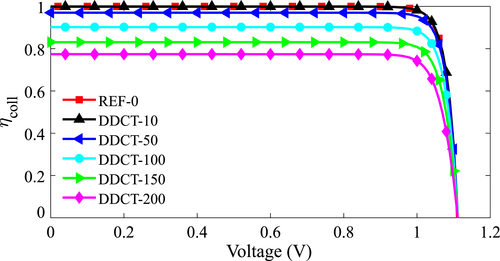
The trend of reduced performance in wider DDCT solar cells can also be explained by analysing the collection efficiency ηcoll of the devices, which is shown in Figure 3 as a function of voltage. ηcoll is defined as the ratio of carriers extracted from the structure to the total number of photogenerated carriers. For the REF-0 and DDCT-10 structures, ηcoll is approximately unity up to 0.9 V. Beyond this voltage, ηcoll starts to decrease as the operation point of the devices starts to shift towards the LED regime. For the wider DDCT structures, ηcoll decreases as the width of the devices increases. This is reflected in the J-V curves in Figure 2A whose shape are identical to that of the ηcoll curves in Figure 3.
In Table 2, we present the figures of merit for the studied solar cells. In addition to the Voc and Jsc already discussed after Figures 2 and 3, Table 2 shows the efficiency ηmpp, current density Jmpp, voltage Vmpp and fill-factor FF of the devices reached at the maximum power point (MPP). The most interesting finding here is that the performance of the DDCT-10 exceeds that of REF-0 at the MPP. This is indicated by ηmpp and Jmpp being slightly higher for the DDCT-10 structure. This unexpected observation is enabled by the reduced SRH recombination rate in the DDCT structures that was first reported in our recent work.19 Essentially, since the AR of the DDCT solar cells is mostly surrounded by p-doped Ga0.51In0.49P layers, the most relevant depletion region is formed inside the AR close to the n-Ga0.51In0.49P/GaAs interface. Also, because most of the SRH recombination occurs at this depletion region, the volume where it takes place is effectively halved, and therefore its rate is reduced. The REF-0 structure does not show a similar effect because the depletion region extends throughout the AR. In contrast to the DDCT-10 structure, performance of the wider DDCT structures is not visibly affected by the minimized SRH recombination due to other losses related to lateral current transport being more pronounced. The FF of the solar cells falls only slightly as the device width increases.
| Structure | Voc(V) |
 |
ηmpp (%) |
 |
Vmpp (V) | FF (%) |
|---|---|---|---|---|---|---|
| REF-0 | 1.11 | 32.1 | 31.5 | 30.9 | 1.02 | 88.6 |
| DDCT-10 | 1.11 | 32.0 | 31.6 | 31.3 | 1.01 | 88.7 |
| DDCT-50 | 1.11 | 31.1 | 30.7 | 30.4 | 1.01 | 88.6 |
| DDCT-100 | 1.11 | 28.9 | 28.4 | 28.1 | 1.01 | 88.2 |
| DDCT-150 | 1.11 | 26.7 | 25.9 | 25.9 | 1.00 | 87.5 |
| DDCT-200 | 1.11 | 24.8 | 23.8 | 24.3 | 0.98 | 86.4 |
In Figure 4, ηmpp of the solar cells is presented for concentrated sunlight from one to 1,000 suns. Up to 100-sun concentration, the performance of REF-0 and DDCT-10 structures is almost identical. At higher concentrations, ηmpp for both devices decreases due to the increased carrier concentration in the AR leading to stronger radiative and nonradiative recombination. This reduces the photogenerated current that is collected at the electrical contacts. The DDCT-50 structure has a slightly increased ηmpp at the 10-sun concentration, but at 100-sun concentration, its performance starts to decrease. In contrast to REF-0, DDCT-10 and DDCT-50 structures, wider DDCT structures (including DDCT-100, DDCT-150 and DDCT-200 structures) do not benefit from increased concentrations due to the large contact separation. In these wider structures, a significant part of the generated charge carriers recombine before they are collected at the electrical contacts.
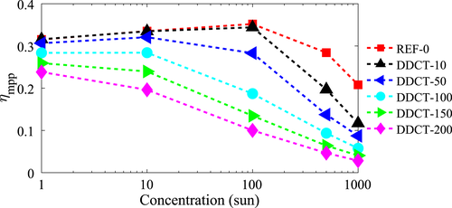
As our results show, the efficiency of the DDCT solar cells strongly depends on the concentration factor and the finger pitch, and the performance of the wider structures DDCT-100, DDCT-150 and DDCT-200 is already strongly limited by the insufficient lateral diffusion of charge carriers. Furthermore, additional simulations have indicated that the performance is also affected by the absorber thickness in some cases. For instance, increasing the absorber thickness to 1,200 nm notably improves the efficiency of the structures with linewidths larger than 100 μm at single-sun illumination. In contrast to wider structures, using a 1,200-nm-thick absorber would marginally reduce the efficiency of the narrower structures DDCT-10 and DDCT-50. For all practical purposes, however, the structures with a finger pitch of the order of 10 μm seem to provide the best compromise between performance and fabrication requirements: the fabrication of devices with a 10-μm finger pitch should already be straightforward with standard UV lithography and such linewidths will provide a very high performance for any absorber thicknesses. To inspect how even smaller linewidths affect the cell performance, we also simulated a DDCT solar cell with a finger pitch of 2 μm that resembles the lower limit of LW that should be possible to fabricate with standard processes. However, reducing the LW below 10 μm does not provide additional benefits for the devices. In this sense, our results indicate that 10-μm LW is indeed optimal for the DDCT solar cells.
The high efficiency predicted by the simulations above suggests that IBC solar cells using DDCT are a promising concept for compound semiconductors. Overall, this study and previous work on EBAC solar cells17, 18 indicate that III-As solar cells can benefit from back-contacted designs and eliminated contact shading. However, these structures are quite different from the earlier experimental III-As solar cell designs46, 47 that have contacts on the back-side without strictly utilizing the IBC design. Instead, in Hong et al,46 p-type via contacts were deposited directly on the AR, while in Cruz-Campa et al,47 n-contacts were fabricated by etching through the AR and contacting a window layer that also functioned as a current-spreading layer. Both approaches resulted in a rather poor conversion efficiency due to several reasons. First, these structures included numerous recombination sites for nonradiative interface and surface recombination. Second, the via contacts used, for example, in Hong et al,46 were nonselective which further increased nonradiative recombination and current leakage. Finally, in the design from Cruz-Campa et al,47 the volume of the AR and thereby the amount of absorbed light were significantly reduced. Overall, these experimentally studied designs would benefit from the eliminated contact shading if the otherwise nonoptimal designs could be improved. From the design point of view, the DDCT solar cells suggested in the current work should be able to overcome all of the aforementioned problems. However, such structures have not been experimentally demonstrated yet. Therefore, developing a fabrication process for the DDCT solar cells is imperative in the future for the realization of IBC III-As solar cells.
4 CONCLUSIONS
In conclusion, this work suggests a successful strategy to harness the benefits of IBC cells, conventionally available only for silicon cells, on the compound semiconductor platform. Our results show that, under the AM1.5G solar spectrum, the performance of laterally doped back-contacted III-As DDCT solar cells can be superior even to an ideal one-dimensional reference structure, which is essentially a GaInP/GaAs DHJ solar cell where all lateral current transport and contact losses are eliminated. Furthermore, the DDCT structure with a 10-μm finger pitch shows similar performance to the reference structure under concentrated sunlight up to 100 suns. As such, the new DDCT solar cell design has several advantages over conventional III-As solar cells, allowing to eliminate contact shading while still enabling nearly ideal current spreading. This indicates that adopting new current-spreading solutions might enable a paradigm shift for the current collection geometry of compound semiconductor solar cells.
ACKNOWLEDGEMENTS
This project has received funding from the Academy of Finland and the European Research Council (ERC) under the European Union's Horizon 2020 Research and Innovation Programme, Grant Agreement No. 638173 and 825142. The authors acknowledge the support from the Academy of Finland Flagship Programme, Photonics Research and Innovation (PREIN).


