Two-dimensional photonic metasurfaces for slow light-controlled photocatalysis
Abstract
Photocatalysis using semiconductor materials like titania (TiO2) is a key method for environmental purification or solar fuel generation. Nanostructures that maximize incident light absorption are highly desired to enhance depollution rate or solar-to-fuel conversion efficiency in limited volumes of catalysts. Here, we report on structural and optical properties of metasurfaces based on a 20 nm thick anatase layer conformally deposited onto a wavelength-scale two-dimensional periodic photonic lattice. We investigate the NO degradation using such metasurfaces, and evaluate the impact of the patterning on photocatalytic activities between 340 and 400 nm. In the 380–385 nm range, the mean photochemical efficiency is increased by a factor up to 5.7 compared to flat references, with an overall three-fold enhancement within the whole spectral range of interest. This approach can be applied to numerous types of systems by varying active materials, leading to substantial improvements in air/water depollution, water splitting or artificial photosynthesis processes.
1 INTRODUCTION
Semiconductor based photocatalysis is generating considerable interest as a mean to tackle current challenges such as depollution and solar energy conversion.[1] Still, the performance of the photocatalytic systems are hindered by a low quantum efficiency due to recombination of the charge carriers and the capacity to harvest only a fraction of the solar spectrum due to the large band gap of the semiconductors involved (3.0 to 3.2 eV for titania [TiO2]). In order to address these issues, intensive work has been carried out, leading to the emergence of a wide range of nanoscale photocatalysts[2-4] such as two dimensional nanomaterials where the bulk electron-hole recombination is minimized.[5] Moreover photocatalyst doping was considered to generate states in the gap in order to narrow the band gap.[6-8] Other strategies involve nano-objects like plasmonic metallic nanoparticles in order to increase incident light absorption and subsequent charge separation.[9, 10] However, these methods have drawbacks and can limit the overall efficiency of the photocatalyst, since narrowing the band gap also decrease the driving force of the reaction[11-13] and the use of plasmonic particles leads to parasitic photon absorption in metal.[14]
Periodic dielectric lattices like photonic crystals are key building blocks which enable a spatial and temporal control of photons at the scale of their wavelength. Such photonic lattices consist of regularly patterned layers, with patterns size of the order of the wavelength. While the involved materials and configurations may be very diverse, most of the demonstrations and practical applications were based on dielectric or transparent semiconducting layers with thicknesses in the wavelength range, patterned as two dimensional lattices or in other words periodic metasurfaces. These structures have been used to generate high quality factor slow light Bloch modes, or, as a more recent example, bound states in the continuum.[15] This has been extensively investigated with a view to develop ultra-compact surface-emitting lasers,[16] single photon sources[17] or non-linear optical devices.[18] Similar platforms have also been developed and combined with absorbing media, in order to collect and convert incident light to realize novel generations of light-trapping assisted photovoltaic solar cells.[19] This approach has stimulated the synthesis of a large diversity of photonic structures combining active absorbing semiconducting media with complex structures, including periodic, multi-periodic,[20] and disordered patterns.[21] Indeed, controlling the complexity and the regularity of the pattern leads to the generation of multiple optical resonances with moderate quality factors, suited to the trapping of incident light with a low coherence like sunlight or light emitted by LEDs.
Subwavelength periodic lattices are then suited to control and convert incident light within a wide wavelength range, as required for photocatalytic applications. Recent results have shown how complex structures such as three dimensional inverted opals[22-25] enable the control of photocatalytic reactions. They are generally realized on the basis of a three dimensional periodic assembly of silica or polymeric sub-micron spheres, subsequently infiltrated by materials that exhibit relevant optical and catalytic properties. This approach was investigated with a view to develop structures such as plasmonic-photonic[23] or photonic crystal[24] heterostructures assisting photocatalysis, or metal loaded TiO2 inverted opals dedicated to photocatalytic reduction of CO2.[25] However, fabricating such complex three dimensional structures is costly and based on very low throughput processes.
In our approach, we propose to generate a two dimensional metasurface including a simple and transparent photonic lattice with wavelength-scale patterns, which can be realized by high throughput processes like nanoimprint. This photonic lattice acts as a light trapping medium; it can be covered by an absorbing layer acting as the photocatalyst with a thickness well below the optical wavelength so as to inhibit photocarrier recombination. The latter assists the chemical reaction using the UV light trapped by the photonic lattice. In this paper, we demonstrate the interest of this approach using a small amount of anatase TiO2 as the photocatalytic medium deposited onto a silicon nitride photonic lattice. We show that using this active metasurface, the photocatalytic oxidation of NO is increased by a factor higher than two for wavelengths shorter than 370 nm. Around 380 nm, the efficiency increase even reaches a factor of 5.7, owing to photon lifetime enhancement by the slow light resonances generated by the periodic photonic lattice. This light trapping assisted by slow light is therefore proposed as an efficient strategy to enhance various kinds of photocatalytic processes that would contribute to air or water depollution, like in the case of NO oxidation, or generate solar fuels with more complex catalysts.
2 RESULTS AND DISCUSSION
2.1 Design and fabrication
The active metasurface includes a SiNx layer, fully transparent in the wavelength range of interest (see Figure S1), with a thickness of 200 nm, periodically patterned as a two-dimensional lattice of air holes, with a wavelength scale lattice parameter and hole radius around 100 nm. Such a photonic lattice couples light from the incident medium (air in the present study) to in-plane Bloch modes. This leads to a diversity of optical resonances, depending on the coupling efficiency and the interaction between coupled Bloch modes. The hole depth can be tuned between 100 and 200 nm, enabling to control the degree of perturbation of the incident optical waves and the vertical symmetry of the photonic lattice. A conformal 20 nm thick TiO2 layer, in strong interaction with the photons trapped by the periodic lattice, is then deposited on top of this lattice to constitute the active layer of the metasurface, as shown in Figure 1A. This thickness corresponds to a trade-off leading to a reasonable incident light absorption and limited recombination of photogenerated carriers.
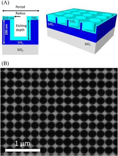
To achieve the fabrication of this complex medium, dedicated technological processes have been developed, leading to a wide nanopatterned area compatible with photocatalysis experiments. SiNx layers are deposited by PECVD and then covered by a negative based photoresist subsequently patterned by two-step interference lithography. Transfer into SiNx is performed by reactive ion etching (RIE), the holes depth being controlled by the etching kinetics. Lastly, the TiO2 layer is deposited by plasma-enhanced atomic layer deposition (PE-ALD). Figure 1B shows the surface of the nanopatterned photonic media before the final TiO2 deposition, which illustrates the fairly high regularity of the holes, with a size dispersion of about 10%. This technological approach, and in particular laser interference lithography, enables the fabrication of centimeter square samples, with a possibility of upscale up to at least 3′ wafers. Such large area samples are required to perform photocatalysis experiments. For the sake of comparison, flat samples are prepared using the same deposition processes, leading to the same thicknesses.
2.2 Structural characterization
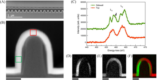
The structural properties and the geometry of the nanopatterned medium were investigated, using dedicated and simplified samples including one-dimensional periodic structures composed of air slits and SiNx:TiO2 ridges. Such a one-dimensional periodic structure is well suited to lamella preparation and can be thoroughly analyzed by scanning transmission electron microscopy (STEM) and electron energy-loss spectroscopy (EELS). Figure 2A shows a cross-section micrograph of such a metasurface with vertical SiNx sidewalls, except close to the top of the layer where the profile is tapered, corresponding to a gradual increase of the air slit width. TiO2 deposition by PE-ALD leads to a very high conformality, with a homogenous layer thickness of 20 nm over the whole surface. The crystallinity of the TiO2 layers was analyzed using STEM-EELS. In this first sample, both amorphous and anatase TiO2 are observed, respectively on the top and bottom surfaces and on the sidewalls (see Figures 2B, 2D–2F), and confirmed by the Ti-L2,3 fine structures shown in Figure 2C, which are a signature of the TiO2 degree of crystalinity[26] and crystal structure.[27-30] The distribution of amorphous and anatase TiO2 was confirmed in multiple areas of the TEM specimen (see Figure S5 and S6). As an additional feature, a SiOx intermediate layer has been observed below the TiO2 layer (see Figure S4), which may play a role in the carrier lifetime of the structure under operation.
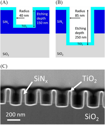
In order to perform photocatalysis experiments, two series of samples (A and B-types) comprising two dimensional arrays of air holes with a 237 nm lattice parameter were fabricated. A-type samples include 40 nm holes radii after TiO2 deposition and etching depths around 150 nm (see Figure 3A), while B-type samples include a stronger corrugation, with 85 nm hole radius after TiO2 deposition, and a 250 nm etching depth (see Figure 3B). Contrary to one dimensional patterns shown in Figure 2, several ultra-thin TEM lamella fabricated out of two dimensional patterns would be necessary to extract lateral sizes of the structures with certainty. Therefore STEM analysis was carried out to assess the TiO2 layer conformality and to verify that the general shape of the patterns is well preserved, as shown in Figure 3. Most importantly, STEM-EELS analysis demonstrates that the whole TiO2 layer is crystalized in the anatase phase (see Figure S7), which is a key condition to achieve efficient photocatalysis. Our synthetic results suggest that the differences in terms of geometry and crystallinity between samples including one and two dimensional patterns are related to the influence of the surface geometry on key parameters of the RIE and ALD processes, like thermal and electrical behavior or surface diffusion. While their investigation is beyond the scope of this study, such properties should be taken into account in evaluating the global efficiency of these complex media.
2.3 Optical properties of metasurfaces
With a view to assess the optical characteristics of these active two dimensional metasurfaces, we first measured their optical transmission spectra in the case of A and B-type samples and flat references, using spectrophotometry at normal incidence. These results are compared with simulations performed using rigorous coupled wave analysis (RCWA, see Experimental Section/Methods), as shown in Figures 4A–4B. In A-type samples (Figure 4A), two main resonances are observed, corresponding to dips in the transmission spectra at 365 and 385 nm. There is a good correspondence between simulation and experiments in terms of general shape, intensity and dip wavelength. There are, however, unavoidable discrepancies that we attribute to uncertainties in terms of dielectric constants of TiO2 and minor inaccuracy of the geometrical parameters measurements. In B-type sample, the main resonances appear between 365 and 385 nm. The correspondence between simulation and experiments is fairly good for 85 nm holes radii after TiO2 deposition, and a 250 nm etching depth, with some differences, notably in terms of amplitude and resonance wavelength. These higher discrepancies can be attributed to the hole size dispersion, which is higher in case of sample B, and may reduce the amplitude and enlarge spectrally the resonances.
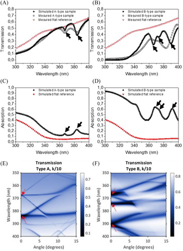
Owing to the correspondence between simulation and measurements, the absorption efficiency of A and B-type samples can be estimated using RCWA simulation, using the same opto-geometrical parameters as for the transmission spectra. Figures 4C and 4D show the absorption spectra for both the active metasurfaces and reference unpatterned samples, simply consisting of a 200 nm SiNx flat layer on SiO2, then covered by a 20 nm thick TiO2 layer. In the short wavelength range, up to 360 nm, the absorption is continuously increased for both samples in the case of the metasurface. While an absolute absorption increase by a factor of two is observed for the A-type sample, it is significantly higher for a B-type sample, with a four-fold enhancement around 330 nm. In this range, considering the high absorption coefficient of TiO2, no clear resonance can be excited, but the enhancement can be explained by two main factors. Firstly, the TiO2 volume in A-type samples is higher than the reference samples by a factor of VA/Vref = 1.75; in the case of a B-type sample, the active medium volume is higher: VB/Vref = 3.25. Secondly, incident light coupling into the metasurface is more efficient than in a flat reference layer, which can be attributed to channeling modes, as demonstrated in absorbing photonic crystals,[31] or simply a better effective index matching. Both effects are enhanced in the case of deeper holes, which is coherent with the higher absorption increase in the case of a B-type sample. Above 360 nm, clear absorption peaks are observed, corresponding to an increase by a factor up to 3.5 in the case of the A-type sample and up to 13 in the case of a B-type sample. Even for off-resonance wavelengths, there is a substantial absorption increase, by a factor exceeding five for B-type samples. Therefore, both in the short and long wavelength ranges, optical characteristics of the photonic metasurfaces are expected to increase in a substantial way the rate of chemical reactions controlled by incident UV light, in particular in the case of the deepest nanopatterns.
Angle-resolved simulated transmission maps are displayed in Figure 4E; this shows the active metasurface photonic band structure. On this graph, an artificially reduced absorption coefficient is considered for TiO2 to highlight the bands without perturbing their spectral position (see Experimental Section/Methods for details). While these metasurfaces exhibit many photonic bands, only a few can be used to efficiently couple incident light from free space and may lead to resonant absorption in TiO2. These bands can be observed close to normal incidence (at 0°) and correspond to the dips on the transmission spectra, and the absorption peaks. The calculated band structures reveal the origin of the peaks observed in Figures 4C–4D. While all correspond to degenerated modes at normal incidence, most of these results from incident light coupling to flat bands, while the one at 390 nm for B-type sample corresponds to photonic bands with higher slopes. Therefore, while this high wavelength resonance results from fast-light modes, we attribute the resonances around 365 and 375 nm for B-type sample, and both resonances for A-type sample to slow light modes around the center of the first Brillouin zone (Γ-point). These are typical modes of a C4-symmetry periodic square lattice of holes, where only photonic modes with a limited quality factor are used since they enable efficient coupling of incident light from free space, especially for B-type sample.[32, 33] In this respect, it should be noted that the slow light resonances exhibit a relatively stable wavelength position with regard to the angle of incidence, for the benefit of the angular acceptance of the metasurface.
2.4 Photocatalytic studies of NO degradation
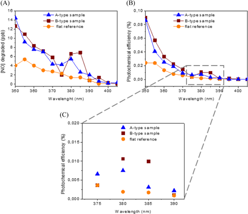
As a case-study, the photocatalytic depollution reaction NO + 1/2O2 + H2O + UV → NO2 + H2O was performed on the A and B-type two dimensional metasurfaces, and on planar references. Figure 5 shows the detected quantity of oxidized NO as a function of the incident wavelength, and the associated photochemical efficiency, which corresponds to the ratio of NO converted per second to the rate of incident photons per second. In the short wavelength range, between 350 and 370 nm, patterned metasurfaces lead to a mean increase of the photochemical efficiency by a factor of 2.4 for A-type samples and 2.9 for B-type samples, with regard to flat samples. This result is attributed to both the absorption increase, as discussed above, and the higher TiO2 surface area of metasurfaces compared to a flat surface. Indeed, using geometrical parameters determined by electron microscopy, we can estimate that the top surface area is increased by a factor of 2.4 for A-type sample and 3.4 for B-type sample. Both surface area and volume are higher in the case of metasurfaces, for the benefit of photon absorption and interaction with reactive species. The behavior is substantially different in the longer wavelength range, due to the influence of optical resonances: in the 380–385 nm range, the mean photochemical efficiency is increased by a factor of 2.9 for A-type samples and by 5.7 for B-type sample, compared to flat references. In this spectral range, the efficiency increase for B-type sample is clearly due to a highly efficient coupling of incident UV light to optical resonances. Therefore, optical resonances appear much more suited to light trapping and photocatalysis enhancement in the case of B-type metasurfaces, which is fully consistent with optical characteristics displayed in Figure 4. Considering the expected absorption enhancement from slow light modes, up to 13 with the best samples, the depollution reaction rate is still limited by defects in the bulk, and more importantly at the surfaces and interfaces of the catalysts. Indeed, while TiO2 appears crystalized in the anatase phase, we expect the bottom SiOx interface and the increased area of the top surface to lead to substantial photogenerated charges recombination before they promote the photocatalysis reaction. Optimizing the TiO2 deposition processes, together with bottom surface passivation, is expected to further increase the photochemical efficiencies, taking even more advantage of the active metasurfaces and their slow light resonances.
3 CONCLUSION
We have demonstrated the combined effect of UV light trapping and surface area enhancement on the efficiency of photocatalysis, using photonic metasurfaces combining a transparent two dimensional photonic lattice and a highly conformal TiO2 active layer. Such media can be fabricated using scalable and potentially high throughput processes like large area laser interference lithography or, in the near future, nanoimprint. An almost six-fold enhancement of the NO oxidation reaction rate has been measured for a UV excitation equivalent to that of a classical LED operating at a wavelength as long as 385 nm, as a result of the substantial incident light absorption through slow light resonance. This substantial improvement illustrates the strong potential of active metasurfaces for air depollution using potentially low cost optical devices and classical catalyst materials like TiO2. The absolute photochemical efficiency can be further increased through a better control of the process, in particular the PE-ALD deposition, with a view to reduce the impact of defects at the surfaces and interfaces of the catalyst layer. Such a platform could integrate a high diversity of catalysts, leading to the possibility to control a wide range of air or water depollution processes, but also solar energy conversion to solar fuels like in the case of water splitting or artificial photosynthesis. In the latter case, using complex patterns and highly multimode metasurfaces is expected to enable solar light trapping over a wide spectral range, in a similar way to advanced nanophotonic structures, which have been proposed and implemented for photovoltaic solar cells.
4 EXPERIMENTAL SECTION
4.1 Plasma-enhanced chemical vapor deposition (PE-CVD) of SiNx
We deposited thin SiNx films with a thickness of 200 nm on fused silica in an Oxford Plasmalab 80+ PECVD system. The 13.56 MHz rf power and operating pressure were maintained at 70 W and 1.2 Torrs, respectively. The temperature of the substrate holder was set at 300°C, gas flow ratios of 10 sccm NH3/80 sccm SiH4 (diluted 10% in He)/200 sccm Ar and 600 sccm N2. The duration of the deposition process was 200 seconds.
4.2 PE-ALD of TiO2
The plasma enhanced atomic layer deposition was performed on a Cambridge Nanotech Fiji F200 ALD system which is equipped with a remote plasma reactor. The titanium source was metalorganic precursor tetrakis(dimethylamino)titanium (TDMAT), heated at 75°C and the oxygen source was an O2 plasma. The substrate was maintained at 250°C throughout the process. The growth of a 20 nm thick TiO2 film was obtained after 450 ALD cycles. Each cycle consists of a 0.1 second pulse of TDMAT followed by 5 seconds of argon at a flowrate of 260 sccm followed by 20 seconds of O2 plasma at 300 W followed by 5 seconds of argon at a flowrate of 260 sccm.
4.3 Laser interference lithography (LIL)
SiNx layers were covered by ma-N 2403 (Micro Resist Technologies) negative based photoresist and then patterned by two-steps interference lithography using a Lloyd's mirror configuration with a 266 nm laser. The laser beams being reflected by the top SiNx surface, a bottom layer anti-reflective coating (BARC) reference – AZ BARLI II 200 – was deposited below the photoresist in order to preserve the periodic patterns regularity. Transfer into the BARC is achieved with a CHF3/O2 mixture at 15 mTorr – with 60 W power. Transfer into the SiNx was performed with a SF6/Ar/CHF3 gas mixture at 20 mTorr with a 70 W power. The resist is then removed by a plasma of O2.
4.4 Electron microscopy
Scanning electron microscopy (SEM) images were taken on a Tescan Field Emission Gun Scanning Electron Microscope (FEG-SEM) with nanometric resolution at 30 keV. Scanning transmission microscopy (STEM) images were taken on a JEM-ARM200F NEOARM (atomic resolution analytical electron microscope) system equipped with a GIF Quantum ER system for EELS.
4.5 Optical modelling
RCWA is a frequency-domain computation tool that can perform a full, rigorous electromagnetic analysis of layered structures. All absorption and transmission spectra were calculated using the freely available RCWA package S4.[34] The spectra displayed in Figures 4A–4D were calculated at normal incidence and the map shown in Figure 4E was obtained with angles of incidence ranging from 0 to 15°.
Dielectric constants of silicon nitride have been measured using ellipsometry, see Figure S1. Their accurate determination is less straightforward for TiO2, considering the low thickness of the layer and the inhomogeneity of the first monolayers. Meanwhile, the anatase bandgap stands within the wavelength range where optical resonances are expected, leading to strong spectral variation of its extinction coefficients and uncertainties. We have chosen to consider a model material determined through fitting spectrophotometry measurement of the flat non structured reference. A pre-existing set of n, k values of TiO2 was fitted to describe the system as accurately as possible. For that purpose we created a fitting program using the RCWA package previously mentioned. For each wavelength, the value of k associated to TiO2 was incrementally varied until the simulated transmission matched the measured transmission of the flat reference. The dielectric constants of TiO2 obtained after the fitting process are given in Figure S2. The angle-resolved transmission map of the metasurface was obtained using a contour plot (XYZ) where X = angle of incidence, Y = wavelength, Z = simulated transmission. In order to highlight the photonic bands, the transmission spectra were simulated with a TiO2 extinction coefficient k artificially reduced by a factor of ten compared to the extinction coefficient used in the other simulations. The contour plot obtained with the initial values of k is shown in Figure S3; the photonic bands are barely visible but their spectral position are the same as in Figure 4E.
4.6 Photocatalytic degradation of NO
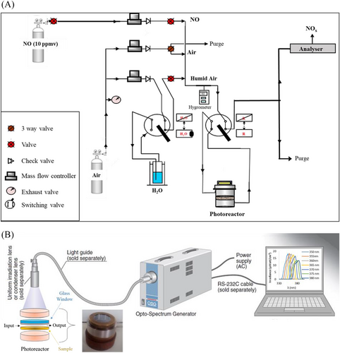
Experiments were performed with a tangential gas flux (600 mL min–1 and initial NO concentration of 200 ppbv), at room temperature, ambient pressure and relative humidity of 40%. The gases used in the experiment, NO 10 ppmv in N2 (99% purity) and compressed air (99.9% purity) were purchased from air liquid. The UV lamp used was the Hamamatsu L12194 Opto-Spectrum Generator (OSG) which emits light at any desired wavelength with high reproducibility by delivering a spectral bandwidth of approximately 20 nm. The used lamp is capable to emit light with an irradiance of 290 μW cm-² at 350 nm and up to 1670 μW cm-² at 400 nm. The wavelength range can be selected and tuned, with a selectivity of 20 nm and steps of 5 nm, in such a way to investigate the influence of the photonic lattices, and in particular optical resonances, on the photochemical processes. The photocatalytic set up is shown in Figure 6. Prior to the photocatalytic treatment, the sample was treated overnight under UV irradiation to degrade all organic impurities existing on the sample and then three steps were followed: at first, pollutant (NO) concentration was stabilized and homogenized by passing the reactor (step 1). Then, it was introduced into the reactor and maintained in the dark until reaching a steady state of pollutant concentration (step 2). Finally, UV light was switched on and maintained until stabilization of the concentration (step 3). All products and intermediates (NO-NO2-NOX) were analyzed continuously using Model 42i (Thermo Scientific), analyzer which is a chemiluminescent device for the continuous and real-time measurement of nitrogen oxides in ambient air.
ACKNOWLEDGMENTS
This work was funded by the IDEXLYON from Université de Lyon, Scientific Breakthrough project IPPON within the Programme Investissements d'Avenir (ANR-16-IDEX-0005). Samples were fabricated in the Nanolyon and NanoSaintEtienne technological facilities, with the support of CNRS-Renatech+ and the FEDER CARAT project (Région Auvergne Rhône-Alpes). FDTD simulations were performed on the Newton computer cluster facilities operated by PMCS2I at Ecole Centrale de Lyon.
CONFLICT OF INTEREST
The authors declare no conflict of interest.
Open Research
DATA AVAILABILITY STATEMENT
The data that support the findings of this study are available from the corresponding author upon reasonable request.


