Ultra-Wideband Terahertz Integrated Polarization Multiplexer
Abstract
Polarization-division multiplexing is crucial for increasing channel capacity and spectral efficiency in communications. A key component is the polarization multiplexer, which combines or separates signals with orthogonal polarizations. Existing planar multiplexers lack an ultrawide band for terahertz communications. While microwave-inspired orthomode transducers (OMTs) provide broadband operation, they suffer from high ohmic loss and bulkiness at terahertz frequencies. Optical integrated polarization beam splitters (PBSs) offer low loss and good integrability but have narrow bandwidths. This work presents a substrateless all-silicon polarization multiplexer based on tapered directional couplers and air-silicon effective mediums, integrated monolithically on a compact footprint. The device demonstrates a 37.8% fractional bandwidth, an average insertion loss of 1 dB, and a polarization extinction ratio above 20 dB over 225–330 GHz. This superior performance is enabled by the anisotropy of the effective medium claddings, affecting the two orthogonal guided modes differently. The multiplexer enables simultaneous two-channel terahertz fiber communications with polarization diversity. It supports aggregated data rates up to 155 and 190 Gbit with bit error rates below hard- and soft-decision forward-error-correction limits, respectively. This advancement holds promise for 6G terahertz integrated systems with enhanced channel capacities.
1 Introduction
All-silicon effective-medium-clad dielectric waveguides together with their peripherals have been demonstrated to be able to route terahertz waves with extremely low dissipation, low dispersion, and broad bandwidth, while supporting two orthogonal fundamental modes namely the mode (with in-plane polarization) and the mode (with out-of-plane polarization).[1, 2] To enable an integrated platform for functional systems, various capabilities for on-chip signal processing must be provided within this framework, such as filtering, modulation, multiplexing, and polarization control.[3] Owing to the controllable relative permittivity of the effective medium, various passive components with different functionalities and high performance have been conceptualized and demonstrated.[2, 4-13]
To manipulate on-chip polarization states, polarization rotators, and multiplexers are indispensable components.[14, 15] In particular, polarization multiplexers able to combine/separate signals with orthogonal polarizations are in demand for many applications especially for communications to achieve increased channel capacities.[15-19] Inspired by microwave technologies, orthomode transducers (OMTs) based on rectangular metallic waveguides have been proposed for terahertz operation.[20-26] Typically, the OMTs are in the form of 3D structures with broad bandwidth and low polarization cross–talk due to the cutoff of the host rectangular waveguides.[24, 26] However, the ohmic loss of the metallic waveguides is significantly increasing with increasing operation frequency[23] and becomes pronounced in the terahertz range. Additionally, the geometrical symmetry required to achieve high performance over a broad bandwidth makes the computer numerical control (CNC) machining or micromachining fabrication more challenging.[25] Simpler OMTs with no symmetrical requirements can relax the fabrication requirements at the cost of a narrower bandwidth and increased cross–talk levels due to the higher-order mode conversion.[23] Nevertheless, the OMTs are still undeniably helpful for communications and radio astronomy with hollow-waveguide-based distributed systems at the cost of fabrication complexity and device integrability.[24]
Unlike in the terahertz domain, integrated polarization multiplexers have been extensively studied in the optical regime, especially for silicon integrated photonics.[14] In general, the optical polarization multiplexers also known as polarization beam splitters (PBSs) can be realized based on various methods including Mach–Zehnder interferometers (MZIs),[27-29] multimode interferometers (MMIs),[30-37] photonic crystals (PCs),[38-41] photonic inverse design,[42] and directional couplers.[43-51] Despite their good integrability and low loss compared to the metallic structures mentioned above, there exists tradeoffs among these conventional optical PBSs in terms of operation bandwidth, insertion loss, structural compactness, and fabrication complexity. In particular, with structural and design simplicity, directional couplers have been widely exploited in the design of optical PBSs. Typically, for such PBSs, a strong polarization birefringence is required to produce a large difference in beat length, which in turn enables a compact footprint together with a high polarization extinction ratio (PER).[14] However, for a conventional silicon-based uniform directional coupler, the polarization birefringence is usually weak leading to an electrically long coupler length and a relatively low PER. Furthermore, due to the coupling being strongly dependent on frequency, the operation bandwidth is narrow, while stringent requirements on the coupler dimensions result in a device performance that is highly sensitive to fabrication tolerances.[14] Recently, an optics-inspired[44] terahertz PBS based on a silicon directional coupler was proposed, which operated over 434–466 GHz with a fractional bandwidth of together with an insertion loss dB and a polarization extinction ratio of dB on a footprint of , where is the wavelength at central frequency.[52] While appreciable, the reported performance limits its applications at terahertz frequencies that entail generous fractional bandwidth. For example, a typical terahertz time-domain spectrometer usually achieves a fractional bandwidth over 60%,[53] while for communications the terahertz band spanning 252.72–321.84 GHz has been channelized for high-speed wireless communications with a fractional bandwidth of 24%.[54]
To further increase the polarization birefringence, and thus the PER of the directional-coupler-based PBS, asymmetric couplers have been widely adopted.[55] This method aims to achieve a specified phase matching condition through cross-coupling over a short coupling length for a given propagating mode, and simultaneously suppressing coupling through phase mismatch for the other mode. In particular, among the reported asymmetric-directional-coupler multiplexers, the performance was improved with assistance of various components, such as bends,[43, 44] slots,[55] gratings,[46, 56] tapered sections,[45] hybrid waveguides,[35, 47-49] and multiple waveguides.[44, 50, 51] However, it remains challenging to simultaneously achieve a broad bandwidth and a high extinction ratio on a compact footprint. Therefore, so far there is no suitable solution scalable from either the microwave or optical domain that can satisfy simultaneous low insertion loss, broad bandwidth, high polarization extinction ratio, and compact footprint.
In this context, a terahertz polarization multiplexer implemented onto the effective-medium-clad all-dielectric waveguide platform is presented in this work. This all-silicon integrated device together with the platform is specially designed for terahertz integration and aimed at the future portable frontends for wireless communications. The proposed multiplexer is based on tapered directional couplers[57-63] that can offer a much broader bandwidth compared to conventional directional couplers, while an anisotropic effective medium is introduced to significantly enhance the polarization birefringence on a single-material platform with a single fabrication process. In this case, the birefringence of the polarization multiplexer is significantly increased leading to a high PER across the broad bandwidth of the tapered coupler. The proposed approach is experimentally validated with a specific design exhibiting a fractional bandwidth of over 225–330 GHz with a measured average insertion loss of 1 dB, and an average PER above 20 dB for the and modes on a modest footprint of .
Here, we would like to emphasize the principle of the proposed ultra-wideband polarization multiplexer. In our design, the significant birefringence is achieved by the in-plane anisotropic effective medium claddings, fundamentally different from the asymmetric waveguides that were widely used by optical directional-coupler-based polarization beam splitters, including the subwavelength-grating-waveguide-based beam splitters.[46, 56, 64, 65] Our rationale of this design is that, unlike asymmetric waveguide designs, anisotropic claddings are only mildly frequency dependent. As a result, the broad bandwidth available from the tapered coupler is fully utilized with the introduction of effective medium claddings, yielding a fractional bandwidth of nearly 40%. This is in stark contrast with the existing optical designs, where the generous bandwidth offered by tapered couplers is largely under utilized due to the limitation of PER, which usually leads to a fractional bandwidth of only a few percents.[66] The maximum reported bandwidth is 28% but with the PER limited to 10 dB,[56] compared with 37.8% and 20 dB in our case. While structures like subwavelength grating (SWG) waveguides can be introduced to enhance the PER bandwidth,[46] the improvement is still unmatched by the vast available bandwidth of the tapered coupler.[57, 58]
2 Design Concepts
2.1 Overview
As shown in Figure 1a, the proposed polarization multiplexer is built on the effective-medium-clad dielectric waveguide platform to achieve high efficiency, broad bandwidth, and high PER. The entire structure is based on a 250--thick high-resistivity float-zone silicon wafer with a relative permittivity of , loss tangent of , and resistivity larger than . The waveguide widths are selected for supporting only the fundamental mode of each polarization. The effective medium claddings are realized by periodically perforating the silicon slab with deep subwavelength spacings,[1, 2] where the claddings are formed in hexagonal lattices to enhance the mechanical strength as shown in Figure 1b,c. To better conceptualize the design, the multiplexer clad by artificial homogeneous materials is shown in Figure 1d. The multiplexer is designed to split the two fundamental modes with orthogonal polarizations, i.e., the mode with in-plane polarization and the mode with out-of-plane polarization, into two paths, as illustrated in Figure 1a. Segments of regular waveguides cladded by lower-index effective medium claddings are used to interface with feeding tapers and the polarization multiplexer for a consistent interconnection with other components on the same platform.[4]
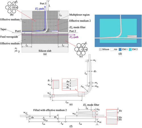
The proposed polarization multiplexer can be understood by considering separately two paths namely the -path and the -path as shown in Figure 1e,f. The -path includes two tapered directional couplers connected by a sharp bend. Here, the tapered directional couplers can achieve a much broader bandwidth compared to the conventional uniform directional couplers. Importantly, the effective medium claddings surrounding the couplers are systematically designed so as to achieve a sufficiently high PER. For each coupler, the two evanescently coupled waveguides are laterally tapered and inversely positioned with a small coupling air gap along a sufficiently long coupling length. Such a design aims to achieve a high power transfer for the mode while rejecting the mode over the operation frequency range from 220 to 330 GHz (WR-3.4 band). In this case, the configuration with double couplers enhances the performance by increasing the polarization extinction ratio. Introducing more couplers can further increase the PER but at the expense of higher complexity and coupling loss. Alternatively, the PER can also be improved by optimizing the effective medium claddings of the second coupler while keeping a low insertion loss and a compact footprint compared to the conventional multiple cascaded structures. A sharp bend with low bending loss[67, 68] is adopted to reduce the device footprint while minimizing the interferences with the -path. The claddings surrounding the bend are based on the principles discussed in Ref. [2], where radially arranged elliptical hole arrays are adopted to maintain an identical effective refractive index in both inner and outer claddings.
The -path consists of two symmetric tapered waveguides bridged by a thin straight waveguide with a relatively wide coupling gap as shown in Figure 1f. To minimize the interference with the -path, the two tapered waveguides are isolated with a certain distance. The bridging waveguide aids the coupling between the two tapered sections for the mode. Typically, due to a larger in-plane field penetration depth of the mode,[2, 69] a combination of a wider coupling gap and a higher refractive index of filling material can support a high transmission for the mode with a low transmission level for the mode. Here, the effective medium with a tailorable refractive index is therefore crucial to the performance. Additionally, the core width of the bridging waveguide should be narrow so as to provide a good mode matching over a broad bandwidth for the gradually leaked mode from the tapered waveguide. To further enhance the PER, an mode filter consisting of multiple tapered sections is introduced as shown in Figure 1f, so that the remaining power in the mode is trapped in the filter while the mode can pass through with a negligible impact. The mode filter leverages the identical principle adopted in the -path design relying on the polarization dependence of the tapered couplers. It is noteworthy that as shown in Figure 1a, additional effective-medium claddings are introduced outside the polarization multiplexer region with a lower relative permittivity compared to the one in the polarization multiplexer region. This index contrast between the two regions is designed to minimize the leakage into the nearby silicon slab.
2.2 Effective-Medium-Clad Tapered Directional Couplers
The tapered directional couplers play an important role in achieving polarization differentiation in the proposed polarization multiplexer concept. Generally, a tapered directional coupler can be realized by tapering the geometries of the guiding structures and/or the refractive indices of the surrounding materials.[57-63] As a result, the tapered couplers can operate in the evanescent coupling regions without even and odd mode interference or critical beat length involved. For a tapered directional coupler, the quasi-even (in-phase) and quasi-odd (out-of-phase) modes, both having an asymmetric mode profile in the two coupled lines, co-exist due to the waveguides tapering. Notably, it is possible to allow only one of the quasi-modes to be excited with all its power concentrated in one waveguide at the beginning and in the other waveguide at the end.[58] Free of mode interference, the tapered coupler can achieve a much broader bandwidth than the uniform coupler. It is noteworthy that based on the coupled mode theory the bandwidth of a tapered coupler is affected by the cross–talk between the quasi-even and quasi-odd modes, which degrades the coupling efficiency of the coupler. Such a mode cross–talk is measured by , where is a function of the variation of the propagation constant difference between the two coupled lines and their coupling coefficient , while is the function of the beat wavelength .[58] Since, in general, and are dependent on frequency, the mode cross–talk is also frequency dependent. Therefore, the frequency range with the mode cross–talk level less than a certain threshold determines the bandwidth. Mathematically, the mode cross–talk can be reduced to zero if all derivatives vanish thus leading to an infinite bandwidth.[58] In other words, must be varied slowly compared to . Physically, a broader bandwidth can be achieved by gradually tapering the waveguide with a longer coupler length.[58]
Here, we show that how a combination between the tapered coupler and effective medium can significantly enhance the polarization discrimination with great design flexibility. Specifically, given a laterally tapered waveguide, the derivative of the propagation constant is mainly determined by its lateral component, , which is a function of the waveguide width and the in-plane claddings. Given a linearly tapered waveguide with a constant slope, the varying rate caused by the tapering waveguide width is identical for the two orthogonal polarizations. Therefore, the distinctive terms for the derivative of the propagation constant between two polarizations are the effective refractive indices. The anisotropy of the effective medium[70] results in distinctive for the two modes. Specifically, the propagation constant variation for the mode is smaller than that of the mode, resulting in a higher power transfer. The specific mathematical proof can be found in the Supporting Information, which demonstrates how the anisotropy of the effective medium claddings affects differently for both components. Since the anisotropic refractive indexes are virtually frequency independent, such a mechanism can maintain the ultra-wide bandwidth of the tapered coupler while achieving a high PER and a reasonably compact footprint. The in-depth analysis provides insight into the design principles underpinning the superior performance of the proposed polarization multiplexer. This mechanism does not exist in the silicon-on-insulator platforms with isotropic claddings.
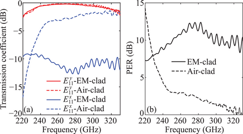
Taking a tapered directional coupler as an example, an optimal effective-medium cladding relative permittivity tensor has been obtained through simulations as resulting from a hole array configuration with (100 , 80 ). As shown in Figure 2, this cladding configuration can achieve an average transmission level of dB for the mode and dB for the mode, leading to an average PER 10 dB over the frequency range from 220 to 330 GHz. On the contrary, an air-clad coupler shows a comparable average transmission level for the mode and dB for the mode, resulting in an average PER of merely 3 dB. The higher PER at lower frequencies for the air-clad tapered coupler in Figure 2 is mainly because the mode has a lower transmission due to a weaker wave confinement than an EM-clad one. This effect is not desirable as it reduces the efficiency of the port. In this sense, compared to the case with air claddings, the designed effective medium claddings can provide an enhanced PER over a broad bandwidth. A more general case study that further proves the concept together with the evolution of the proposed design from effective-medium-clad tapered couplers can be found in the Supporting Information.
3 Results and Discussion
3.1 Realized Effective-Medium-Clad Polarization Multiplexer
The realized substrateless all-silicon effective-medium-clad polarization multiplexer is shown in Figure 3. As illustrated in Figure 4a,b, the measured results agree well with simulations, while the slight discrepancies between the measurement and the simulation are mainly due to the fabrication tolerances and sample misalignment in the measurements. Specifically, sample shift and/or rotation with respect to the feeding hollow waveguides can cause significant fluctuations in the transmission coefficients and/or polarization cross–talk.[2] This is due to the modal difference between the metallic waveguide feed and the dielectric waveguide. Additionally, evanescent fields of the effective-medium-clad waveguide is another cause, i.e., the mode with weaker wave confinement with a larger evanescent field penetration into the claddings is more sensitive to misalignment.[2] The degraded measured transmission level for the mode at the lower frequencies as shown in Figure 4b is mainly because of the observed reduced wafer thickness from to as shown in Figure 3d, leading to weaker wave confinement of the waveguide especially at lower frequencies for the mode.[2] The thickness decrement is slightly larger than the fabrication tolerance of the silicon wafer that is as quoted by the manufacturer. Such an effect has been verified through simulations. The measured PER for the mode is above 18.5 dB with an average value of 26.1 dB, while it is above 16 dB with an average value of 24.3 dB for the mode over 220–330 GHz, as shown in Figure 4c,d. The decrement in transmission of the mode is not expected to impact the overall performance in a consequential manner considering the average PER above 20 dB for both polarizations. One straightforward way to further improve the PER of the polarization multiplexer is to adopt cascaded couplers at the expense of an increased device footprint. Instead, the PER can be further enhanced by optimizing the effective medium claddings surrounding the second tapered coupler along the -path.
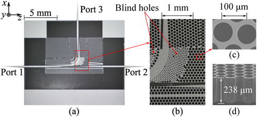
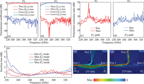
The insertion loss is calibrated by comparing the transmission coefficients of straight waveguides and the multiplexer. Nonetheless, this calibration process cannot completely remove the effect of sample misalignment due to alignment uncertainties across different samples. As shown in Figure 4e, the measured insertion loss for the mode is below 2 dB with an average of 0.9 dB across the whole operation frequency range, which agrees well with the simulation. For the mode, the measured insertion loss is below 5.2 dB, which decreases with increasing frequency and converges to the simulation, leading to an average loss of 1 dB over 220–330 GHz. The insertion loss for the mode can be further improved by increasing the bending radius without changing other characteristics.
The simulated -field distributions for the and modes at the central operation frequency, i.e., at 275 GHz are shown in Figure 4f,g. As shown in Figure 4f, for the mode, the waves can be transmitted well through the bridge, while the waves coupled to the -path are leaked into the claddings at the second tapered coupler leading to a low cross–talk level in the -path. At the mode filter near to the exit of the -path, there is a small portion of waves coupled to the air slots. The thin bridging waveguide experiences mild wave leakage. These effects together can lead to slightly reduced transmission level of the mode. To increase the bandwidth and reduce the insertion loss, the mode filter design along the -path can be further optimized to suppress the higher-order mode excitation at higher operation frequencies caused by the waveguide discontinuities. For the mode, as shown in Figure 4g, most of the power can be transmitted through the tapered couplers with a small portion of power leaking to the -path and trapped by the mode filter eventually.
3.2 Communications Demonstration
To demonstrate that the proposed polarization multiplexer is able to double the communication channel capacity, simultaneous two-channel real-time HD-video transmission at 300 GHz is performed with the experimental setup shown in Figure 5. On the transmitter side, two tunable near-infrared laser sources are adopted to generate an optical beat signal with a frequency difference of 100 GHz as illustrated in Figure 5a. Amplified by the EDFA, the optical beat signal is divided into two channels by a 3-dB optical power divider, and modulated with a HD-video signal generated by a video player in each channel. The amplified modulated beat signal is injected into a UTC-PD and downconverted to a signal at 100 GHz, which is amplified and upconverted to 300 GHz by an amplifier and a multiplier. Such a UTC-PD setup allows to achieve reasonable signal-to-noise ratio at the receiver given the link budget. The terahertz signal in each channel is coupled to the multiplexer through a WR-3 hollow waveguide, while the polarization diversity is obtained by rotating the orientations of the hollow waveguides. The two terahertz signals with orthogonal polarizations carrying two different data streams are combined by our polarization multiplexer and coupled to a terahertz hollow-core fiber, which can support two orthogonal polarizations over a broad bandwidth.[71] The simulated coupling loss between the tapering structure and the fiber is dB for the mode and dB for the mode. Due to the diameter of the hollow fiber (1 mm) much larger than the taper end, the taper structure can be easily inserted into the fiber without touching the walls. The reasons to adopt the fiber as an interconnect are to avoid the significant propagation path loss and to simplify the setup and alignment compared to the free-space transmission with lenses and/or mirrors introduced.

On the receiver side, another sample working as a demultiplexer coupled to the fiber is introduced to separate the two signals with orthogonal polarizations into two different paths, where SBDs are used to retrieve the modulating data from the received terahertz signals. Amplified by the LNAs, the HD-videos are displayed on the video displays and the demonstration can be found in visualization of Supporting Information. While the data rate for each channel is limited to 1.5 Gbit , the uncompressed HD-video transmission requires a bit error rate of or less with no online/offline signal post-processing, so video quality is extremely sensitive to the device insertion loss, dispersion, and especially polarization cross–talk. We believe that the real-time video transmission demonstration is the ultimate proof that our device is working perfectly as designed. The proposed polarization multiplexer is expected to support a much higher data rate considering its low loss, low dispersion, high PER, and good port isolation over a broad bandwidth. The details of the dispersion characteristics and port isolation can be found in the Supporting Information.
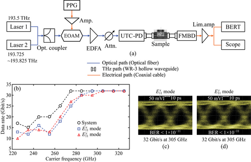
To demonstrate the capacity of the proposed polarization multiplexer in terahertz communications, we perform experiments for high-speed data transmission with on–off keying (OOK) and 16-QAM modulations. The setup for OOK transmission is shown in Figure 6a, where the terahertz signals are generated based on the optical heterodyne method through a UTC-PD, similar to the one for a single channel in HD-video transmission shown in Figure 5a. At the transmitter side, a pulse pattern generator is used to modulate the optical beat signals. At the receiver side, a Fermi-level managed barrier diode (FMBD) receiver that is integrated with a trans-impedance amplifier and has a high sensitivity and broad bandwidth[72] is adopted to down-convert the terahertz signals to baseband frequency. A bit error rate tester (BERT) is used to measure the bit error rate (BER), while the eye diagrams are measured by an oscilloscope. As shown in Figure 6b, limited by the capacity of the system, the highest data rate for both polarizations can reach 32 Gbit with a BER below , leading to a maximum error-free aggregated data rate of 64 Gbit . Eye diagrams with clear openings for error-free transmission at 305 GHz are shown in Figure 6c,d. It is noted that the discrepancies in the transmission data rate between the device and the system at lower carrier frequencies are mainly caused by the coupling loss between the sample and the hollow waveguides. The coupling loss is gradually improved with operation frequency increasing due to better wave confinement in the dielectric waveguide. The slight discrepancy between the mode and the mode is mostly caused by the alignment issue, where some unexpected reflections can occur, leading to variations in the signal-to-noise ratio (SNR).
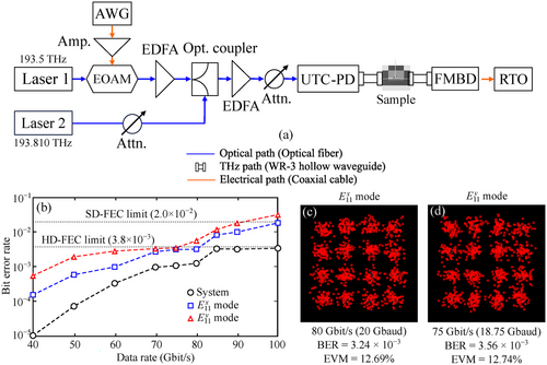
To achieve a higher transmission data rate, intermediate frequency (IF) transmission at the carrier frequency of 310 GHz with 16-QAM modulation is conducted with the setup shown in Figure 7a, where an arbitrary wave generator (AWG) and a real-time oscilloscope (RTO) are used to generate and demodulate the digital signals, respectively. An optical variable attenuator controls the pilot signal to optimize the carrier-to-noise ratio of the optical beat signals. Here, the IF frequency is chosen as 12 GHz and the output power of the UTC-PD is −12 dBm (photocurrent: 6.5 mA). As shown in Figure 7b, the BER increases with the data rate increasing and approaches the hard decision forward error correction (HD-FEC) limit with an overhead of 7% (BER = ). As a result, a maximum data rate of 80 Gbit (20 Gbaud) for the mode and 75 Gbit (18.75 Gbaud) for the mode are achieved with the constellation diagrams shown in Figure 7c,d, leading to a maximum aggregated data rate of 155 Gbit . Additionally, a maximum aggregated data rate of 190 Gbit is confirmed for the SD-FEC threshold (BER = ). Such a data rate is reasonable considering the coupling loss and the 3-dB bandwidth of the device. For the IF transmission with 16-QAM modulation, a 3-dB bandwidth of 28–32 GHz and a minimum SNR of 15 dB are typically required to support a baud rate of 20 Gbaud with a BER below the HD-FEC limit, which corresponds to the results with OOK transmission shown in Figure 6b. Compared to the system performance, the degraded BER of the device is mainly because of the coupling loss between the sample and the hollow waveguides, while the slight discrepancies between the mode and the mode may be attributed to the slight difference in the dispersion characteristics discussed in the Supporting Information. Although the aggregated data rate might be slightly reduced for the simultaneous transmission due to the interference of the polarization cross–talk, these results further demonstrate the device's potential in supporting high-speed on-chip data transmission with a data rate over 100 Gbit .
3.3 Discussion
A comparison of various polarization multiplexers at optical and terahertz frequencies is shown in Table 2. Here, we listed the average insertion loss rather than the worst insertion loss. This is to avoid fluctuations in the measured insertion loss due to fabrication and measurement imperfections. Additionally, we define the bandwidth of our device with measured 20 dB to maintain a high signal-to-interference ratio for high-speed communications. Therefore, the operation frequency range satisfying this figure of merit is reduced to 225–330 GHz with a fractional bandwidth of 37.8%. Compared to the microwave-inspired orthormode transducers (OMTs), the proposed polarization multiplexer has good integrability, comparable broad bandwidth, and insertion loss. In particular, the proposed multiplexer has a much simpler structure and lower fabrication complexity compared to the turnstile OMT operating at the WR-3.4 band.[25] Since the proposed terahertz all-silicon polarization multiplexer is designed based on photonic methods and scalable to optical frequencies, comparing the performance with optical PBSs is feasible. To ensure a fair comparison in terms of bandwidth, we adopt as a performance measure the fractional (normalized) bandwidth, defined as the absolute bandwidth divided by the center frequency. Among the integrated optical PBSs, the proposed design has a much broader bandwidth together with a low insertion loss (IL), high PER, and a competitive footprint. While the measured fractional bandwidth of the proposed design is reduced to 37.8% due to fabrication tolerances, the resulting absolute bandwidth would be 554.7 nm if it were to be scaled to 1467.5 nm (center frequency of the optical communications bands). Such a bandwidth could cover all the optical communications bands including O-, E-, S-, C-, L-, and U-bands. Despite a similar PER and an insertion loss, the proposed polarization multiplexer can achieve a more than twofold bandwidth on a much more compact footprint compared to the waveguide-coupler-based optical PBS.[46] By leveraging the anisotropy of the effective medium claddings to enhance the inherent birefringence of the tapered directional coupler, the proposed design notably outperforms the optical PBSs adopting subwavelength grating (SWG) waveguides.[64, 65] While the SWG waveguide-based PBSs also leverage the concept of effective medium to engineer the waveguide modal indices,[73, 74] their design principle is similar with that of the work leveraging the asymmetric waveguides to achieve different phase match conditions for the two orthogonal polarizations. Therefore, the bandwidth is mainly limited by the dispersion of the waveguides. It is noted that the dispersion in the SWG waveguide is strong and requires a high duty cycle to be flattened, which in turn increases fabrication difficulties.[64, 65, 73, 74] One most representative SWG waveguide-based optical PBS can be found in Ref. [65], showing a fractional bandwidth of with a PER > 20 dB. Although the SWG-slot-waveguide-based PBS shows a larger bandwidth,[56] the low PER limited its applications especially, in communications, where a PER > 20 dB is critical to achieve a high signal-to-interference ratio that allows for a high transmission data rate. Terahertz-integrated polarization multiplexers are emerging, and most of the existing designs were downscaled from the optical domain. These scaled versions possess a few percent of fractional bandwidths and large footprint,[75, 76] which are not practical for terahertz applications, e.g., portable communications frontends. For example, compared to the terahertz PBS in Ref. [52], the proposed polarization multiplexer has a bandwidth that is more than five times as broad, with superior insertion loss and PER. Furthermore, owing to the effective medium increasing the polarization birefringence, the proposed design has a more than three times smaller footprint compared to Ref. [52], which proposed a silicon terahertz polarization splitter cladded by air.
| [] | [] | [] | [] | [] | [) | [] | [] | [] |
| 100 | 90 | 80 | 20 | 75 | 70 | 140 | 252.5 | 20 |
| [] | [] | [] | [] | [] | [) | [] | [] | [] |
| 112.5 | 3000 | 3000 | 2500 | 3500 | 800 | 2000 | 2800 | 1000 |
| [] | [] | [] | [] | [] | [) | [] | [] | [] |
| 225 | 225 | 87.5 | 205 | 205 | 225 | 700 | 300 | 95 |
| Frequency [THz] | Bandwidtha) | PER [dB] | Average IL [dB] | Footprintb) | |
|---|---|---|---|---|---|
| () | () | ||||
| Microwave-inspired OMT | |||||
| Asymmetrical OMT[23] | 0.500–0.600 | 18.2% | >20 (>20) | 2.5 (2.5) | 3D |
| Turnstile OMT[25] | 0.220–0.330 | 40.0% | (>30) | 0.3 (0.3) | 3D |
| Double-ridged waveguide OMT[26] | 0.275–0.500 | 58.0% | (>30) | 1.0 (1.0) | 3D |
| Optical PBS | |||||
| Photonic inverse design[42] | 191.57–195.57 | 2.1% | >10 (>10) | 1.5 (1.5) | |
| MMI-based[34] | 190.48–196.72 | 3.2% | >15 (>15) | 0.8 (1.7) | |
| PC-based[40] | 187.02–196.61 | 5.0% | (>10) | 5.6 (4.6) | |
| MZI-based[29] | 188.09–199.34 | 5.8% | >10 (>10) | 0.5 (0.5) | |
| Directional-coupler-based | |||||
| Hybrid-plasmonic-waveguide coupler[48] | 191.69–196.08 | 2.3% | >15 (>15) | 1.5 (1.5) | |
| Hybrid-dielectric-waveguide coupler[47] | 190.47–195.44 | 2.6% | >20 (>20) | 0.4 (0.15) | |
| Triple-bent-waveguide coupler[44] | 186.34–197.37 | 5.8% | >20 (>20) | 0.6 (0.3) | |
| Tapered-waveguide coupler[66] | 185.19–197.37 | 6.4% | >15 (>15) | 0.4 (0.4) | |
| Multimode-tapered-waveguide coupler[50] | 185.19–197.37 | 6.4% | >15 (>15) | 3.5 (6.75) | |
| Bent-waveguide coupler[43] | 186.34–203.39 | 8.8% | >20 (>20) | 1.0 (1.0) | |
| Bent-slot-waveguide coupler[55] | 184.05–204.08 | 10.3% | >10 (>10) | 0.3 (0.3) | |
| SWG-waveguide coupler[65] | 179.1–205.48 | 13.7% | >20 (>20) | 1.0 (1.0) | |
| Grating-waveguide coupler[46] | 181.26–209.06 | 15.6% | >20 (>20) | 1.0 (1.0) | |
| Grating-slot-waveguide couple[56] | 178.57.93–238.1 | 28.6% | >10 (>10) | 1.0 (1.0) | |
| Terahertz PBS | |||||
| MMI (Sim. only)[75] | 6.4–6.5 | 1.6% | >22 (>22) | 2 (2) | |
| Photonic crystal & MMI (Sim. only)[76] | 1.86–1.96 | 2.5% | >13 (>13) | 2.23 (2.02) | |
| Asymmetric directional coupler[52] | 0.433–0.466 | 7.1% | >10 (>10) | 3.7 (3.7) | |
| This work | 0.225–0.330 | 37.8% | >20 (>20) | 1.0 (1.0) |
- a) The bandwidth is defined based on the claimed minimum polarization extinction ratio (PER).
- b) The footprint for the OMT block is mainly determined by the flange size of the rectangular waveguide.
4 Conclusion
In conclusion, we have presented a terahertz polarization multiplexer based on an effective-medium-clad waveguide platform over the frequency range from 220 to 330 GHz. The proposed multiplexer has been experimentally validated with a 20-dB PER fractional bandwidth of nearly with an average insertion loss of 1 dB on a compact footprint of . The thorough analysis shows that the combination of the tapered directional coupler and the effective medium can achieve high-performance polarization multiplexing in terms of bandwidth and polarization extinction ratio. In particular, the effective medium platform yields high design flexibility including for its effective anisotropy, which is essential for polarization control. The nearly fractional bandwidth of the proposed polarization multiplexer is 20 times as wide as that of the optical C-band. This is much needed for terahertz applications especially for 6G and beyond communications with increased channel capacities. Such a concept has been demonstrated through high-speed on-chip communications and simultaneous two-channel HD-video transmissions with manageable polarization cross–talks. Considering scalability, the proposed concepts can benefit integrated photonics at large.
5 Experimental Section
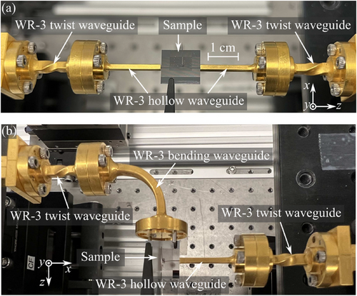
The fabrication of the proposed polarization multiplexer was based on a deep reactive-ion etching (DRIE) process with a 250- high-resistivity (>10 ) intrinsic float-zone silicon wafer. The specific fabrication process was as follows. First, photoresist (AZP-4620, MicroChemicals GmbH, Germany) was spin-coated on the silicon substrate and then patterned by photolithography. The patterned photoresist acted as an etching mask material for protection during the DRIE process. Then, a DRIE instrument (MUC-21 ASE-SRE, SPP Technologies Co., Japan) was employed to remove the silicon perpendicularly from the front to the back side of the substrate through the ionized gas. Lastly, the remaining photoresist was removed using acetone and oxygen ashing (RIE-10N, SUMCO Co., Japan). The fabrication accuracy was closely related to the aspect ratio between the wafer thickness and hole diameter for the deep reactive ion etching process. The feasible aspect ratio for the facilities employed in this work was 10:1. In this case, the required minimum diameter of the holes that could be etched through was 25 , given the wafer thickness of 250 . The hole size and tapered directional couplers could be precisely defined through photolithography, at least on the topmost part, as photolithography was good down to sub-micron accuracy. However, the issue was the vertical tapering of the hole as the aspect ratio increased. Despite some imperfections like tapered holes and blind holes in the claddings, the device's high performance remained, showing the robustness of effective medium. The full-wave simulation was performed with CST Microwave Studio 2023. The scattering parameters measurements were conducted by using a Keysight vector network analyzer (VNA) with VDI WR-3.4 extension modules spanning from 220–330 GHz as shown in Figure 8.
Acknowledgements
This work was supported by the Australian Research Council Discovery Project under Grant No. ARC DP180103561. Part of this research result was obtained from the commissioned research (No.00901) by National Institute of Information and Communications Technology (NICT), Japan, and the Core Research for Evolutional Science and Technology (CREST) program of the Japan Science and Technology Agency (No. JPMJCR21C4). The authors acknowledge Dr. M. Li, Dr. N. Ngo, Mr. D. Ichikawa, and Dr. R. Koala for their assistance in the experiments.
Open access publishing facilitated by The University of Adelaide, as part of the Wiley - The University of Adelaide agreement via the Council of Australian University Librarians.
Conflict of Interest
The authors declare no conflict of interest.
Open Research
Data Availability Statement
The data that support the findings of this study are available from the corresponding author upon reasonable request.


