Surface Acoustic Microwave Photonic Filters on Etchless Lithium Niobate Integrated Platform
Abstract
Lithium niobate on insulator emerges as a promising platform for integrated microwave photonics because of its capability of ultralow-loss guidance and high-efficiency modulation of light. Chip-level integration of microwave filters is important for signal processing in the 5G/6G wireless communication. Here, by employing bound states in the continuum for low-loss waveguiding, high-performance microwave photonic filters are realized on an etchless lithium niobate integrated platform. These microwave photonic filters consist of a high-quality photonic microcavity modulated by piezoelectrically excited surface acoustic waves. Acoustic time delays from 21 to 106 ns and passbands with bandwidth as narrow as 0.89 MHz are achieved in the fabricated filters operating at gigahertz frequencies. This demonstration may open up new applications on the lithium niobate integrated platform, such as optical communication, signal processing, and beam steering.
1 Introduction
Integrated microwave photonics (MWP) by combining photonic integrated circuit technology with MWP has shown its advantages in enhanced functionalities and robustness as well as reduced size, weight, cost, and power consumption. Microwave filtering is one of the most important functionalities in integrated MWP for signal processing in the 5G/6G wireless communication,[1, 2] which separates signals of interest from the noise background and mitigates unwanted interference.[3] A common way for implementing integrated MWP filters is constructing multitap delay lines on a chip,[4-6] where the input signal is discretely sampled, delayed, and weighted before being summed up. For applications that require narrow linewidths and/or free spectral ranges (FSRs), long time delays become necessary, leading to large footprints and high losses. Hypersonic acoustic waves with significantly lower velocity than optical waves can be adopted for overcoming this difficulty and obtaining the required long time delays within a small footprint. One way of harnessing the acoustic waves for high-resolution filtering relies on the stimulated Brillouin scattering between guided light and sound waves, usually in nonsuspended chalcogenide glasses[7, 8] or suspended silicon membranes.[9-11] Another type of sound waves, surface acoustic waves (SAWs) propagate at the surface of a material within a depth on the order of acoustic wavelength. SAWs have very high energy confinement and can attain large overlap with the optical mode of a planar waveguide on integrated platform, and thus have been widely applied in the areas of quantum communication,[12] sensing,[13, 14] and signal processing.[15-17] More importantly, tunable SAW devices have been achieved recently by using mechanical nonlinear deformations,[18] piezoelectrically actuated deformations,[19] electroacoustic effects,[20] and thermoacoustic effects[21] at gigahertz frequencies. Therefore, SAW devices are an excellent candidate for high-resolution tunable MWP filters for next-generation wireless communication.
To date, most of the integrated MWP components are realized on mature material platforms including indium phosphide,[22-24] silicon on insulator,[16, 17, 25] and silicon nitride on insulator.[26-28] Lithium niobate on insulator (LNOI) emerged as a new and promising platform for MWP due to the advantages of ultrabroad optical transparency window (350–5200 nm), strong piezoelectric effect, and large second-order optical nonlinearity.[29, 30] Moreover, the state-of-the-art lithium niobate integrated photonics technology supports ultralow-loss light propagation, thus enabling high-performance nonlinear applications in a wide wavelength range. All these advantages will lead to lower energy consumption, more compact footprint, and higher integration scale required for the next-generation optoelectronic chips, which pave the way for the 5G/6G communication. Photonic integrated circuits fabricated with etching processes rely on the development of etching recipes to achieve smooth vertical etched sidewalls, which are not yet available for many optical functional materials. Here, we adopted a fundamentally new photonic architecture by patterning a fabrication-friendly optically transparent material on a thin-film substrate without etching the substrate.[31, 32] This architecture features easy fabrication processes and excellent device performance, and has enabled various photonic functionalities on the LNOI platform, including 2D-material integration,[33, 34] high-dimensional communication,[35] and second-harmonic generation,[36] with performance comparable with those fabricated by etching the lithium niobate. Moreover, due to the very different acoustic properties between polymer and lithium niobate, the SAWs can propagate in the unetched lithium niobate layer across the optical waveguides with negligible reflection or scattering, which is ideal for acousto-optic modulation.[37, 38] Here, by monolithically integrating an interdigital transducer (IDT) with a multitap photonic microcavity, we demonstrated high-resolution MWP filters on an etchless LNOI integrated platform for signal processing. The demonstrated filters can be scaled for operation in a wide frequency range from megahertz to tens of gigahertz, which will contribute to the development of high-performance MWP systems on the lithium niobate integrated platform.
2 Results and Discussion

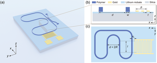
A major motivation for the MWP development is the low-loss transmission over long distances. The optical loss can have considerable effects on the system's performance, because it transforms into the microwave loss quadratically due to the square law in optical-to-electrical conversion by photodetectors.[40] Therefore, low-loss photonic integrated circuits are the foundation for constructing high-performance MWP filters on a chip. For a waveguide structure made of a low-refractive-index material on a high-reflective-index substrate as shown in Figure 1b, the TM-polarized bound mode lies in the TE-polarized continuous spectrum. Therefore, the TM bound mode can interact with the TE continuum, resulting in energy dissipation of the former. However, one can engineer the waveguide geometry to turn the TM bound mode into a bound state in the continuum (BIC) with completely eliminated energy dissipation.[31] To obtain a high-quality photonic microcavity with multiple taps as shown in Figure 1a, one should minimize the waveguide propagation loss in all the straight and bent sections. The upper panel of Figure 2a shows that the propagation loss of the fundamental TM mode in a straight waveguide depends on the waveguide width w. A zero propagation loss can be achieved at w = 1.74 µm at the wavelength of 1510 nm. On the other hand, the propagation loss of the fundamental TM mode in a bent waveguide depends on both the waveguide width w and the bend radius R. The lower panel of Figure 2a plots the simulated propagation loss of the TM mode in a bent waveguide as a function of the bend radius R with w = 1.74 µm. When R > 60 µm, a zero propagation loss can be obtained at periodic R values (R = 78, 92, 106 µm …). Figure 2b shows the modal profiles of the fundamental TM mode in a straight waveguide (upper) and a bent waveguide (lower) at the BIC and off-BIC points marked in Figure 2a. For the TM mode at the off-BIC point, there is obvious energy dissipation to the TE continuum. By contrast, the TM mode at the BIC point exhibits perfectly localized field, resulting in lossless propagation of photons in the continuum.

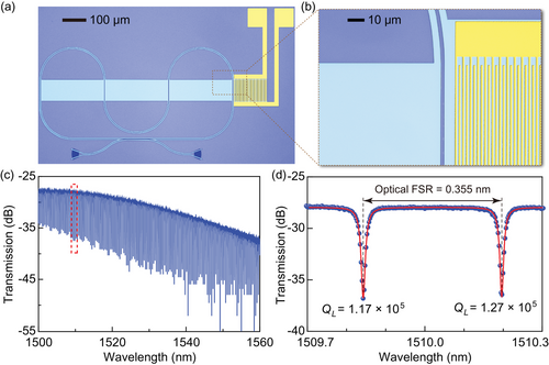
Based on the simulated results, we designed the multitap photonic microcavity by satisfying the BIC conditions for both straight and bent waveguides (w = 1.74 µm, R = 134 µm). The nearby IDT had p = 2w = 3.48 µm unless otherwise noted, to achieve maximal acousto-optic modulation efficiency. We fabricated the devices with an etchless process on a z-cut LNOI substrate. First, the IDT was fabricated with a lift-off process, which involved pattern definition by high-resolution electron-beam lithography and the subsequent gold deposition by electron-beam evaporation. Then, the polymer waveguides and microcavity were fabricated with a second step of electron-beam lithography. Note that in this step the polymer on the SAWs' propagation path was also removed to avoid its possible attenuation effects on the SAWs. Figure 3a shows a top-view optical microscope image of a fabricated 4-tap device, and Figure 3b is a close-up view of its acousto-optic modulation region. We first measured the optical transmission of the photonic microcavity by coupling light into and out of the device via grating couplers. The input light was provided by a tunable semiconductor laser (Yenista T100S-HP) and the output light was collected by a photodetector (Hewlett Packard 81531A). Figure 3c plots the optical transmission spectrum of the device shown in Figure 3a. The zoomed-in spectrum in Figure 3d indicates loaded quality factors QL of ≈1.2 × 10⁵ near the wavelength of 1510.0 nm. The factors preventing attainment of an even higher experimental QL may include waveguide sidewall roughness, material absorption, modal mismatch between the straight and bent sections of the microcavity, and waveguide deformation near the IDT.[41] The QL can be further enhanced by optimizing the fabrication processes. For example, the waveguide sidewall roughness can be reduced by adding a baking step after lithographic patterning of the polymer. The material absorption can be reduced by replacing the polymer with another optically transparent material such as silicon oxide. The waveguide deformation near the IDT can be reduced by inverse compensation during the structural design. The measured optical FSR is 0.355 nm, which agrees well with the theoretical value of 0.358 nm obtained by using the cavity circumference of 2820 µm and the simulated group index of 2.253.

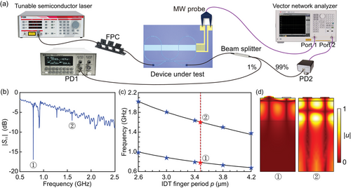
Figure 4a shows the experimental setup for characterizing microwave filtering of the fabricated devices. Light from the tunable semiconductor laser had its polarization adjusted by a fiber polarization controller before being coupled into the device via the input grating coupler. The laser wavelength was tuned to a maximal slope of the photonic microcavity's transmission spectrum. Meanwhile, a sinusoidal microwave signal from a vector network analyzer (Keysight E5071C) was delivered to the IDT via a microwave probe. The light inside the photonic microcavity experienced multiple times of acousto-optic modulation and was strongly enhanced near a cavity resonant wavelength. The light coupled out of the output grating coupler was split and collected by two photodetectors. A high-sensitivity photodetector (Hewlett Packard 81531A) was used to monitor the cavity transmission for tuning the laser wavelength. A high-speed photodetector (Optilab A1803) was used to convert the SAW-modulated light signals into the electrical domain, which were sent back to the vector network analyzer for obtaining the transfer function.

In Figure 4b, the measured |S11| spectrum shows several dips. To identify the excited SAW modes, we fabricated a series of devices with IDT finger period p varying from 2.6 to 4.2 µm. Figure 4c shows the simulated and measured frequencies of the SAW modes, which agree well with each other. The red dashed line marks the case in Figure 4b, where the IDT finger period is p = 2w = 3.48 µm, and the two red stars represent the measured frequencies at the two dips [0.78 GHz (①) and 1.60 GHz (②)]. Figure 4d shows the cross-sectional displacement field profiles (x component) of the two SAW modes. Based on the relationship between the IDT finger period and the excited SAW frequency in Figure 4c, we obtained the simulated velocity of SAW modes ① and ② as ʋ1 = 2714 m s−1 and ʋ2 = 5398 m s−1, respectively (see Section S2, Supporting Information).
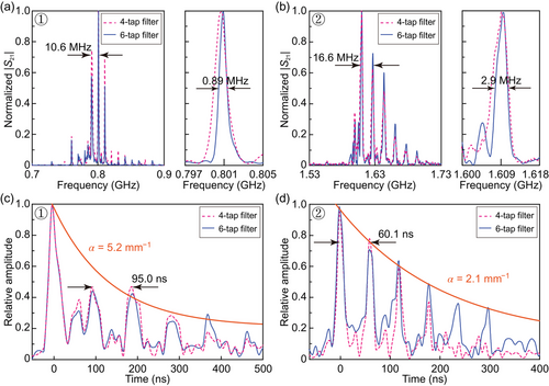
Next, we characterized the microwave filtering performance of our fabricated devices. The incident microwave drive power was set as −5 dBm for all measurements. Figure 5a,b shows the measured normalized |S21| spectra of 4- and 6-tap surface acoustic MWP filters with d = 2R = 268 µm at frequencies near 0.78 and 1.60 GHz. These spectra exhibit periodic passbands with an FSR of 10.6 and 16.6 MHz, corresponding to an acoustic delay of 94.3 and 60.2 ns, respectively, over the propagation distance d. Additionally, the passband bandwidth decreases as the number of the taps increases, achieving the smallest full width at half maximum of 0.89 and 2.9 MHz, respectively. Figure 5c,d plots the normalized impulse response, derived from the measured complex-valued frequency response in Figure 5a,b, respectively. Exponential fits of the decaying amplitude of the impulse response in Figure 5c,d indicate the propagation loss α of 5.2 and 2.1 mm−1 for the SAW modes ① and ②, respectively.

Since the FSR of the passbands depends on both the SAW velocity ʋ and the tap spacing d, we fabricated a series of 6-tap surface acoustic MWP filters with different tap spacings d, where R = d/2 satisfies the BIC condition for bent waveguides as shown in Figure 2a. We experimentally achieved time delays from 21 to 106 ns and measured the velocities of the two excited SAW modes as 2842 and 4904 m s−1 (see Section S2, Supporting Information). With these experimental results, we estimated the effective refractive index perturbation magnitude as Δneff = 4.7 × 10⁻⁶ RIU and the acousto-optic modulation depth as M = 4.75% (see Section S3, Supporting Information). These results can be further improved by optimizing the fabrication processes to reduce the optical loss and by optimizing the IDT structure to enhance the SAW excitation efficiency.
Compared with the Brillouin-based MWP filters,[42-44] where millimeter- or centimeter-long waveguide and milliwatt optical power are needed for producing sufficient stimulated Brillouin scattering (SBS) gain, our SAW-based MWP filters by utilizing the strong piezoelectric effect of lithium niobate can obtain a long delay time with a hundreds-of-micrometer-long acousto-optic modulation region and microwatt electrical power. Besides, since the SBS gain depends on the material's refractive index and elasticity, the Brillouin-based MWP filters are sensitive to fabrication processes and environmental temperature, thus having limited applications. Compared with the MWP filters on silicon-on-insulator platforms,[16, 17] which need hundreds-of-milliwatt optical power for stimulating SAWs and lack efficient tuning mechanisms, our SAW-based MWP filters can be tuned more easily by harnessing the excellent properties of lithium niobate. For example, the central frequency can be tuned by heating or cooling the device chip, and the delay time can be tuned by the electroacoustic and/or thermoacoustic effects.[20, 21] In addition, lithium niobate supports SAWs with a lower acoustic velocity (≈4000 m s−1) than that of silicon (≈5000 m s−1), and thus it is possible to obtain a longer delay time on the lithium niobate platform with the same device footprint.
Table 1 compares different types of MWP filters on integrated platforms. Here, the size refers to the effective length of optical waveguide. The link gain is defined as the ratio of the average RF output power to the average RF input power, which was obtained directly from the network analyzer. Among all the integrated MWP filters, ours feature a high resolution, compact device footprint, and low energy consumption. However, our MWP filters exhibit a relatively low link gain. This is attributed mainly to the low optical pump power on the chip, which was limited by the input laser power and the grating couplers' loss in our experiment. This optical pump power can be increased substantially by using edge-coupling scheme and low-noise optical amplifier. Additionally, further optimization of the IDT structure should lead to more efficient acousto-optic modulation, thus reducing the passband bandwidth and increasing the link gain even further.
| Platform | Type | Size | Center frequency [GHz] | Bandwidth [MHz] | Optical power [mW] | Link gain [dB] |
|---|---|---|---|---|---|---|
| GaInP[6] | Notch | 1.5 mm | 3–4 | 15 | 10 | −45 |
| InP[24] | Passband | 4.0 mm | 20 | 2500–5500 | NA | −20 |
| As2S3[8] | Passband | 11.7 cm | 3.6–30 | 140.0 | 40 | 22 |
| 20.8 | 80.0 | 15 | ||||
| Suspended silicon[10] | Passband | 5.0 cm | 3.9 | 6.2 | 105 | −17.3 |
| As2S3 on silicon[42] | Notch | 6.5 cm | 1.0–30 | 33–88 | 100 | NA |
| As2S3 on silicon[40] | Notch | 2.6 cm | 1–12 | 3 | 150 | −30–−10 |
| Silicon on insulator[17] | Passband | 2.4 mm | 2.4 | 5 | 10–300 | −104 |
| Silicon nitride[28] | Notch | NA | 5–20 | 400 | NA | 10 |
| Passband | NA | 5–20 | 400 | NA | 1.2 | |
| This work | Passband | 2.8 mm | 0.8 | 0.89 | 18 | −40 |
3 Conclusion
In conclusion, we have experimentally demonstrated surface acoustic MWP filters on an etchless lithium niobate integrated platform. The devices consist of a high-quality multitap photonic microcavity modulated by piezoelectrically excited surface acoustic waves. The devices operated under the principle of photonic bound states in the continuum for low-loss waveguiding and high-quality resonating and achieved high-performance in microwave filtering. We fabricated devices with 4 and 6 taps and realized an acoustic delay from 21 to 106 ns. Compared with other types of MWP filters based on Brillouin scattering and/or in a fiber-optic system, our surface acoustic MWP filters benefit from these competitive advantages: i) simple fabrication process which does not need etching of the substrate or suspension of delicate membranes or waveguides; ii) long time delay achieved within a small footprint due to the slow velocity of acoustic waves; iii) low energy consumption due to strong piezoelectric effect; iv) robustness against environmental perturbations such as vibrations and temperature gradients; v) easy extension of the microwave filtering concept to any other substrates and/or frequencies. With the superior properties of lithium niobate, the demonstrated surface acoustic MWP filters pave the way for a fully integrated MWP system on an LNOI chip, including light sources, amplifiers, modulators, signal processors, and photodetectors, with significantly enhanced compactness and system stability.
Acknowledgements
The authors would like to thank Mr. Piao Deng for his assistance with theoretical analysis. This work was supported by Research Grants Council of Hong Kong (No. 14206318, 14208421, C4050-21E) and The Chinese University of Hong Kong (Group Research Scheme).
Conflict of Interest
The authors declare no conflict of interest.
Open Research
Data Availability Statement
The data that support the findings of this study are available from the corresponding author upon reasonable request.


