Anisotropic polaritons in van der Waals materials
Funding information: Australian Research Council, Grant/Award Numbers: IH150100006, CE170100039; China Postdoctoral Science Foundation, Grant/Award Number: 2017M622758, LHTD20170006
Abstract
Polaritons in two-dimensional (2D) materials continues to garner significant attention due to their favorable ability of field-confinement and intriguing potential for low-loss and ultrafast optical and photonic devices. The recent experimental observation of in-plane anisotropic dispersion in natural van der Waals materials has revealed much richer physics as compared to isotropic plasmonic materials, which provides new insight to manipulate the polaritons and manufacture flat optical devices with unprecedented controls. Herein, we give an overview of the recent progress in in-plane anisotropic polaritons launched and visualized in the near-field range in 2D layered van der Waals materials. Furthermore, future prospects in this promising but emerging field are featured on the basis of its peculiar applications. This review article will stimulate the scientific community to explore other hyperbolic materials and structures in order to develop optical technologies with novel functionalities and further improve the understanding of the exotic photonic phenomena.
1 INTRODUCTION
Polaritons—collective excitations formed by the coupling of photons with oscillating charges—in van der Waals materials provide a new way to manipulate light at nanoscale. Until now, various types of polaritons in van der Waals crystals, including those formed by free electrons (plasmon polaritons),1-5 strongly-bound electron-hole pairs (exciton-polaritons),6-8 and bound lattice vibrations (phonon polaritons [PhPs])9-11 have been discovered and already shown promising potentials in light-based technologies beyond diffraction limit spanning a broad range of the electromagnetic spectrum.12, 13 Among these polaritons, PhPs with hyperbolicity attracted significant attention due to their strong field confinement, low losses, and long lifetimes.14 Basically, the nature of light propagating inside a medium can be described by the dielectric permittivity tensor ( ε = diag [ε x, ε y, ε z]) at such frequency, where ε x, ε y are the in-plane components and ε z is the out-of-plane component. 15 Many distinctive and non-intuitive optical phenomena associated with polaritons require negative perimittivity.16, 17 The peculiar properties of light propagation in a medium stem from the isofrequency surface in the momentum space, which are defined by the sign of ε i(i = x, y, z) . When the medium is crystallographically anisotropic, it will hold different dielectric responses along different directions. If one of the permittivities, that is, ε i(i = x, y, z), is opposite in sign to the other two components, such medium then exhibits hyperbolicities,18, 19 which are the key to a range of sub-diffractional optical phenomena, such as negative refraction,20, 21 hyperlens,22-24 nanolithography,25, 26 and enhancement of quantum radiation.27 Furthermore, when ε x * ε y < 0,the hyperbolicities can also exist in the planar surface.28, 29
Theoretically, the polaritons propagate along the layers with an in-plane anisotropic dispersion in case of different permittivities along orthogonal in-plane directions. The polaritons show an elliptic in-plane dispersion, subject to different permittivities but with the same signs whereas; for different signs, the polaritons possess an in-plane hyperbolic dispersion. The prominent example of hyperbolic natural material is hexagonal boron nitride (hBN).9, 14 The hBN is a polar van der Waal material with uniaxial permittivities possessing two mid-infrared Reststrahlen bands, one of which spans from 1395 to 1630 cm−1 (for the case of enriched hBN), where ε x = ε y = ε⊥ < 0 (the in-plane permittivity is negative and isotropic) and ε z = ε∥ > 0 (the out of plane permittivity is positive).23, 24, 30 Therefore, the PhPs in hBN show an out-of-plane hyperbolic dispersion and isotropic in-plane dispersion.23, 24, 28, 31, 32 Although the PhPs with in-plane hyperbolic dispersion can be induced in nanostructured hBN (ie, artificial metamaterial), its visualization in natural materials was highly desirable.33 Recent discovery of anisotropic polariton propagation along the surface of a natural vdW α-MoO3 flakes demonstrates PhPs with elliptic and hyperbolic in-plane dispersion,34, 35 promise substantial advances in the fields of infrared optics and nanophotonics.36 Contrary to artificial metamaterials with delicate designs, anisotropic polaritons in natural vdW materials with in-plane hyperbolic dispersions could manipulate light with unprecedented controls especially with subdiffractional confinement, low losses, and polarization sensitivities.4, 34
In this review, we summarize the recent progress of planar anisotropic polaritons on their near-field responses with an emphasis on the natural layered materials, which may exhibit more potentials than conventional metasurfaces at some frequency ranges with critical applications. Firstly, we introduce the real-space nanoimaging mechanism by using scattering-type scanning near-field optical microscopy (s-SNOM) and summarize the research progress of polaritons in 2D materials. The basics of anisotropic polaritons with hyperbolic/elliptic dispersions are then discussed. After briefly reviewing the hyperbolic metasurfaces, we focus on the natural layered system for in-plane anisotropy and present several potential applications taking advantage of its unique abilities to control light. This review is aimed at providing a timely overview of the potential development of naturally hyperbolic media in novel optical devices. It is extremely attractive that naturally in-plane anisotropic materials may thus establish a new paradigm in nanophotonics, promising an unprecedented potential for the directional control of light and light-matter interactions at the nanoscale.
2 DIRECT VISUALIZATION OF POLARITONS IN REAL SPACE
Polaritonics provides a unique way to harness, guide, and manipulate light at nanoscale much smaller than the diffraction limit.37 Initially, surface plasmon polaritons in metals set an early stage for investigating this distinctive branch of optics.38-40 However, the loss associated with electron/plasma scattering and interband transitions is unacceptably large.41, 42 The emergence of 2D materials offers new opportunities to explore low-loss polaritons compared with metal plasmonics. The development of the real-space nanoimaging technique has allowed us to directly observe these highly confined polaritons in the near field and conveniently study the fundamental physics of low-dimensional materials.12, 13 Featuring a wavelength-independent nanoscale spatial resolution (~10 nm, determined by the diameter of the tip apex), s-SNOM provides deterministic observations and characterizations of various polaritons in real space.43 As an important visualization technique, it shows an exceptional capability of unfolding quantum phenomena.1, 9, 33, 34, 44, 45 Specifically, infrared (IR) light is focused onto a high-frequency oscillating metallic tip of an atomic force microscope. The tip functions as an optical antenna that effectively generates optical near-fields with wave vectors much larger than that of the incident light, which thus can match the excitation conditions of the polaritons in the materials of interest. Generally, the propagating properties and the wavelength of a polariton can be extracted from the local optical field and periodicity of the interference fringes in s-SNOM images.1, 2 The dispersion relation of the polariton is thus attainable, along with the quantitative measure of the propagation loss from the real-space imaging. A detailed review of the development of the s-SNOM technique can be found in a reference by Chen et al.43 Hyperspectral imaging by the nanoscale Fourier transform infrared (nano-FTIR) spectroscopy can also offer the nanometer spectral and spatial resolution to study polaritonic behaviors as the tip is raster-scanned over the sample (line-scans), which is often employed as a powerful tool complimentary to monocharmatic single-frequency imaging by the s-SNOM.46-48
By utilizing s-SNOM, Chen et al1 and Fei et al2 (independently) demonstrated the real-space imaging of the polaritonic waves in graphene, in 2011, for the first time. Particularly, the strong light confinement, gate-tunability, and long lifetimes can be found in such an atomically thin layer (Figure 1A). Graphene plasmonics not only opens an avenue for applying plasmon polaritons in graphene into low-loss gate-tunable nanophotonic devices, but also inspires the discovery of potential polaritons in other 2D materials. PhPs in hBN, distinctive from plasmons in graphene, were observed by Dai and coworkers in 2014,9 whereas these lattice-vibration-dependent PhPs can be sustained in hBN down to few layers (even monolayer in their recent study50). (Figure 1B). Polaritons with highly low losses can exist in hBN as volume-confined modes that stem from the large birefringence between in-plane and out-of-plane. Details will be discussed in the following parts. Different from the spectral investigation of strongly coupled cavity exciton-polaritons, Fei7 and Hu et al6 observed the real-space propagation of exciton-polariton waveguide modes in layered WSe2 and MoSe2 at room temperature (Figure 1C). The nano-optical imaging of exciton-polaritons clearly unveils the high sensitivity of the polariton propagation length to the excitation energy, with a large propagation length up to 12 μm allowing for long-range energy or information transfer in future nanophotonic circuits.
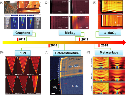
To overcome the limitations of the individual polaritons, atomic-scale photonic hybrids of van der Waals heterostructures provide an extra degree of freedom to tune these polaritons (Figure 1D).49, 51 For example, the graphene/hBN heterostructure supports a new form of hybrid plasmon-PhPs with a broad bandwidth range and long lifetime that can be actively controlled through electrical gates.52-56 Recent observations of the anomalous propagation of polaritons on infrared hyperbolic surfaces uncovers the novel physics in these layered materials (Figure 1E,F).33, 34 The in-plane hyperbolic polaritons in both natural α-MoO3 and nanostructured hBN metasurface show the great potential of squeezing infrared light with directional control and ultralow loss. Moire polaritons based on twisted 2D bilayers have also attracted significant interest recently, including the directed propagation control of surface plasmons in Moire graphene superlattice,57 Moire excitons in twisted stacks of monolayer transition metal dicalcogenides58 and phonon based soliton superlattices in twisted hBN.59 Therefore, the study of polaritons in 2D materials is a vibrant area of research at the vanguard of materials science, engineering, physics, and biology, where anisotropic polaritons play a fascinating role in manipulating the nano-light with orientational selectivity (Table 1).
| Material | Polariton types | Tunability methods | Lifetime | Refs. |
|---|---|---|---|---|
| Graphene |
|
|
Near 2 Ps | 1-3, 54, 60 |
| BP |
|
|
NG | 5 |
| hBN |
|
|
Near 8 Ps | 9, 14, 61-64 |
| α-MoO3 |
|
|
Over 8 Ps | 34, 35, 65 |
| WSe2 |
|
|
NG | 7, 66 |
| MoSe2 |
|
|
NG | 6 |
| MoS2 |
|
|
NG | 67 |
- Note: Not including heterostructures here.
- Abbreviations: BP, black phosphorus; hBN, hexagonal boron nitride; NG, not given.
3 BASICS OF ANISOTROPIC POLARITONS
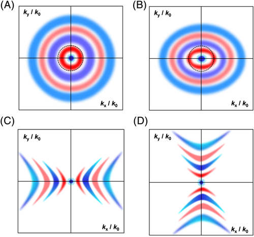
As referred above, the nature of light propagating inside a medium can be described by the iso-frequency contour in the k-space. Briefly, the momentum k corresponding to each wavelength of polaritons can be defined by permittivities at constant ω. The dielectric permittivity is a frequency-dependent tensor ( ε = diag [ε x, ε y, ε z], where ε x, ε y are the in-plane components and ε z is the out-of-plane component. If the permittivity tensors (along different axes) are of opposite signs, the medium is called hyperbolic materials.9, 10, 15, 18, 19 The strong optical anisotropy will render a series of potential applications in nanophotonics including negative refraction, hyperlens, and enhanced quantum radiation.68-73 Normally, hyperbolic media was often discussed in the context of metamaterials, which aim at the novel properties that are not attainable in a natural system by “meta-atom.” The detailed review of this aspect can be referred to the reference by Alexander et al.19 Recently, the bulk hyperbolicity was observed in the natural system—hBN, which has emerged as a new platform for investigating sub-diffractional imaging and focusing, ultraslow hyperbolic polariton propagation, negative group velocity, and the hybridization of two different classes of propagating polaritons.11 Actually, many bulk hyperbolic materials has been identified in nature, such as graphite,74 magnesium diboride,75 quartz,76 tetradymites,77 calcite,78 and α-Al2O3 single crystal.79 However, both the hyperbolic metamaterials and naturally hyperbolic materials can be defined by the different signs of permittivity between in- and out-of-plane. Generally the polaritons supported by these mediums are in-plane isotropic, it is challenging to realize optical functionalities for particular orientations and polarization in the planar surface, which are essential for high-performance polaritonic applications such as imaging and energy transfer devices.80, 81

4 HYPERBOLIC METASURFACES
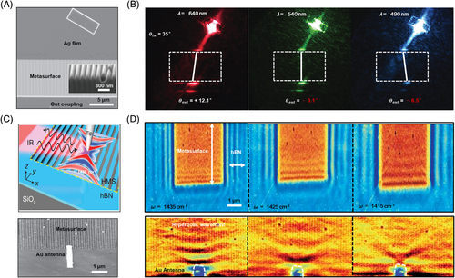
One effective way to achieve extremely large wave confinement and local density of states is to artificially reconstruct thin layers of an isotropic materials. Such manmade media can support the in-plane hyperbolic polaritons with ultra-high momentum. Through the manmade metallic gratings, one can drastically modified the dispersion of surface plasmons.88 The periodic metallic gratings could support the propagation of surface polaritons with hyperbolic wavefront and orientational selectivity. The theoretical predictions have been readily verified in later experiments based on the hyperbolic metasurface of artificial silver/air gratings at visible frequency (see Figure 3A,B).89 The device indicated clear planar negative refraction and diffraction-free propagation. The hyperbolic metasurface was also verified by anisotropic metallic arrays at microwave frequencies.90 Gomez-Diaz et al showed the possible realizations of hyperbolic metasurface at terahertz using nanostructured graphene.91 Very recently, Li et al demonstrated the infrared hyperbolic metasurface by nanostructuring hBN that supports highly confined anisotropic PhPs (see Figure 3C,D).33 Compared with metallic surface plasmon polariton, the PhPs in hBN have notably low loss. By appropriately engineering the “meta-atoms,” one may obtain different hyperbolic metasurfaces at some frequency ranges.92 However, the noteworthy losses associated with plasmonic materials used in artificial hyperbolic surface and undesirable confinement at long wavelength range (kp ≈ k0) could result in the unsatisfactory performance of optical devices. Moreover, the losses induced by fabrication imperfections are inevitable. The maximum momentum of propagating polaritons is determined by the inverse size of “meta-atom,” the optical device will be cutoff when approaching this ultimate momentum. Although the hyperbolic mediums are also called indefinite materials because of the open curve of iso-frequency contour (ideally indefinite k), the metamaterials do not hold the key to the full potential of hyperbolic medium. Recently, it was demonstrated that some natural materials could offer advances in the realization of in-plane hyperbolic surface.34, 35 In particular, the natural α-phase molybdenum trioxide (α-MoO3) and black phosphorus (BP), which have strong in-plane optical anisotropy, hold great promise for directional control of the polariton—propagation.
5 NATURALLY IN-PLANE ANISOTROPIC POLARITONS
Since the discovery of graphene, research on various 2D materials has boomed in the fields of material science, chemistry, physics, biology, and nanotechnology.93, 94 Among the broad array of 2D materials, some in-plane anisotropic materials play important roles in optical and electronic applications.12, 13, 68, 95 The most striking feature of such 2D materials is the naturally high in-plane anisotropy of its macroscopic physical properties, which arises due to its special orthorhombic lattice. Here, we will review the progress on naturally anisotropic materials with a particular emphasis on α-MoO3 and BP, and mainly focus on their advance in terms of in-plane anisotropic polaritons. As discussed above, the directional propagation of polaritons in the plane results from large in-pane optical anisotropy. The in-plane anisotropic media often support anisotropic polaritons (like Dyakonov surface wave).96, 97 Large optical anisotropy is generally found in structurally anisotropic materials, for example, strong birefringence or dichroism has been observed in biaxial crystals with orthorhombic structure. Among those materials, both α-MoO3 and BP have interesting orthorhombic-layered structure.
The schematics of Figure 4A shows the crystal structure of α-MoO3, where layers formed by distorted edge-shared MoO6 octahedra are weakly bonded by van der Waals forces. The α-MoO3 lattice constants a, b, and c, along the three directions in space (x, y, z) are all different. In each double layer structure, MoO6 forms corner-sharing chains along the [001] direction and edge-sharing chains along the [100] direction (shown in Figure 4A). Three O atoms differently linked with one Mo atom, of which O2-Mo is along the [001] direction and O3-Mo along the [100] direction. The α-MoO3 has a strong in-plane structure anisotropy as the difference of the spacing between (100) facets and (001) facets is as large as 7.2% Consequently, α-MoO3 is a biaxial material with strong in-plane anisotropy. Similar to α-MoO3, BP atomic layers are stacked together with van der Waals force while the single layer is bonded by sp3 phosphorus atoms, as shown in Figure 4B. The BP layer-to-layer spacing is around 0.52 nm. As shown in side-view from different in-plane perspective, BP displays a strong in-plane anisotropy between the crystal orientations along “zigzag” and “armchair” directions.
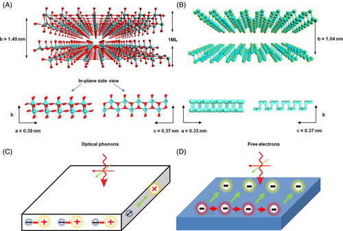
The crystal structure of these two materials has conspicuous differences along two orthogonal directions in the plane. Consequently, the dielectric function is highly in-plane anisotropic resulting from variations in the real part of permittivity as a function of in-plane directions. It is noteworthy the strong in-plane anisotropy of permittivity at resonance frequencies can render directional propagation of polaritons. This indicates that natural α-MoO3 and BP crystals can be the good candidates that support in-plane anisotropic polaritons so as to realize the natural hyperbolic surface. Besides, many theory works predicted the polaritons with in-plane directional propagation behavior in natural materials.29, 91, 98-103 All of these in-plane anisotropic polaritons can be inherited by the different collective oscillations of electrons or optical phonons along different directions. The low in-plane lattice symmetry leads to distinct anisotropy.
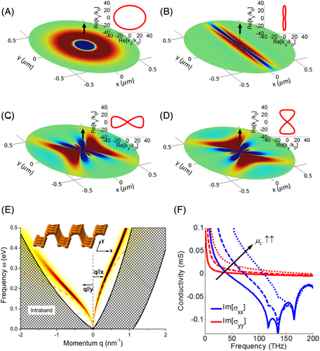
One should note that the mechanisms of in-plane optical anisotropy in BP and α-MoO3 are essentially different. In case of BP, the 2D description of anisotropic polaritons was based on its anisotropic conductivity.4, 99 The interplay between interband and intraband motions renders different oscillations of electrons—in-plane anisotropic plasmon polaritons, as illustrated in Figure 4D. Generally, if an antenna (metallic nanostructure) is used to launch the polaritons in polaritonic materials, the polaritons propagate away from the antenna as circular waves in many cases such as those in graphene, hBN, SiC, and so on. In BP, the inductive optical response along two in-plane axes enables the hyperbolic rays launched by an antenna.29 If a z-oriented dipole emitter is used to launch the polaritons along homogeneous surface (as shown in Figure 5A-D), one can observe different polaritonic isofrequency contours while tuning the anisotropic conductivity. The hyperbolic plasmons and topological transitions can also be expected over the planar surface. In the highly anisotropic regime (Im σx * σy < 0), the plasmon propagating along some direction are totally forbidden (shown in Figure 5E,F).4, 102 The dispersion relation imply that the resonance modes can be found only along x axis in some frequency regime (ie, above 0.47 eV), as presented in Figure 5E. The principal components of the conductivities in BP have opposite signs (Figure 5F, ie, σ xxσ yy < 0), which are the signatures for in-plane hyperbolic plasmon. There are a few ways to modulate the imaginary parts of BP conductivity, such as optical and chemical doping, so as to tune the in-plane anisotropy.103-105 Although BP is a great candidate to investigate directional control of the propagation of plasmon polaritons,100, 106 the experimental observation of in-plane anisotropic polaritons propagating in BP has still remained elusive so far, due to the lack of suitable lasers as excitation mid/far-IR light coupled into s-SNOM. Recently, the theoretical studies on electromagnetic modes in biaxial slabs and accurate infrared anisotropic permittivities of α-MoO3 were further developed.107, 108
Another mechanism of optical in-plane anisotropy relies on highly discrete optical phonons. For polar crystal (eg, SiC and α-MoO3), the anisotropic optical-phonons often result in multiple spectral ranges that are assigned to “Reststrahlen bands” (RBs),109 resulting from a long-wavelength incident optical field in the resonance frequency range. The strength of resonances always shows a strong dependence on the polarization of the excitation beam, as illustrated in Figure 4C. For example, α-MoO3, a polar van der Waals crystal, has received considerable attention over the past decade for nanoscale light-control because of strong birefringence in this material. Ma et al experimentally observed the low-loss hyperbolic and elliptical polaritons in natural α-MoO3 crystals. In this work, novel in-plane hyperbola-type anisotropy in the form of hyperbolic PhPs, resulting from in-plane anisotropic dispersion, was reported. Utilizing high-resolution s-SNOM technique, the polariton interferometry images show strong direction-dependence, as revealed in Figure 6A-D.34 Interestingly, the interference pattern in the upper-RB (U-RB) depicts an elliptical shape with the largest PhPs wavelength along the [001] surface direction, whereas it transforms into an almond shape in the lower-RB (L-RB) with the largest wavelength along the [100] direction. The Fourier transform analysis of Figure 6A,B gives an ellipsoid in the U-RB (Figure 6C) and hyperbola in the L-RB (Figure 6D), revealing that the PhPs exhibit elliptic and hyperbolic dispersions, respectively. More strikingly, the anisotropic polaritons in α-MoO3 have ultra-long amplitude lifetimes (up to 20 pico-seconds), offering new opportunities for sub-wavelength planar device aiming at directional modulation of ultra-fast light-matter interactions (usually at femto-seconds or pico-seconds range).
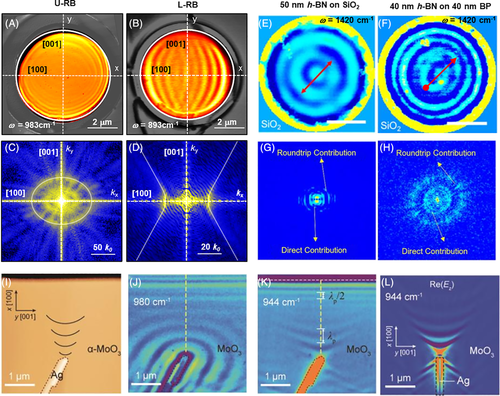
Unlike the polaritons in graphene and hBN, the wavefront of the in-plane hyperbolic polaritons exhibit the particular shape in sharp contrast to concentric rings. The anomalous (concave) wavefronts can be launched by a silver antenna on top of the α-MoO3 sheet (Figure 6I-L).35 The exotic wavefronts further indicate strong optical anisotropy in α-MoO3. The giant optical in-plane anisotropy in natural barium titanium sulfide (BaTiS3) was also reported by Niu et al.111 However, the in-plane anisotropic polaritons were not referred to in this work. The in-plane hyperbolic polaritons in van der Waals materials own the unusual features of hyperbolicity in bulk hyperbolic metamaterials, making it intriguing for exotic optical applications such as negative refraction,20, 21 hyperlens,22-24 and enhancement of quantum radiation.27 Most importantly, all these phenomena are realized in a planar surface rather than complicated structures, rendering easier accessibility.
Although the anisotropic plasmon polaritons have not been experimentally observed in intrinsic BP, the anisotropic dispersion in BP can be utilized to modulate the in-plane polaritons in hBN by constructing a vertical heterostructure of BP and hBN. The PhPs in hBN have prompted intensive investigations on the low-loss and volume-bound nature of hyperbolic PhP modes. Nevertheless, the intrinsic PhPs in hBN normally propagate as a cylindrical wave in hBN sheet, manifesting as in-plane isotropic nature. However, the propagation behavior of polaritons in hBN will be modified while a piece of hBN disk is placed on top of a piece of BP nanosheet. In particular, anisotropic polaritonic modes can be observed along zigzag and armchair axes of BP, as shown in Figure 6E-H.110 More specifically, the nanoimaging results show characteristic elliptical interferometry pattern in hBN/BP heterostructure (Figure 6F) in contrast with an concentric pattern in pure hBN (Figure 6E). This could be a general approach to achieve tailored anisotropic optical properties by stacking two van der Waals materials with different optical birefringencies to form a new metasurface. From point of view of polaritonic regime, longitudinal optical phonon-plasmon coupling effect could also be another way to modulate the anisotropic properties of polar semiconductor.105, 112
6 CONCLUSIONS AND OUTLOOK
In this review, we briefly reviewed the recent progress of the 2D polaritonic materials. Particular attention is paid to natural van der Waals materials that have in-plane optical anisotropy in terms of anisotropic dispersion, which enables anisotropic phonon or plasmon polaritons. Inspired by the mechanisms for optical in-plane anisotropy, that is, the interplay between anisotropic electron motions can support anisotropic surface plasmon, this concept could also be generalized for other materials with similar structure as BP, for example, semimetals like MoTe2, WTe2.113, 114 On the other hand, similar to α-MoO3, anisotropic crystals such as V2O5115 and WO3116 are also potential candidates to support anisotropic propagation of polaritons. It is worth mentioning here that external parameters like pressure and doping can tune the materials properties as well and therefore their implements in polaritonics or plasmonics will further enrich our basic understanding of underlying physical phenomenas, which can stimulate more fundamental or technological breakthroughs for practical nanophotonic applications.
Compared with traditional metasurface, naturally anisotropic materials are not limited to the size of “meta-atom” which is corresponding to the maximum momentum of polaritons that can be supported. Such natural hyperbolicity could induce an extremely small wavelength, resulting in miniaturized optical devices for sensing, signal processing and quantum computing. Also, the use of natural materials can avoid time-consuming fabrication and eliminate the high inherent losses associated to fabrication processes. There is a great deal of polaritonics based on natural 2D materials, which are particularly suitable for the planar and directional light modulation with on-chip integration. Although the polaritonics of naturally in-plane hyperbolic materials is still an emerging research field, one can envision many distinctive phenomena such as planar negative refraction, waveguiding, hyperlensing, waveplate, and engineering of exotic wavefront of polaritons for the near future. Finally, the natural in-plane hyperbolic materials could open new possibilities for energy control and assist directional heat transfer with extreme efficiency.
ACKNOWLEDGMENTS
B.S. acknowledges the funding support from the China Postdoctoral Science Foundation Grant (No. 2017 M622758). Q. Bao acknowledges the support from the Australian Research Council (ARC, IH150100006, FT150100450, and CE170100039).
CONFLICT OF INTEREST
All the authors declare that they have no conflict of interest.
Biographies

Weiliang Ma is currently a research assistant in Optoelectronics and School of Optical and Electronic Information, Huazhong University of Science and Technology, China. He received his BSc and MSc both in physics from Soochow University, Suzhou, China in 2015 and 2018. His main research interests are 2D materials and nanophotonics.

Babar Shabbir is currently a research fellow at Department of Material Science and Engineering, Monash University. In 2016, Babar graduated from University of Wollongong, Australia with a PhD in physics. Before that, he graduated with MSc (2006) and MPhil (2009) in physics from Quaid I Azam University, Pakistan. His research area is two-dimensional materials with a particular focus on light matter interaction applications.

Qiaoliang Bao received his BA (2000) and ME (2003) degrees in Materials Science and Engineering from Wuhan University of Technology (China). He obtained his PhD degree (2007) in Materials Physics and Chemistry from Wuhan University (China). He worked as postdoctoral fellow at Nanyang Technological University and National University of Singapore from 2007 to 2012. He was appointed as a tenured associate professor at Department of Materials Science and Engineering, Monash University in 2016. His research interests include waveguide-coupled 2D semiconductors and polariton-coupled 2D materials and devices, focusing on the effect of confined-space light-matter interactions on the transport of electrons or other quasi-particles such as plasmon polariton, exciton polarition, and phonon polariton.


