A universal reverse-cool annealing strategy makes two-dimensional Ruddlesden-popper perovskite solar cells stable and highly efficient with Voc exceeding 1.2 V
Zhongqi Xie and Huiming Luo contributed equally to this study.
Abstract
Two-dimensional Ruddlesden-Popper (2D RP) layered metal-halide perovskites have garnered increasing attention due to their favorable optoelectronic properties and enhanced stability in comparison to their three-dimensional counterparts. Nevertheless, precise control over the crystal orientation of 2D RP perovskite films remains challenging, primarily due to the intricacies associated with the solvent evaporation process. In this study, we introduce a novel approach known as reverse-cool annealing (RCA) for the fabrication of 2D RP perovskite films. This method involves a sequential annealing process at high and low temperatures for wet perovskite films. The resulting RCA-based perovskite films show the smallest root-mean-square value of 23.1 nm, indicating a minimal surface roughness and a notably compact and smooth surface morphology. The low defect density in these 2D RP perovskite films with exceptional crystallinity suppresses non-radiative recombination, leading to a minimal non-radiative open-circuit voltage loss of 149 mV. Moreover, the average charge lifetime in these films is extended to 56.3 ns, thanks to their preferential growth along the out-of-plane direction. Consequently, the leading 2D RP perovskite solar cell achieves an impressive power conversion efficiency of 17.8% and an open-circuit voltage of 1.21 V. Additionally, the stability of the 2D RP perovskite solar cell, even without encapsulation, exhibits substantial improvement, retaining 97.4% of its initial efficiency after 1000 hours under a nitrogen environment. The RCA strategy presents a promising avenue for advancing the commercial prospects of 2D RP perovskite solar cells.
1 INTRODUCTION
Perovskite solar cells (PSCs) have received much attention because of their high absorption coefficient, large charge carrier mobility, and excellent photovoltaic performance.1, 2 At present, through diligent optimization of fabrication protocols, the maximal power conversion efficiency (PCE) of PSCs has experienced a precipitous increase, attaining values exceeding 26%.3, 4 Except for the PCE, operational stability is another key parameter that needs consideration toward commercialization.5-7 It is interestingly found that two-dimensional Ruddlesden-Popper (2D RP) PSCs display long-term environmental stability by introducing bulky large cations (e.g., phenylethylammonium (PEA), 4-fluorophenylethylammonium (4FPEA)).8, 9 However, carrier transport ability is suppressed due to the quantum confinement effect and random crystal orientation of 2D RP perovskite films.10 Thus, the photovoltaic performance of 2D RP PSCs is still lower than that of their 3D counterparts.11
Various strategies are proposed to fabricate highly efficient and stable 2D PSCs, including solvent engineering, additive engineering, and cation engineering.12-16 Zhu and co-workers adjusted the content of dimethyl sulfoxide (DMSO) in precursors to tune the quality of obtained 2D RP perovskite (PEA)2(MA)4Pb5I16.12 Additives like Lewis acids and Lewis bases were employed to assist the crystallization of 2D RP perovskite films and induce the out-of-plane direction.17, 18 For example, ammonium thiocyanate (NH4SCN) was employed as an additive to control crystallographic orientation of 2D RP perovskite films, leading to high-efficiency charge transport.18 Besides, the bulky large cations were also explored to improve the PCE of 2D RP PSCs by tuning their crystal structure.19 Shao and colleagues have illustrated this concept by substituting phenylethylammonium (PEA) with 4-fluorophenethylammonium (4FPEA), resulting in an impressive increase in PCE of 2D RP PSCs, from 11.1% to 17.3%.8 The enhancement of PCE is attributed to the fast charge dissociation and preferentially grown along the out-of-plane direction by inducing the fluorinated PEA cation. Meanwhile, the environmental stability of PSCs is also improved owing to the hydrophobic property of fluorinated cation.8 Although those strategies can improve PCE and stability of 2D RP PSCs, the complexity and uncontrollability of 2D RP perovskite films still need further exploration.
The quality of 2D RP perovskite films is in correlation with the photovoltaic performance of PSCs. As the evaporation rate of solvents, nucleation and growth rate of grains are highly dependent on annealing processes of 2D RP perovskite films. Therefore, the annealing strategy is very important process to promote the ordered distribution of multiple phases along the out-of-plane direction. For example, a hot-casting strategy was used to fabricate the uniform 2D RP perovskite films with excellent crystallinity, providing the more charge-transport channels.20, 21 2D RP perovskite (4FPEA)2(FA0.3MA0.7)4Pb5I16 (n = 5) was fabricated by a hot-casting strategy (e.g., the substrate heated to 100 °C) and exhibited a preferential vertical orientation.11 However, the repeatability of 2D RP PSCs obtained from a hot-casting strategy needs to be further optimized, due to the quality of 2D RP perovskite films being deeply reliant on substrate temperature.22 Additionally, several annealing strategies, such as close-space annealing and two-second-annealed methods, are still explored for the fabrication of perovskite films in detail.23, 24 Interestingly, a nonisothemal strategy was also used to fabricate high-quality perovskite films through illuminating wet film by a NIR lamp with temperature more than 100 °C.25 The perovskite films with high phase stability, small surface lattice space, and high bonding energy were also fabricated by an air-processed thermal-shocking strategy with high temperature above 180 °C.26 From the above discussion, the flash crystallization process with high nucleation and growth rate has been obtained by the flash-annealing approach, which is beneficial to fabricating high-quality perovskite films. Therefore, it is highly desirable to develop a novel flash-annealing approach to fabricate 2D RP PSCs.
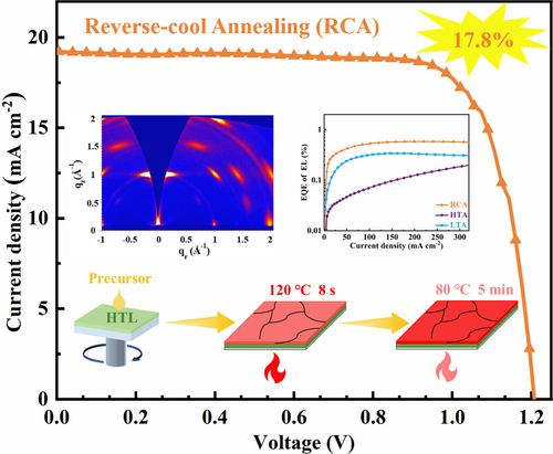
In this work, 2D RP perovskite (4FPEA)2(MA0.9FA0.1)3Pb4I13 films are fabricated by reverse-cool annealing (RCA) strategy. The first step accelerated the nucleation and growth of 2D RP perovskite films by annealing at 120 °C for 8 s. The second step is strengthening the crystal quality by annealing at 80 °C for 5 min. Additionally, 2D RP PSCs preferentially grow along the vertical direction. The results demonstrate that 2D RP perovskite films display high crystallinity, long charge lifetime, and strong carrier transport ability. As a result, the 2D RP PSC with RCA shows a significant PCE of 17.8%, which is higher than those of the 2D RP PSCs with high-temperature annealing (HTA) (7.8%) and low-temperature annealing (LTA) (12.7%).
2 RESULTS AND DISCUSSION
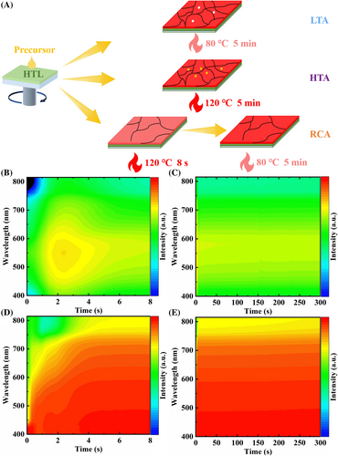
Two-dimensional Ruddlesden-Popper perovskite (4FPEA)2(MA0.9FA0.1)3Pb4I13 films are fabricated by three different annealing strategies, including LTA, HTA, and RCA. Figure 1A shows the fabrication process of perovskite films based on LTA, HTA, and RCA. In the LTA strategy, the wet perovskite films are heated at 80 °C for 5 min, resulting in as-prepared perovskite films with some pinholes. The in situ absorption evolution during the annealing process for the perovskite film based on LTA are shown in Figure 1B,C. The absorption spectrum red-shifts after placing the wet perovskite film on a hot platform at 80 °C. However, the weak absorption intensity of the absorption spectrum indicates the formation of perovskite crystallites.21 For the HTA strategy, a temperature as high as 120 °C is used to obtain perovskite films. It is observed that high annealing temperature (e.g., 120 °C) damage the crystal quality of the obtained perovskite films by exposing PbI2 crystal grains. From Figure 1D,E, the crystallization reaction is triggered by the high temperature of 120 °C in 1 s after placing the wet perovskite film on a hot platform. After approximately 6–8 s, the absorption spectrum of the perovskite films rapidly red-shifts, signifying the formation of the perovskite film. And then the absorption spectrum eventually exhibits a continuous profile. Therefore, the optimized time of high temperature annealing process is around 8 s. Regarding the effects of annealing time for both LTA and HTA, the photovoltaic parameters are displayed in Table S1. The RCA strategy, on the other hand, effectively improves the crystal quality of the perovskite films. In this approach, the wet perovskite films are heated at 120 °C for 8 s to achieve a high nucleation and growth rate during the first step, which promotes crystal growth along the out-of-plane direction, as shown in Figure S1a. Subsequently, the low-temperature annealing step (80 °C for 5 min) in the second stage further facilitates the formation of the uniform and smooth perovskite films. To clarify the effect of the low-temperature annealing step, the perovskite film with annealing at 120 °C for 8 s (marked as HTA-8) is characterized by the steady-state photoluminescence (PL) spectra, as shown in Figure S1b. The PL intensity of perovskite film with RCA is larger than that of the perovskite film with HTA-8, demonstrating the improvement the perovskite crystallization quality through low-temperature annealing step. Furthermore, the corresponding perovskite films are used to fabricate PSCs. Figure S2 shows J-V curves of the PSCs based on RCA and HTA-8. The photovoltaic performance of the PSC with RCA is higher than that of the PSC with HTA-8 with the detailed data in Table S2.
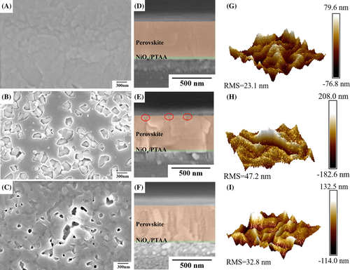
To verify the aforementioned hypothesis, the morphologies of perovskite films were characterized by scanning electron microscope (SEM) and atom force microscope (AFM). Figure 2A–C shows plane-view SEM images of perovskite films produced through LTA, HTA, and RCA. From Figure 2A and Figure S3, the RCA-based perovskite film exhibits a notably compact and smooth surface. As can be seen in Figure 2B, a deleterious impact on the surface of the HTA-derived perovskite film is apparent. The white regions denote the presence of PbI2 crystal grains, resulting from the decomposition of perovskite films.27 In contrast, as depicted in Figure 2C, it is evident that the LTA-derived perovskite film displays conspicuous pinholes and grain boundaries. Figure 2D shows the cross-sectional SEM image of the RCA-derived perovskite film. Interestingly, continuous large grains with almost no grain boundary are obviously observed for the RCA-derived perovskite film. The thickness of the RCA-derived perovskite film is approximately 440 nm. The strong smooth surface and vertical-orientation of the RCA-derived perovskite film is beneficial for improving the charge transport and extraction ability, resulting in the dramatic improvement of short-circuit current density (Jsc). From Figure 2E, it is also found that the HTA-derived perovskite film is destroyed. The LTA-derived perovskite film shows few random-oriented small crystalline grains, as shown in Figure 2F. In RCA strategy, the high temperature step is beneficial to obtain the continuous large grains and the low-temperature annealing step further promotes the formation of the high-quality perovskite films. In addition, the thickness of the HTA- and LTA-derived perovskite films is similar to that of the RCA-derived perovskite film. AFM images were applied to analyze the roughness of perovskite films. From Figure 2G–I, the root-mean-square (RMS) values of perovskite films based on RCA, HTA, and LTA are 23.1, 47.2, and 32.8 nm, respectively. The results indicate that the RCA strategy effectively promotes the formation of ideal perovskite films.
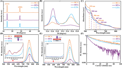
The crystallinity of perovskite films is confirmed by X-ray diffraction (XRD) measurement, as shown in Figure 3A. The diffraction peak at 14.2 ° of (111) plane for the RCA-based perovskite film has a higher intensity than those of the HTA- and LTA-based perovskite films.11 The diffraction peaks at around 28 ° are observed for all perovskite films, which can be assigned to the (202) plane.11 Furthermore, the peaks at around 28 ° can be split, due to the (004) plane of 3D-like perovskite phase.28 Especially, the HTA-based perovskite film shows the visible diffraction peak of PbI2 at 12.6 °, as shown in Figure 3B.29 The exposed PbI2 comes from the dissociation of perovskite films, which is consistent with the SEM image (Figure 2B). The results indicate that the RCA strategy promotes crystal growth of perovskite films. Meanwhile, RCA- and LTA-based perovskite films show a diffraction peak at 15.5 °, which can be assigned as the (100) planes of MAPbCl3 crystals.30 The related reports demonstrate that MAPbCl3 clusters are formed from MACl and PbCl2, which is beneficial for obtaining a compact and pinhole-free perovskite film.31
| Film | d (nm) | τPVK (ns) | τPCBM (ns) | τHTL (ns) | LD,e (nm) | LD,h (nm) |
|---|---|---|---|---|---|---|
| RCA | 440 | 56.3 | 33.4 | 21.4 | 232.1 | 357.9 |
| HTA | 440 | 10.1 | 9.0 | 8.1 | 98.0 | 139.3 |
| LTA | 440 | 30.4 | 19.4 | 22.7 | 211.0 | 163.2 |
An intrinsic formation mechanism of high-quality perovskite films is further investigated by grazing-incidence wide-angle X-ray scattering (GIWAXS). Figure S6a,b shows GIWAXS patterns of perovskite films based on LTA and RCA. Bragg spots with high intensity are observed in perovskite films, indicating the vertical crystal orientation.32, 39, 40 The main reason is that the 4FPEA bulky large cation facilitates perovskite crystals preferentially growing along the out-of-plane direction. However, the weakly Debye–Scherrer ring of the (111) plane in the perovskite film based on LTA is also observed. It demonstrates that the low degree of vertical orientation for LTA-based perovskite film is shown in Figure S6d.39 For the RCA strategy, the perovskite film exhibits slightly sharper and narrower Bragg spots than those of the LTA-based perovskite film. Meanwhile, the line-cut profile curves of the (111) plane are extracted and shown in Figure S6c. The peak intensity of the (111) plane along the out-of-plane direction (qz = 1 Å−1) of the RCA-based perovskite film is larger than that of the LTA-based perovskite film. The results from Figure S6a-c show that the degree of vertical orientation has been effectively increased for RCA-based perovskite film (shown in Figure S6e). Therefore, it demonstrates that the charge transport and extraction of perovskite films are improved by the RCA strategy, which are in good agreement with PL and TRPL spectra.
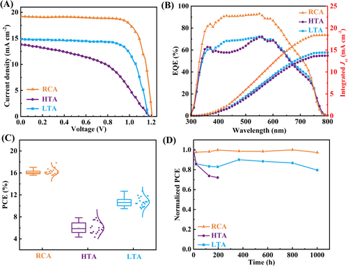
The inverted PSCs with an architecture of ITO/NiOx/PTAA/(4FPEA)2(MA0.9FA0.1)3Pb4I13/PCBM/BCP/Ag are fabricated. The photovoltaic performance of PSCs based on RCA, HTA, and LTA is firstly investigated by J-V curves, as shown in Figure 4A. Generally, photovoltaic parameters include Jsc, open-circuit voltage (Voc), fill factor (FF), and PCE. It is found that the champion PCE of the RCA-based PSC is up to 17.8% with a Voc of 1.21 V, a Jsc of 19.19 mA cm−2, and a FF of 76.45%. The Voc, Jsc, FF, and PCE of the LTA-based PSC are 1.17 V, 14.92 mA cm−2, 72.81%, and 12.7%, respectively. The HTA-based PSC shows a low PCE of 7.8% (Voc = 1.18 V, Jsc = 13.85 mA cm−2, and FF = 47.91%). The main reason for the increase in FF is the improved crystal quality of the RCA-based perovskite film.41 The Voc value achieves 1.21 V, which can be attributed to the small non-radiative Voc loss. Importantly, the RCA-based PSC exhibits the highest Jsc value, due to the high-quality perovskite film grown along the out-of-plane direction. From Figure S7, the RCA- and LTA-based PSCs exhibit the less hysteresis index. Furthermore, the Jsc value can be proved by EQE spectra, as shown in Figure 4B. The integrated current densities of PSCs based on RCA, HTA, and LTA are 18.36, 13.77, and 14.41 mA cm−2, respectively.42 The calculated Jsc values are consistent with the J-V curves. Figure 4C and Figure S8 show the statistical distribution of photovoltaic parameters of PSCs based on RCA, HTA, and LTA. The RCA-based PSC exhibits very well repeatability for 20 devices. Figure S9 shows the steady-state output of PSCs based on RCA, HTA, and LTA at a maximum power point for 200 s. The steady-state output for photocurrent density of PSCs based on RCA, HTA, and LTA are 17.87, 9.56, and 13.61 mA cm−2, respectively. The corresponding stable PCEs are 17.7% (Vmax at 0.99 V), 7.7% (Vmax at 0.81 V), and 12.9% (Vmax at 0.95 V), respectively. The RCA-based PSC displays good illumination stability. Then, the long-term stability of PSCs without encapsulation stored in a nitrogen-filled glove box is shown in Figure 4D. The HTA-based PSC remains only 72.1% of its original PCE after 195 h. Meanwhile, the PCE of the LTA-based PSC remains 79.7% of its original PCE after 1000 h. Especially, the RCA-based PSC has excellent long-term stability and remains 97.4% of the initial PCE after 1000 h.
3 CONCLUSION
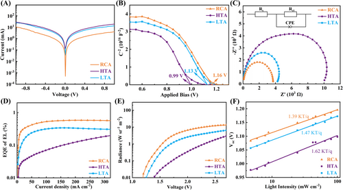
In conclusion, our study has successfully demonstrated the reverse-cool annealing strategy for the fabrication of high-quality 2D RP perovskite films with preferred growth along the out-of-plane direction. These 2D RP perovskite films exhibit a compact and pinhole-free morphology, which significantly reduces defects and enhances charge transport capabilities. Consequently, 2D RP PSCs display a high charge carrier extraction efficiency and a minimal non-radiative open-circuit voltage loss (149 mV). The leading 2D RP PSC in our research achieved an outstanding PCE of 17.8%. Furthermore, the long-term stability of these PSCs, even when stored in a nitrogen environment for over 1000 h, showed no significant deterioration. Our work introduces a promising annealing strategy to produce high-performance 2D RP perovskite films, paving the way for the advancement of 2D PSCs in practical applications.
4 METHODS
4.1 Materials
Polymer polybis(4-phenyl)(2,4,6-trimethylphenyl)amine (PTAA, molecular weight: 1000–10 000 g mol−1), 4-fluorophenylethylammonium iodide (4FPEAI, 99%), lead (II) iodide (PbI2, 99.9%), methylammonium chloride (MACl, 99.5%), formamidinium iodide (FAI, 99.5%), methylammonium iodide (MAI, 99.9%), lead(II) chloride (PbCl2, 99.9%), 2,9-dimethyl-4,7-diphenyl-1,10-phenanthroline (BCP, 99%), 6,6-phenyl C61 butyric acid methyl ester (PCBM, 99%), 2,2′,7,7′-tetrakisN, N-di(4-methoxyphenyl)amino-9,9′-spirobifluorene (Spiro-OMeTAD, ≥99.5%), 4-tert-Butylpyridine (TBP, >96%), and lithium bis(trifluoromethanesulphonyl)imide (LiTFSI, >99%) were purchased from Xi'an polymer light technology Corp. N, N-dimethylformamide (DMF, 99.8%), dimethyl sulfoxide (DMSO, 99.9%), chlorobenzene (CB, 99.8%), Isopropyl alcohol (IPA, 99.8%), and acetonitrile (99.9%) were purchased from Sigma-Aldrich. Ammonium hydroxide (NH4OH, 25.0%–28.0%) purchased from Sinopharm Chemical Reagent Co., Ltd. Acetylacetone (C5H8O2, 99%) and 2-methoxyethanol (C3H8O2, 99.3%) were purchased from Alfa Aesar. Nickel (II) nitrate hexahydrate (Ni(NO3)2·6H2O, 98%) was purchased from Shanghai Aladdin Biochemical Technology Co., Ltd. All the materials were used directly without further purification.
4.2 Preparation of precursor solutions
NiOx precursor solution was prepared by dissolving 290.79 mg of Ni(NO3)2·6H2O in 10 mL of 2-methoxyethanol and then adding 100 μL of ammonium hydroxide and 100 μL of acetylacetone, respectively. PTAA solution with 2 mg mL−1 was obtained by dissolving PTAA in CB at room temperature. 2D RP perovskite (4FPEA)2(MA0.9FA0.1)3Pb4I13 (n = 4) precursor solution with 1.1 M was prepared by dissolving 14.2 mg of FAI, 118.0 mg of MAI, 507.1 mg of PbI2, 7.5 mg of MACl, 30.6 mg of PbCl2, and 147.1 mg of 4FPEAI in a solution including 50 μL of DMSO and 950 μL of DMF. PCBM solution with 20 mg mL−1 was obtained by dissolving PCBM in CB at room temperature. BCP solution with 0.5 mg mL−1 was obtained by dissolving BCP in IPA at room temperature. Spiro-OMeTAD precursor solution was prepared by dissolving 56.4 mg of Spiro-OMeTAD, 22.6 μL of TBP, and 14.04 μL of LiTFSI (520 mg mL−1 in acetonitrile) into 780 μL of CB.
4.3 Device fabrication
The cleaned indium tin oxide (ITO) glasses were treated with ultraviolet-ozone for 15 min. NiOx films were synthesized by spin-coating NiOx precursor solution on ITO glasses at 4000 rpm for 30 s and heating at 250 °C for 40 min. Then, NiOx films were transferred into the glove box with nitrogen. NiOx/PTAA films were obtained by spin-coating PTAA solution on NiOx films at 5000 rpm for 60 s and heating at 100 °C for 10 min. 2D RP perovskite (4FPEA)2(MA0.9FA0.1)3Pb4I13 (n = 4) precursor solution was spin-coated on NiOx/PTAA film at 5000 rpm for 15 s. After that, the wet film was sequentially annealed at 120 °C for 8 s and 80 °C for 5 min. The as-fabricated process of 2D RP perovskite films was defined as RCA. Meanwhile, 2D RP perovskite films were also fabricated by annealing at 120 °C for 5 min (HTA) or 80 °C for 5 min (LTA). In the following step, the PCBM solution was spin-coated on 2D RP perovskite films at 2500 rpm for 60 s and heated at 80 °C for 10 min. BCP solution was also spin-coated at 3500 rpm for 30 s and heated at 80 °C for 10 min. At last, a thermal evaporation system was used to prepare an Ag electrode with 70 nm.
4.4 Measurement and characterization
The scanning electron microscope (SEM, Quanta 250 FEG) and atom force microscope (AFM, Bruker Dimension Icon) was used to character the morphology and roughness of 2D RP perovskite films. The X-ray diffraction (XRD, D8 DISCOVER) and grazing-incidence wide-angle X-ray scattering (GIWAXS, Xeuss 2.0 SAXS/WAXS system) were used to analyze the phases and crystal direction of 2D RP perovskite films. Cu X-ray source (8.05 keV, 1.54 Å) and a Pilatus3R 300 K detector were used for the GIWAXS measurement. The incident angle was set as 1 °. In photoluminescence (PL) system, a continuous-wave solid state laser with wavelength of 447 nm was used as the excitation pump. The signal was collected by an optical fiber coupled CCD spectrometer. For the time-resolved PL (TRPL) measurements, the expectation was use a Q-switched Nd:YAG pulsed laser (532 nm, the pulse duration is about 350 ps with repetition rate of 50 Hz) for excitation intensity of 1 μJ cm−2. The PL signal was detected by 1 GHz Si amplified photodetector, which was connected to a 1 GHz digital oscilloscope. The UV–vis–NIR spectrophotometer (UV-3600, Shimadzu) was used to characterize the absorption spectra of 2D RP perovskite films. The in situ absorption test system comprises a xenon lamp (7ILX150, Beijing 7-Star Optical Instruments Co., Ltd.) and a spectrometer (PG2000-Pro, Shanghai Ideaoptics Corp., Ltd). The dark current–voltage curves, electrochemical impedance spectra (EIS), and Mott-Schottky (M-S) curves of 2D RP PSCs were characterized by CHI660E electrochemical workstation. Trap state density and charge mobility of the symmetrical devices were analyzed by the space-charge-limited current (SCLC). The structure of the symmetrical devices was ITO/NiOx/PTAA/(4FPEA)2(MA0.9FA0.1)3Pb4I13/Spiro-OMeTAD/Ag. The external quantum efficiency (EQE) of 2D RP PSCs was measured by the QE-R system (EnliTechnology Co., Ltd.). The luminance and electroluminescence (EL) spectra of 2D RP PSCs was measured by a luminance meter (Konica Minolta, CS-200) and Flame spectrometer (Ocean Optic), respectively. The PCE of 2D RP PSCs was calculated through current density-voltage (J-V) curves, which were obtained by Keithley 2450 source meter under standard sunlight (AM 1.5 G, 100 mW cm−2). The standard sunlight was obtained from the solar simulator (CHF-XM-500 W, Beijing perfectlight Technology Co., Ltd.) and calibrated by irradiance meter (FZ-A). The unencapsulated 2D RP PSCs were stored in a nitrogen atmosphere under dark conditions for long-term stability measurement.
AUTHOR CONTRIBUTIONS
Zhongqi Xie: Investigation, Writing – original draft. Qing-Song Jiang: Supervision, Writing – review & editing. Ya Zhao: Validation. Ligang Yuan: Data curation. Keyou Yan: Methodology. Yong Peng, Huiming Luo, Mojtaba Abdi-Jalebi: Supervision, Writing – review & editing.
ACKNOWLEDGMENTS
This work was financially supported by National Natural Science Foundation of China (No. 61804062), the open research fund of State Key Laboratory of Advanced Technology for Materials Synthesis and Processing (Wuhan University of Technology) (No. 2023-KF-21), and the open research fund of State Key Laboratory of Organic Electronics and Information Displays (No. SKL2023004). The authors thank support from The Chinese University of Hong Kong for GIWAXS. M. Abdi-Jalebi acknowledges Cambridge Materials Limited for its funding and technical support. M. Abdi-Jalebi acknowledges the Department for Energy Security and Net Zero (Project ID: NEXTCCUS), University College London's Research, Innovation and Global Engagement, Cornell-UCL Global Strategic Collaboration Awards, and University of Sydney-University College London Partnership Collaboration Awards for their financial support. M. Abdi-Jalebi acknowledges the ACT program (Accelerating CCS Technologies, Horizon2020 Project No. 691712) for the financial support of the NEXTCCUS project (project ID: 327327). M. Abdi-Jalebi wishes to acknowledge the support of the Henry Royce Institute for Advanced Materials through the Industrial Collaboration Programme and MATcelerateZero, funded from a grant provided by the Engineering and Physical Sciences Research Council EP/X527257/1. This work was supported by the Henry Royce Institute for advanced materials through the Equipment Access Scheme enabling access to the Royce SEM-FIB Suite at Cambridge; Cambridge Royce facilities grant EP/P024947/1 and Sir Henry Royce Institute - recurrent grant EP/R00661X/1. H. Luo is grateful for the support from the Chinese Scholarship Council (CSC) and the Faculty of Mathematical & Physical Sciences (MAPS) at University College London (UCL).
CONFLICT OF INTEREST STATEMENT
Huaiyin Institute of Technology of China has submitted patent applications related to the subject to Chinese National Intellectual Property Administration on 16 Dec. 2022 (CN 202211621354.9), the authors are part of inventors.


