Minimizing voltage losses in Sn perovskite solar cells by Cs2SnI6 passivation
Jin Hyuck Heo and Sang Woo Park contributed equally to this work.
Abstract
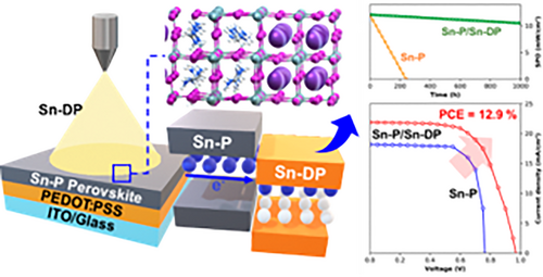
Stability and oxidation are major bottlenecks in improving the performance of Sn-based perovskite solar cells. In this study, we present the formation of an n-type Cs2SnI6 double-perovskite (Sn-DP) layer on a (PEAI)0.15(FAI)0.85SnI2 perovskite (Sn-P) layer using an orthogonal solution-processable spray-coating method. This novel approach achieves a minimized Voc loss of 0.38 V and a PCE of 12.9% under 1 sun conditions. The n-type DP layer effectively passivates tin vacancies, suppresses Sn2+ oxidation, reduces defects, and enhances electron extraction. Furthermore, the Sn-DP/Sn-P-based solar cells exhibit excellent light-soaking stability for 1000 h in the air under continuous one sun illumination, which is attributed to the stable Sn4+ state of the DP layer. Our experimental and theoretical investigations reveal that the type-II band alignment between Sn-DP and Sn-P enhances the stability of the solar cells. The proposed Sn-DP/Sn-P architecture offers a promising pathway for developing Sn-based solar cells.
1 INTRODUCTION
Metal halide perovskites (MHPs) have attracted great attention for a decade because their power conversion efficiencies (PCE) reached over 26.1% at 1 sun condition since Kojima et al. reported 3.8% of liquid junction methylammonium lead trihalide (MAPbX3: X = Br and I)-solar cells (SCs).1, 2 However, the MHP-SCs with high efficiencies intrinsically have toxic lead, and consequently, their applications to common electric and electronic appliances as power sources seem to be restricted.3 In addition, Pb-based MHPs do not have an ideal bandgap (Eg) of 1.34 eV to achieve the Shockley-Queisser (S-Q) theoretical efficiency limit for single-junction SCs because, at best, the Eg of formamidinium lead triiodide (FAPbI3) is ~1.48 eV.4-7
Accordingly, the Sn-based MHPs have been intensively studied because their Eg (1.2–1.4 eV) are ideal for high-efficiency single-junction SCs.8-11 Despite extensive studies for the development of stable and high-efficiency Sn-based MHP-SCs, their stabilities and efficiencies remain inferior to the Pb-based MHP-SCs because the Sn-based MHPs can be easily oxidized to Sn4+ by exposure to air and have two-three folds higher open-circuit voltage (Voc) loss than the Pb-based MHPs.12-14 The Voc loss (Eg − Voc) in the Sn-based MHPs is attributed to the non-radiative recombination by bulk and interface defects, which are created by the oxidation of Sn and quicker crystallization rate.15-17 Therefore, reducing Voc loss in Sn-based MHP-SCs is crucial to developing stable and efficient Pb-free MHP-SCs. This can be achievable only by minimizing defects and preventing oxidation in the Sn perovskites. To minimize Voc loss, the defects in FASnI3 MHPs have been reduced by introducing additives such as piperazine,18 phenethylammonium thiocyanate (PEASCN),19 ethylenediamine diiodide,20 piperazine dihydriodide,21 reducing phenylhydrazine cation halogen,22 and GeI2 doping.23 In addition, to further enhance the Voc in FASnI3 MHP-SCs, Jiang et al. replaced PCBM ([6,6]-phenyl-C61-butyric acid methyl ester) electron transporting layer (ETL) with ICBA (indene-C60 bisadduct) ETL in (PEASCN)0.15(FAI)0.85SnI2 MHP-SCs and attained Eg (1.39) − Voc (0.94) = 0.45 V (see Table S1 for Eg − Voc of representative Sn-based MHP-SCs).24
Although the n-type Cs2SnI6 double perovskite (DP) is known to have much better air stability than the FASnI3 perovskite because it is composed of a stable Sn4+ state,25; however, it has not yet been used as an electron extraction layer or passivation layer for n-i-p- or p-i-n-type FASnI3 MHP-SCs. Zhang et al. deposited n-type Cs2SnI6 via vacuum process on p-type CsSnI3 perovskite and demonstrated 1.1% of n-p heterojunction (HJ) MHP-SCs.26 Here, we formed n-type Cs2SnI6 DP on (PEAI)0.15(FAI)0.85SnI2 perovskite layer via orthogonal solution-processable spray-coating for the first time and attained the minimum Eg (1.35) − Voc (0.97) = 0.38 V. Through the minimization of Voc loss, the Sn-based MHP-SC showed 12.9% of PCE at 1 sun condition because the n-type Cs2SnI6 DP layer passivates Sn vacancy, suppresses oxidation of Sn2+, reduces defects, and improves electron extraction. In addition, the encapsulated Sn-based MHP-SCs passivated by a Cs2SnI6 DP layer with a stable Sn4+ state exhibited good light-soaking stability for 1000 h in air under continuous illumination with one sun.
2 RESULTS AND DISCUSSION
To compare the properties of the PEA0.15FA0.85SnI3 perovskite (Sn-P) and Cs2SnI6 double perovskite (Sn-DP), Sn-P and Sn-DP films were fabricated by spin-coating and ultrasonic spray-coating process in an N2 charged glove box, respectively. Here, the orthogonal processable spray-coating formed the Sn-DP film to create the Sn-DP layer on top of the Sn-P layer.27 The Sn-P and Sn-DP films were prepared by using 0.8 M PEAI:FAI: SnI2:SnF2 (0.15:0.85:1:0.075) in DMF: DMSO (4:1) solution and 0.3 M CsI: SnI4 in DMF solution with 10 volume part of HI solution. Their scanning electron microscopy (SEM) images are shown in Figure 1A,B. The Sn-P film had large crystal domains without pinholes, whereas the Sn-DP film had small crystal grains. The corresponding x-ray diffraction (XRD) patterns in Figure 1C indicate that no detectable impurity peaks appear, and consequently, pure Sn-P and Sn-DP crystalline phases are well formed.24, 28 However, the XRD patterns cannot guarantee the formation of pure Sn-P and Sn-DP films because oxidized Sn can form amorphous SnO2.29 Therefore, we confirmed the uniform formation of the Sn-P and Sn-DP layers through grazing incidence x-ray diffraction (GIXRD) measurements (Figure S1A). Our results showed that, at the lowest incident angle of 0.1°, the XRD pattern closely matched that of Sn-DP. As the incident angle increased, the intensity of the Sn-P peaks gradually increased, while the Sn-DP peaks decreased. At an incident angle of 0.9°, the XRD pattern closely aligned with that of Sn-P. Furthermore, as no new peaks appeared with increasing incident angles, which confirmed that the Sn-DP spray-coating did not affect the crystal structure of either the Sn-DP or Sn-P layers.
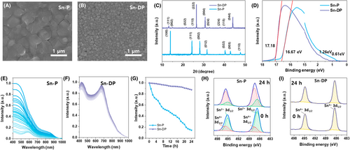
To understand the band structure of each material, the UV–visible absorption spectra were measured, as shown in Figure S1B. The onset absorptions of the Sn-P and Sn-DP films were approximately 920 and 870 nm, respectively. Their electronic band gaps were calculated from Tauc plots as shown in Figure S1C, of which the Sn-P and Sn-DP films had ~1.35 eV and ~1.42 eV, respectively. Their electronic energy states were analyzed using ultraviolet photoelectron spectroscopy (UPS), as shown in Figure 1D. The valence band maximum energy level (EVBM = hν − Ecut-off + ΔEVB, where hν = 21.22 eV for He I) of Sn-P and Sn-DP films were 5.16 eV and 5.30 eV, respectively, where the corresponding Ecut-off and ΔEVB are 17.18 eV and 1.26 eV for Sn-P film and 16.67 eV and 0.61 eV for Sn-DP film.
To evaluate the stability of Sn-P and Sn-DP films against the external environment, the unencapsulated Sn-P and Sn-DP films were exposed in air at 25°C/20% of relative humidity condition for 24 h. The UV–visible absorption spectra of the Sn-P and Sn-DP films were recorded with increasing exposure time, as shown in Figure 1E,F. The absorbance of the Sn-P film gradually decreased owing to the oxidation of Sn2+ to Sn4+, whereas the Sn-DP film did not show a significant degradation in absorbance. The normalized absorption intensity evolution at 550 nm with exposure time is plotted in Figure 1G. This indicates that the Sn-P film showed poor stability against air, whereas the Sn-DP film has good stability.
For a detailed analysis of the purity and stability of the Sn-P and Sn-DP films, their x-ray photoelectron spectroscopy (XPS) spectra were obtained, as shown in Figure 1H,I, respectively. The spectrum at the bottom represents the XPS data taken at the initial stage (exposure time = 0 h). In contrast, the spectrum at the top, labeled “24 h,” illustrates the changes in the electronic environment of the tin at the final stage (exposure time = 24 h). The Sn-DP film exhibited the pure Sn4+ 3d3/2 peak at 494.90 eV and the pure Sn4+ 3d5/2 peak at 486.50 eV.30 In contrast, the Sn-P film exhibited the Sn2+ 3d3/2 and 3d5/2 peaks at 495.1 eV and 486.70 eV, and the Sn4+ 3d3/2 and 3d5/2 peaks at 495.7 eV and 487.50 eV, respectively.24 Although both films were fabricated in a glove box, the Sn-P film tends to quickly oxidize compared with the Sn-DP film during the analysis because it is composed of Sn2+, while Sn-DP is composed of Sn4+. Therefore, XPS analysis confirmed that the Sn-P film contained oxidized Sn impurities, whereas the Sn-DP film did not.
The XPS spectra of the Sn-P film (Figure 1H) indicate that the Sn2+ peaks appeared predominantly at the beginning (0 h); however, after 24 h of exposure to air (24 h), the Sn4+ peaks became dominant because of the severe oxidation of Sn2+ to Sn4+. The compositions of Sn2+ and Sn4+ in the initial and final stages are summarized in Table S2. The ratio of Sn4+ to Sn2+ in the Sn-P film was 0.28 at the initial stage and increased greatly to 3.23 at the final stage. Accordingly, the Sn-P film showed poor air stability due to quick oxidation. In contrast, the XPS spectra of the Sn-DP film (Figure 1I) showed pure Sn4+ peaks even after 24 h of exposure to air because it was composed of Sn4+. This implies that if an Sn-DP layer is formed on top of the Sn-P film, the Sn-P/Sn-DP film can exhibit good stability against the external environment.
For the fabrication of Sn-P- and Sn-P/Sn-DP-based SCs, the Sn-P device was composed of ITO/PEDOT: PSS/Sn-P/CPTA/BCP/Ag and the Sn-P/Sn-DP-30 s (spray-coating time = 30 s) device was composed of ITO/PEDOT: PSS/Sn-P/Sn-DP-30 s/CPTA/BCP/Ag. An SEM cross-sectional image of the Sn-P-based solar cell is shown in Figure 2A, indicating that the thickness of the Sn-P film was ~400 nm. The corresponding time-of-flight secondary ion mass spectrometry (ToF-SIMS) depth profiles of each component are shown in Figure 2B, confirming that all layers were distinctively formed. Figure 2C shows an SEM cross-sectional image of a Sn-P/Sn-DP-30 s-based solar cell showing that an additional ~50 nm-thick Sn-DP layer is formed on top of the ~360 nm-thick Sn-P layer. The corresponding ToF-SIMS depth profiles of each component in Figure 2D indicate that all the layers were distinctively formed; however, Sn-P and Sn-DP were intermixed in the Sn-DP layer while forming a graded compositional profile. The exact compositional profile of the Sn-DP layer was unclear. The relatively bulkier PEA intermixed less with the Sn-DP layer than the FA and Sn-DP layers. In addition, both the FA and PEA profiles suggest that the Sn-DP layer was well formed on the Sn-P layer because of the low intensities of FA and PEA in the Sn-DP layer.
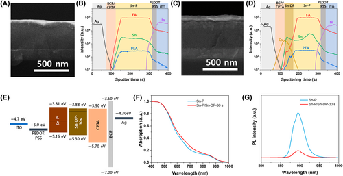
The corresponding energy band diagram of the device is shown in Figure 2E, which indicates that the charge carriers generated in the Sn-P and Sn-P/Sn-DP layers can be energetically transported to the electrode. The measured Fermi levels of Sn-P and Sn-DP were ~ 4.55 eV and ~ 4.04 eV, respectively. Therefore, the generated electron–hole pairs in the Sn-P layer can be efficiently dissociated owing to the type-II band alignment at the Sn-P/Sn-DP interface.
The absorption spectra of the Sn-P and Sn-P/Sn-DP-30 s films in Figure 2F show that both films have the same onset absorption band edge at ~920 nm. The static photoluminescence (PL) spectra of both films are shown in Figure 2G. The Sn-P/Sn-DP film exhibits greater PL quenching than the Sn-P film. This confirms that the generated electron–hole pairs dissociated at the Sn-P/Sn-DP interface. Hence, the Sn-DP layer acted as a charge separation and passivation layer. Here, we controlled the thickness of the Sn-DP layer on the Sn-P film formed by the spin-coating process with spray-coating times (15, 30, and 45 s). The SEM surface images, UV–visible absorption spectra, static PLs spectra, UPS spectra, and XPS spectra are shown in Figure S2.
The photovoltaic properties of the Sn-P- and Sn-P/Sn-DP-30 s-based SCs under one sun (100 mW/cm2) conditions are shown in Figure 3A,B, respectively. The best Sn-P device showed 0.73 V of open-circuit voltage (Voc), 18.15 mA/cm2 of short-circuit current density (Jsc), 74.28% fill factor (FF), and 9.84% PCE at forward scan condition and 0.74 V of Voc, 18.19 mA/cm2 of Jsc, 76.23% of FF, and 10.26% of PCE at reverse scan condition. In contrast, the best Sn-P/Sn-DP-30 s device had 0.96 V of Voc, 20.89 mA/cm2 of Jsc, 62.15% of FF, and 12.46% of PCE at forward scan condition and 0.97 V of Voc, 20.93 mA/cm2 of Jsc, 63.74% of FF, and 12.94% of PCE at reverse scan condition. The certified Sn-P/Sn-DP-30 s device had 0.959 V of Voc, 20.88 mA/cm2 of Jsc, 61.7% of FF, and 12.37% of PCE, as shown in Figure S3. The J-V curves of the best devices for Sn-P, Sn-P/Sn-DP-15 s, Sn-P/Sn-DP-30 s, and Sn-P/Sn-DP-45 s, and the average photovoltaic parameters of 50 samples for each device are shown in Figure S4. The photovoltaic parameters are summarized in Table S3. The external quantum efficiency (EQE) spectra of the Sn-P and Sn-P/Sn-DP-30 s samples in Figure 3C indicate that the Sn-P/Sn-DP-30 s device has a better charge separation and charge collection efficiencies than the Sn-P device because the EQE is a product of the light-harvesting, charge separation, and charge collection efficiencies.

To understand why the Sn-P/Sn-DP-30 s sample exhibited better performance than the Sn-P sample, the photovoltage decay (Figure S5A), photocurrent decay (Figure S5B), and capacitance-voltage (C-V) curves (Figure 3D) were measured. The photovoltage decay curves indicate the carrier recombination time (τrec) is ~3.4 μs for the Sn-P device and ~ 4.7 μs for Sn-P/Sn-DP-30 s device. The photocurrent decay curves indicate that the charge transfer time (τtr)/the corresponding diffusion coefficient (Dn) of Sn-P and Sn-P/Sn-DP-30 s sample is ~1.4 μs/4.49 × 10−4 cm2/s and ~ 1.2 μs/6.63 × 10−4 cm2/s, respectively. Accordingly, the carrier diffusion lengths (Ln) were ~ 370 and ~ 560 nm for the Sn-P and Sn-P/Sn-DP-30 s samples, respectively. This confirms that the Sn-P/Sn-DP-30 s sample exhibits better charge transfer and recombination than the Sn-P sample because the Sn-DP layer on the Sn-P film enhances charge separation and extraction, thereby increasing Jsc and Voc. From the C-V curves of Sn-P and Sn-P/Sn-DP-30 s sample under dark conditions (Figure 3D),19, 21-23 we obtained that the total concentration of impurities of Sn-P and Sn-P/Sn-DP-30 s sample are ~1.16 × 1017 cm−3 and ~ 5.23 × 1016 cm−3, respectively. Therefore, the trap density of the Sn-P/Sn-DP-30 s sample was ~two times lower than that of the Sn-P sample. The abscissa intercepts of the linear regimes in the Mott-Schottky plots indicate that the built-in potential of Sn-P and Sn-P/Sn-DP-30 s sample is ~0.52 V and ~ 0.7 V, respectively. Therefore, the Sn-DP layer on the Sn-P film can enhance charge transfer and reduce recombination and trap density, thereby considerably enhancing the performance of the device.
Oxidation is notorious for presenting a significant challenge to the long-term stability of Sn perovskite SCs. Figure 4 shows the stability test of unencapsulated and encapsulated Sn-P and Sn-P/Sn-DP-30 s devices under continuous illumination of one sun condition in an ambient environment (temperature 25°C/relative humidity 20% ~ 25%). The performance was measured every 10 h with the PCE values shown in Figure 4A,D. For the unencapsulated Sn-P device, the PCE value significantly decreased within 3 min from the initial PCE value of 9.69% to 0.04%, with the corresponding J-V curves depicted in Figure 4C. The unencapsulated Sn-P/Sn-DP 30 s device took 26 min to lose its initial efficiency, from 12.04% to 0.09%, with J-V curves shown in Figure 4B. Consequently, the Sn-P/Sn-DP 30 s device was confirmed to be more than eight times more stable in air than the Sn-P device. Therefore, the stability test under air exposure proves(suggests) that the Sn-DP layer on the Sn-P layer inhibits direct contact with oxygen in the Sn-P layer and prevents rapid corrosion of the Sn-P layer, thereby improving the device stability. Figure 4E shows that the encapsulated Sn-P/Sn-DP 30-s device maintained its stability for 1000 h without significant PCE value reduction, from 12.33% to 10.26%. In contrast, the encapsulated Sn-P device exhibited a sharp PCE drop from 9.77% to 0.03% over 130 h. Even under encapsulation, the Sn-P.
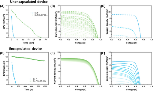
Device shows inferior stability to the Sn-P/Sn-DP-30 s device as shown in Figure 4D,F.
The crystal structure of Cs2SnI6 (Sn-DP) was elucidated using the lattice of CsSnI3 as the foundational framework. Figure S6A illustrates a 2 × 2 × 2 superlattice of CsSnI3, where the cyan, gray, and purple spheres represent Cs, Sn, and I atoms, respectively, forming a cubic perovskite structure. The removal of the selected Sn atoms (highlighted in yellow in Figure S6B) induces an ordered vacancy structure in CsSnI3, which coincides with the crystal structure of Cs2SnI6 (Figure S6C). This structural coherence between the Sn-DP and conventional perovskite structures can be beneficial for forming efficient interfacial structures.
Although the growth of high-purity Sn-DP requires careful process control, the Sn-DP structure is energetically stable.31 To verify the stability of the Sn-DP structures, we calculated the formation energies of various vacancy configurations of Cs2SnI6, whose lattice structures are shown in Figure S7. Figure 5A shows that the Sn-DP structure showed the lowest formation energy among the considered Cs2SnI6 compounds, indicating that the ordered vacancy structure (Sn-DP) is the most favorable lattice structure because of the strong Coulombic interactions between the Sn4+ cations. Therefore, disordered structure formation can be disregarded when phase-pure Sn-DP can be synthesized, as shown in Figure 1C,I.
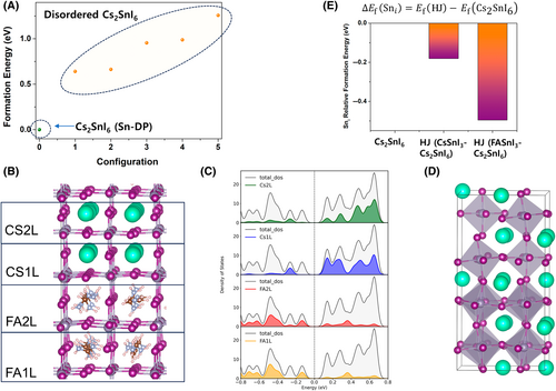
To investigate the electronic structure of Sn-DP/Sn-P, we modeled a superlattice consisting of FASnI3 and Cs2SnI6 as shown in Figure 5B. The resulting projected density of states (PDOS) showed no trap states within the bandgap (Figure 5C), which also presents the valence band maximum. The conduction band minimum consists of the molecular orbitals of FASnI3 and Cs2SnI6, as expected from our XPS analysis (Figure 2E). Considering the reported defect formation energies,31 the Sn interstitials (Sni) could be one of the origins of the n-type semiconducting behavior of Cs2SnI6, because our devices were made of Sn-DP/Sn-P junctions. Cs2SnI6 was under Sn-fluent conditions. The formation energies Ef were calculated for pure Cs2SnI6 (reference value), the Cs2SnI6/CsSnI3 superlattice (Figure 5D), and the Cs2SnI6/FASnI3 superlattice. The relative formation energies (subtracting the formation energy of Sni of Cs2SnI6 from that of the HJ) decrease for the HJ structures (Figure 5E). The interface energy also follows a similar trend. We calculated the interface energy (Einterface) of the Sn-DP/Sn-P HJ structure shown in Figure 5B using the following equation: Einterface = ((EHJ − (ECs2SnI6 + EFASnI3))/Ainterface (Å2)), where EHJ is the energy of HJ. The calculation results confirmed that the Sn-DP/Sn-P HJ is more energetically stable, with an interface energy of −0.0274 eV/Å2. This demonstrates that the n-type characteristics of Sn-DP can be promoted by forming HJs with Sn-rich perovskites.
3 CONCLUSION
We successfully demonstrated the formation of an n-type Sn-DP on a Sn-P using an orthogonal solution-processable spray-coating for the first time. This approach minimizes the Voc loss to 0.38 V and achieves a PCE of 12.9% under 1 sun condition. The Sn-DP layer effectively passivated the vulnerable tin-based perovskite surfaces, suppressed the oxidation of Sn2+, and reduced defect formation. Owing to the stable Sn4+ state of DP, the Sn-DP/Sn-P-based SCs exhibited excellent light-soaking stability for 1000-h in air under continuous illumination. Our experimental and theoretical investigations revealed that the type-II band alignment between Sn-DP and Sn-P promotes electron transport and blocks the generated holes. The proposed Sn-DP/Sn-P architecture provides a promising pathway for developing highly efficient and stable Sn-based Pb-free SCs.
4 EXPERIMENTAL SECTION
To fabricate Sn-P/Sn-DP-based PSCs, patterned ITO glass substrates were sequentially cleaned by ultrasonication in deionized water, acetone, and isopropanol for 15 min each, followed by drying and UV/ozone treatment for 20 min. Then, a PEDOT: PSS/methanol solution with a 1:1 volume ratio was filtered through a 0.45 μm filter, spin-coated onto the cleaned ITO glass substrate at 3000 rpm for 60 s, then dried at 150°C for 20 min. To form the Sn-P/Sn-DP layer on the PEDOT: PSS layer, a 0.8 M Sn-P precursor solution was prepared by dissolving PEAI, FAI, SnI2, and SnF2 in a ratio of 0.15:0.85:1.0:0.075 in a solvent mixture of DMF and DMSO in a 4:1 volume ratio. 200 μL of the prepared Sn-P solution was dropped on the PEDOT: PSS substrate and spin-coated at 1000 rpm for 10 s and 4000 rpm for 30 s. During spin-coating, 1 mL of diethyl ether was added dropwise for 30 s. After spin-coating, the substrate was annealed at 80°C for 5 min. Subsequently, the Sn-DP layer was deposited by a spray-coating process using 0.3 M Sn-DP precursor solution prepared by dissolving CsI and SnI4 in a 2:1 ratio in DMF and stirring at 50°C for 30 min, and then adding 0.1 mL of HI per 1 mL of the solution. The prepared Sn-DP solution was filtered through a 0.2 μm filter and loaded into a syringe pump for spray-coating. The spray-coating setup included a 120 kHz ultrasonic spray-coating head, a 5 cm distance between the spray head and substrates, a solution feed rate of 0.5 mL/min, and a spray-coating temperature of 80°C. Under these conditions, the Sn-DP solution was spray-coated for 60 s and annealed at 150°C for 5 min. The substrates were then transferred to a thermal evaporator, where CPTA, BCP, and Ag were sequentially evaporated at deposition rates of 0.5, 0.2, and 2.0 Å/s, respectively, to a final thickness of 30, 7, and 100 nm. The deposition area was defined using a shadow mask as 0.16 cm2.
We employed density functional theory (DFT) calculations to investigate the electronic structures and formation energies of the Sn-DP and superlattice structures using the Vienna ab initio simulation package (VASP).32, 33 We adopted the Perdew-Burke-Ernzerhof exchange-correlation functional revised for solids (PBESol). The electronic wavefunctions were expanded using an energy cutoff of 520 eV, and 2 × 2 × 1 Γ-centered k-point sampling of the Brillouin zone was used for the superlattice, 2 × 2 × 2 for Sn-DP. The lattice structures are optimized by relaxing all atomic positions and constants until the residual forces and energy differences fall below 0.01 eV/Å and 10−6 eV, respectively.
The screened hybrid functionals of Heyd, Scuseria, and Ernzerhof (HSE).34 The screening and mixing parameters in the HSE functional were set to 0.2 and 0.2. Atomic structures were visualized using the VESTA package to enhance clarity and understanding.35
AUTHOR CONTRIBUTIONS
Jin Hyuck Heo: Writing of the original draft and investigation. Sang Woo Park: Writing the original draft and computation. Hyong Joon Lee: Investigation. Jin Kyoung Park: Investigation. Sang Hyuk Im: Supervision. Ki-Ha Hong: Supervision.
ACKNOWLEDGMENTS
This study was supported by National Research Foundation of Korea (NRF) grants funded by the Korean government (MSIT) (Grant Nos. 2022R1A2C3004964, 2022R1C1C2008126, 2022M3H4A1A03074093, RS-2023-00257666 and RS-2024-00450836). J. H. Heo acknowledges the support of the Korea Institute of Energy Technology Evaluation and Planning (KETEP) and the Ministry of Trade, Industry & Energy (MOTIE) of the Republic of Korea (No. 20227410100040), as well as the National Research Foundation of Korea (NRF) grant funded by the Korea government (MSIT) (No. 2022R1C1C2008126).
CONFLICT OF INTEREST STATEMENT
The authors declare no conflicts of interest.


