MgSc2Se4 Solid Electrolyte for Rechargeable Mg Batteries: An Electric Field-Assisted All-Solid-State Synthesis
Abstract
Magnesium scandium chalcogenide spinels are an important class of materials in Mg anode-based batteries for energy storage applications. The applications of these intriguing materials are not limited to the energy storage, but the use of these materials may also be useful in solar cells, owing to the material optical bandgap. So far, all reported synthetic routes for these spinels involve high-temperature furnace treatment. Herein, a process which involves a facile electric field-assisted synthesis of MgSc2Se4 is reported on, yielding after a very short thermal treatment, a material possessing a low room-temperature electronic conductivity of ≈10−11 S cm−1, and a room-temperature Mg-ion conductivity of 1.78 × 10⁻⁵ S cm−1. The crucial role of extra selenium on the material electronic conductivity is discussed and explained in detail.
1 Introduction
The role of all-solid-state Mg-ion batteries in the energy storage arena has been increasingly recognized in recent years. This stimulates an intense search for practically viable solid Mg-ion conductors. A low mobility of multivalent Mg ions in solids is the major roadblock in the development of Mg batteries. Until recently, most of the theoretical and experimental studies demonstrated that a high Mg-ion conductivity (≈10−2–10−3 S cm−1) in solids can be achieved at elevated temperatures, starting from 400 °C.[1-7] Recent studies on room-temperature Mg-ion mobility in chalcogenide spinel MgSc2Se4 demonstrated that this material is a promising candidate for an all-solid-state Mg battery, possessing Mg-ion conductivity of ≈10−4 S cm−1.[8-10]
Later on, it was revealed that the material holds too high electronic conductivity (10−5–10−8 S cm−1),[8, 9] and therefore the material would pose problems, once considered as a solid electrolyte in Mg batteries, due to a high electronic current leakage. Recently, a theoretical explanation of this high electronic conductivity was presented by Canepa et al.[11] It was suggested that the origin of the conductivity is an intrinsic doping; particularly, Se dearth in the lattice and Mg/Sc antisites formation were proposed. Whereas the assumption implies that the conductivity may be moderated by saturation of the material with selenium and/or aliovalent doping, Wang et al.[9] reported that an excess of selenium and aliovalent doping does not assist much in reduction of the material's electronic conductivity. Concomitantly, Kundu et al.[10] have demonstrated that the electronic conductivity occurs via the Berthelot-type mechanism, suggesting that the electronic transport occurs through a low-conducting matrix, stuffed with nanoscaled free electron-containing region, being expressed by jumping/tunnelling between these conductive inclusions. It has been demonstrated that metallic-type inclusions, like Sc/ScSe, are more likely to be responsible for the high electronic conductivity of the chalcogenide MgSc2Se4 spinel. Thus, the electronic conductivity of this material was substantially reduced to values of ≈10−11–10−12 S cm−1 by controlling the synthetic parameters.[10] The circumstances suggest again that synthetic parameters and routes are crucial for tuning the properties of the material.
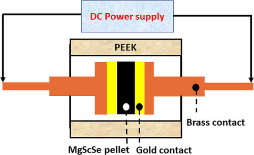
Whereas many synthetic approaches were employed for binary metal selenide preparation,[12] only high-temperature (1000 °C) furnace synthesis in inert atmosphere was reported for ternary metal selenide preparation;[8-10] the processes require a prolonged preparation time of up to 100 h. Regarding MgSc2Se4 spinel, these synthetic routes result in producing a material with an elevated electronic conductivity.[8] These processing conditions make the existing synthetic approaches impractical and generate a great demand for the development of new synthetic routes, enabling a fast, facile, and cost-effective synthesis of the material with enhanced ionic conductivity on one hand, and on the other hand, a reduced electronic conductivity. In the current study, we present a new processing approach, involving a mixing of the elemental precursors (Mg, Sc, and Se powders), preparing a green pellet from this mixture and applying a DC current to the green pellet. As the pellet is conducting, consequently the applied voltage produces current flowing through the pellet. The experimental arrangement bears many similarities to field-assisted sintering (FAST) and spark plasma sintering (SPS),[13] and therefore the occurrence of processes accompanying FAST/SPS (such as charged defect movement, Joule heat evolution, and electrochemical reactions) is expected. These processes are suggested to initiate and facilitate the formation of the MgSc2Se4 chalcogenide spinel. To the best of our knowledge, this is the first ever report on the preparation of MgS2Se4 by electric field-assisted all-solid-state synthesis at room temperature, without an external heating being applied. Mg, Sc, and Se elemental powders (stoichiometric ratio of 1:2:4) were mixed and grounded with a pestle and mortar for about 15–20 min, obtaining homogeneous mixtures. In the next step, a mixture was pressed into pellets (Ø7 mm, ≈0.23–0.36 thick, with an added pinch of Se powder) under a pressure of ≈5.2 kbar for 2–3 min in Ar atmosphere, in a glove box. The pellet was placed inside a two-electrode cell with gold foil contacts on both sides of the pellet, as shown in Scheme 1. Then, the closed cell was transferred into a fume hood and connected to a DC power supply.
2 Results and Discussion
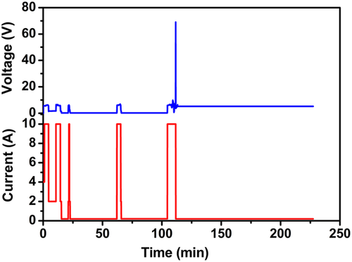
Typically, a DC power was applied to the green pellet according to the description provided in Figure 1. The initial conductivity values of the green pellets are high (as shown in Figure 1): it takes about 6 V to run a current of 10 A through the pellet, implying σpellet ≈ 0.13 S cm−1. Analysis of the electronic conductivity of the pellets provides some insight into the Mg–Sc–Se composite structure. The pellet composed of the Mg/Sc/Se powder mix with the corresponding mole ratio of 1/2/4; thus, the volume ratio of the corresponding components in the pellet is 0.12/0.25/0.63, or 37% of the metals and 63% of selenium. Metal components have prevailingly high conductivity (σMg ≈ 2.3 × 10⁵ and σSc ≈ 1.8 × 10⁴ S cm−1), and therefore a high pellet conductivity is easily comprehended, if it is assumed that the electric current flow through the green pellet via metal pathways formed by contacting metal particles. The existence of such pathways is not feasible in the case of homogeneous powder mixture. Indeed, the least dense noncompressible ball packing (six-coordinated balls) has void volume of ≈0.48, thus selenium cannot be roomed inside the available void volume; actually, it needs more room (extra 15% of the pellet volume). In the case of homogeneous powder mixtures, this circumstance results in the configuration with noncontacting metal particles, and the electric current pathways are expected to include selenium-paved sections. Commercial selenium powder, being a mix of the amorphous and crystalline selenium,[14] has a conductivity σSe in the range of 5.5 × 10⁻¹³–5.25 × 10⁻⁷ S cm−1 at room temperature, and σSe ≈ 10−8 S cm−1 in the liquid state (at the melting point). With reference to Scheme 2, it may be concluded that homogeneous green pellet cannot exhibit initial conductivity as high as 0.13 S cm−1. The abnormally large composite conductivity value may be explained by the existence of a wire-like metal powder structures inside the green pellet body; these conductive pathways (“wires”) are shown in Scheme 3a.

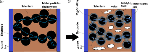
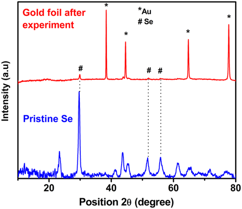
If that is the case, the current is flowing through these wires, and these metal powder “wires” are heated by the Joule heat, flowing by heat emitting into the surrounding selenium. Estimating the average pellet volume as 0.01 cm3, and the metal fraction making up 37% of this volume, the initial 1 min-long current pulse introduces heat energy of ≈100 kJ cm−3. It may be suggested that this energy is enough to melt the selenium fraction of the pellet and even evaporate some selenium. The condensation of this selenium vapors results in the formation of a red selenium film (seen with the unaided eye) onto the gold electrodes during the DC current application. It is interesting that the film formed only on gold electrodes but not on other material electrodes (stainless steel, nickel, etc.). The film composed of crystalline selenium, as presented in Figure 2; the crystalline selenium is a good conductor and is not expected to tamper with the DC current treatment. Currently, we have no reliable information on the specific nature of the mechanism of the spinel crust growth onto Mg/Sc powder, and it can reasonably be argued at this stage that the formation of MgSc2Se4 encounters no difficulty. The distinguished feature of the DC current treatment is that the temperature of the metal fraction and the temperature at the metal–selenium interface are substantially higher than the temperature in the bulk of the selenium fraction; by contrast, the furnace heating suggests that selenium first absorbs the heat irradiated by furnace walls, and thus the temperature at the metal–selenium interface is below the temperature in the bulk of the selenium fraction.
As a result of this difference, the metal–selenium interaction prevails over selenium evaporation, which is advantageous for the spinel formation. In addition, metal particles are covering the Mg–Sc–Se spinel and it may be suggested that Mg and Sc are fused together at contact points of Mg and Sc particles, and selenium reacts with these alloys (Scheme 3b).
The X-ray diffraction (XRD) pattern of the resulting brownish material (containing excess of elemental Se) is similar to the standard MgSc2Se4–XRD pattern (Figure 3c,d). The XRD of the material indicates an excess of crystalline Se; it is also slightly congruently shifted to the left (lower 2θ), once compared with the standard pattern of MgSc2Se4, indicating a larger d-spacing of the prepared sample, if compared with the standard MgSc2Se4 spinel lattice. Optimizing the process to obtain an excess of free crystalline pure Se material was unsuccessful. However, reducing the amount of added Se in the stoichiometric ratio produces different end products like MgSe, Sc2Se3, and other derivatives.
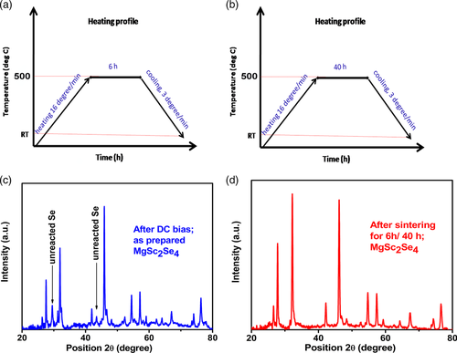
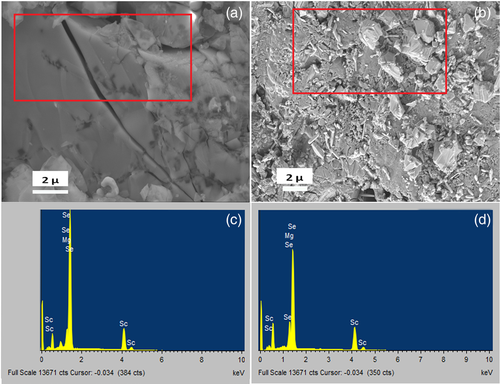
Hence, the produced brownish powder (due to excess Se in the product) was taken out from the cell, grounded in a mortar, and the resulting powder was pressed into pellets, all inside an argon-filled glove box. These pellets were then sintered at 500 °C in an argon atmosphere furnace; two types of the samples were prepared: specifically, some pellets were sintered according to sintering schedule presented in Figure 3a (6 h at 500 C, further designated as samples (a)), and others were sintered according to the sintering schedule presented in Figure 3b (40 h at 500 °C, further designated as samples (b)). The XRD of samples (a) and (b) are similar and both do not demonstrate the presence of selenium; thus, only the XRD of sample (a) is shown in Figure 3. On sintering, the XRDs of both samples shift to the right (higher 2θ), and now it exactly matches the standard XRD of MgSc2Se4, indicating that the heat treatment improves the material crystal structure in a way that its lattice d-spacing exactly matches with the standard pattern of MgSc2Se4 (Figure 3d). Whereas samples (a) maintain brownish color after sintering, sample (b) colors faded and turned to be yellowish. We relate the brownish color of sample (a) to an excess of amorphous selenium, which could not be traced by XRD analysis but was demonstrated by energy dispersive spectroscopy (EDS) analysis. Regarding samples (b), the prolonged heating time eliminated the excess of Se and the yellowish sample (b) was composed of pure MgSc2Se4. The morphology and compositions of the prepared samples are presented in Figure 4. Both sintered pellets (sample (a) and sample (b)) are stacked of 3–4 μm grains. The corresponding EDS data (Figure 4c,d) demonstrate the presence of Mg, Sc, and Se with the atomic ratio of Mg:Sc:Se = 14.7:29.4:68 ≈ 1:2:4.6 in the case of the sample (a), and Mg:Sc:Se = 13.9:27.8:54.6 ≈ 1:2:3.93 in the case of sample (b). The ratios indicate that although XRD does not show the excess of Se, extra selenium is still present in sample (a), whereas sample (b) contains almost a complete stoichiometric amount of selenium. The electrical properties of samples (a) and (b) were studied by electrochemical impedance spectroscopy (EIS) and DC “current versus voltage” measurements; the measurements were conducted with Mg ions blocking gold electrodes. Figure 5a,b shows EIS plots of sample (a) and sample (b), respectively, while Figure 5c presents the corresponding equivalent circuit for the experimental EIS data fitting. The Nyquist plot looks different due to the slight differences in composition. Sample (a) contains slight excess of selenium, playing a crucial role in providing a temperature-dependent electronic conductivity, as discussed earlier. Generally, the impedance response is highly dependent on the composition, surface geometry/structure, nature of grain boundaries, etc. As the main composition is same for both samples and similar ion transport mechanism is expected, the same equivalent circuit has been considered for the fitting (Figure 5c). Sample (a) (Figure 5a) demonstrates a semicircle with an extended linear curve at the low frequencies, associated with diffusion-controlled processes, possibly arising from differences in the structure of the grain boundaries. Such characteristics contribution is not clearly visible for sample (b) (Figure 5b). Hence, both the grain and grain boundary contributions cannot be separated and identified for sample (b) without a fitting in an equivalent circuit (Figure 5c). Thus, electronic conductivity data derived from DC measurements and ionic conductivity data derived from EIS equivalent circuit fitting are tabulated in Table 1 and 2.

| Equivalent circuit element | R | Ω [S cm−1] |
|---|---|---|
| Bulk ionic transport related element | = 55 690 | = 0.163 × 10⁻³ |
| Cross-boundary ionic transport related element | = 512 088 | = 1.775 × 10⁻⁵ |
| Overall ionic transport resistance related value | Rů ≈ 512 088 | Σ ionic ≈ 1.775 × 10⁻⁵ |
| Overall electronic conductivity from DC experiment at room temperature | σ electronic ≈ 3.8 × 10⁻¹⁰ |
| Equivalent circuit element | R | Ω [S cm−1] |
|---|---|---|
| Bulk ionic transport related element | = 50 580 | = 0.179 × 10⁻³ |
| Cross-boundary ionic transport related element | = 480 366 | = 1.89 × 10⁻⁵ |
| Overall ionic transport resistance related value | Rů ≈ 480 366 | Σionic ≈ 1.89 × 10⁻⁵ |
| Overall electronic conductivity from DC experiment at room temperature | σ electronic ≈ 9.3 × 10⁻¹¹ |
The EIS fitting data for sample (a) offer 1.78 × 10⁻⁵ S cm−1 as the value of Mg-ionic conductivity, and DC experiments offer the value of 3.8 × 10⁻¹⁰ S cm−1 (Figure 6) as the electronic conductivity at room temperature.
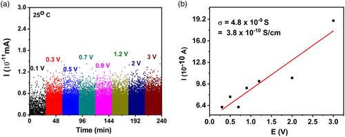
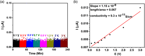
These data, on electronic and ionic conductivity, correlate well with the data reported in our earlier work[10] on MgSc2Se4 prepared by high-temperature synthesis. Regarding sample (b), the EIS fitting data offer 1.9 × 10⁻⁵ S cm−1 as the value of Mg-ionic conductivity, and DC experiments offer 9.3 × 10⁻¹¹ S cm−1 (Figure 7) as the value of the electronic conductivity at room temperature. The calculated electronic conductivity of this sample is 3.8 × 10⁻¹⁰ S cm−1 from the I–V plot (Figure 6), derived from the DC experiments. The electronic conductivity of sample (a) demonstrates a drastic temperature dependence, in the temperatures window of 20 and 60 °C (Figure 5d and Table 3): the conductivity increases in approximately ten orders of magnitude upon heating the sample from 20 to 60 °C. The σDC (T) plot fits well to the Berthelot type curve, suggesting the involvement of nanosized well-conductive inclusions in the conductivity mechanism of the overall insulating material.[10] Good candidates for such conductive inclusions are extra Se (the mole Mg/Sc/Se ratio is actually 1/2/4.5), as the inclusions may be several tenth of nanometers in size. These inclusions appear during sintering as small droplets of liquid selenium (the treatment takes place at 500 °C, whereas selenium melting point is 221 °C). These droplets solidified while cooling down after sintering. The commonly recognized feature of selenium is that its melt is prone to overcooling and usually solidifies as an amorphous (vitreous) body, even under common (moderately fast) cooling.[15]
| T [°C] | T [K] | σ electronic [S cm−1] | lnσe |
|---|---|---|---|
| 20 | 293 | 3.2 × 10⁻¹⁰ | −21.86 |
| 25 | 298 | 3.8 × 10⁻¹⁰ | −21.69 |
| 30 | 303 | 5.7 × 10⁻¹⁰ | −21.54 |
| 40 | 313 | 28 600 × 10−10 | −12.765 |
| 50 | 323 | 41.72 × 10⁻⁵ | −7.782 |
| 60 | 333 | 20.27 | +3.009 |
Thus, these selenium inclusions are expected to be amorphous, having a very low conductivity; the amorphousness of this interstitial selenium inclusion explains the absence of the selenium peak in the XRD pattern of sample (a), whereas EDS detects a noticeable amount of the overstoichiometric selenium. The amorphous selenium inclusions cannot contribute much to the electronic conductivity at room temperature (in the DC measurement), but when it transforms to a crystalline phase, the electronic conductivity might rise by a several order.[14]
Overcooled amorphous selenium easily crystallizes with annealing, though. Particularly, submicrometer selenium particles may be forced to crystallize by annealing at considerably low temperatures, just up to 50 °C. The crystallization takes place with a relatively high amorphous/crystal boundary movement rates (≈10−4–10−5 μm min−1).[16] However, conductivity of the crystalline selenium is many order of magnitude higher than the conductivity of the amorphous selenium (> 10−3 S cm−1 at room temperature[17]). Thus, the temperature enhancement of sample (a) is related to the conversion of nonconductive amorphous selenium inclusions to conductive crystalline selenium inclusions (and putting the Berthelot conductivity mechanism into work). The data presented in Table 4 and in Figure 3(d) demonstrate that contrary to sample (a), the electronic conductivity of sample (b) depends very little on the temperature in the 20–100 °C temperature range. The data presented in Table 4 and in Figure 3d demonstrate that contrary to sample (a), the electronic conductivity of sample (b) depends very little on the temperature in the 20–100 °C temperature range.
| T [°C] | T [K] | σ electronic [S cm−1] | lnσe |
|---|---|---|---|
| 20 | 293 | 9.7 × 10⁻¹¹ | −23.05 |
| 25 | 298 | 9.3 × 10⁻¹¹ | −23.09 |
| 30 | 303 | 8.9 × 10⁻¹¹ | −23.14 |
| 40 | 313 | 1.9 × 10⁻¹⁰ | −22.38 |
| 50 | 323 | 2.46 × 10⁻¹⁰ | −22.12 |
| 60 | 333 | 3.6 × 10⁻¹⁰ | −21.7 |
| 70 | 343 | 4.1 × 10⁻¹⁰ | −21.6 |
| 80 | 353 | 5.2 × 10⁻¹⁰ | −21.37 |
| 90 | 363 | 6.2 × 10⁻¹⁰ | −21.2 |
| 100 | 373 | 11.4 × 10⁻¹⁰ | −20.59 |
This finding is in line with the fact that sample (b) does not contain an extra (overstoichiometric) selenium, and therefore there is little material to form conductive inclusions. Amorphous selenium is a poor conductor, so amorphous selenium nanoinclusions do not impel conductivity to the MgSc2Se4 matrix. Viewed from this perspective, only crystalline selenium should be taken into consideration, if the electronic conductivity of the MgSc2Se4 sample constitutes an essential parameter. On the other hand, although the amorphous selenium is extremely prone to overcooling, sooner or later amorphous selenium crystallizes at room temperature turning to be a conductive stuff; this aspect should also be considered.
3 Conclusions
In summary, we report here on a simple and short synthesis of a chalcogenide MgSc2Se4 spinel, involving room-temperature electric filed-assisted synthesis. This material appears to be promising in advanced rechargeable Mg solid-state batteries applications. The method is providing an easy and fast preparation method of ternary metal chalcogenides, without resorting to high-temperature heat treatments. The electrical properties of the material are studied and discussed in this report. It was found that the electric filed-assisted metal chalcogenide synthesis route may be useful for the preparation of Mg-ion conductive solid electrolytes with a very low electronic conductivity. The following key aspects of the synthetic process should be carefully considered: 1) A correct balance of selenium content in the green precursor pellet should be maintained. The content plays a dual role: on one hand, some of the selenium is lost during the preparation process, and this circumstance requires formulating the green precursor pellet with a certain excess of Se over the stoichiometric amount. On the other hand, extra selenium incorporated into the final product compromises the electronic conductivity of the spinel material. 2) The electric contact material is a matter of a great importance: the point that needs further studies is that among the tested materials, only gold contacts supported the electric filed-assisted synthesis of the spinel. 3) The other significant parameter is the DC current application schedule.
Currently, we are evaluating the electrochemical behavior of this material in all-solid-state Mg battery configuration. The process is tedious, as one needs to control the thickness and the mechanical characteristics of the material. The efforts directed at developing new and advanced processing methods and understanding the effect of these procedures on the microstructure and electrical behavior of the Mg-ionic conductor is vital for the development of an all-solid-state Mg batteries.
4 Experimental Section
Materials
Mg powder, 325 mesh (99.8% purity, Alfa Aesar), Se powder (99% purity, Acros Organics), and Sc (purity: 99.99%, −200 mesh) powder were purchased from SS Technologies and Materials Inc. and gold foil as contact with thicknesses (0.025 and 0.25 mm).
DC Power Supply Specifications
Power station pe4383 ESK, 600 V/10 A, plating electronic GmbH, made in Germany was used for DC power supply.
Pellets Preparation for Electrochemical Characterizations
When the processing was complete, Mg–Sc–Se green pellets turned into loose powder agglomerates, which shattered into powder on cell disassembling. This MgSc2Se4 powder was regrinded with mortar and pestle, pelletized inside a glove box, wrapped with Pt foil, and placed in a quartz crucible.
The crucible with the sample was transferred to the TVF-12NT furnace and heated at 500 °C; some samples were heated for 6 h and some for 40 h, as described in Figure 3a,b, respectively. The sintered pellets were used for DC conductivity and EIS measurements. The theoretical gravimetric density of the material is 4.15 g cc−1. We have used here very thin pellets of less than 0.5 mm in thickness, and they are typically soft unlike oxide-based material pellets. Hence, the relative density calculation using “Archimedes” principle of soaking the material pellet in a suitable liquid can be applied. Moreover, the sulfur or selenium-based materials are more soft and more reactive compared to the oxide-based SEs. Hence, in our case, it was very challenging to find the relative density of the very thin pellets for the measurements.
Materials Characterizations: XRD
XRD of the sample pellets was made by high-resolution diffraction system (Rigaku Smart Lab 9 kW). For this end, the pellet (ø7 mm, 0.26 – 0.38 mm thick) was fixed on top of the glass slide and wrapped with Kapton tape inside an Ar-filled glove box to avoid the sample exposure to the surrounding air; the packed pellet was placed into the diffraction system for XRD measurements. Monochromator and D–tex detector scanning speed was maintained at 2° min−1 in the 2θ range between 20° and 80°.
Scanning Electron Microscopy Imaging and EDS Mapping
Zeiss Ultra-Plus Field Emission Gun (FEG)-scanning electron microscopy (SEM) was used to obtain SEM images and EDS data; the sample pellet was installed into a special home-made stainless-steel holder inside an Ag-filled glove box and the holder with the sample was vacuum-tough sealed in the glove box afterward. The holder design prevented the exposure of the sample to the surrounding air during the transfer of the sample into the SEM working space.
Electrical Characterizations
EIS experiments were performed by MTZ-35 frequency response analyzer (Bio-Logic) in the range between 1 Hz and 4 MHz with a 10 mV AC amplitude. All EIS and DC measurements were conducted in a temperature range of 20 – 100 °C with an Intermediate Temperature System (ITS) measurement cell (Bio-Logic Co.). Mg-ion blocking gold contacts (spring-pressed) were employed in all the EIS and DC measurements using VSP-300 Potentiostat-Biologic with current detection limit 1 pA coupled with ITS.
Synthesis Method and Processing
The detail DC schedule for heating via electric filed-assisted method is described (as per Figure 1) as follows: 1) first, 4 A current pulse is applied for 1 min; 2) then, the first 10 A current is applied for time 10AT1 ≈ 5 min; 3) the first 10 A pulse is followed by the first 2 A current pulse applied for time 2AT1 ≈ 7 min; 4) the first 2 A pulse is followed by the second 10 A current pulse applied for time 10AT2 ≈ 5 min; 5) the second 10 A pulse is followed by the second 2 A current pulse applied for time 2AT2 ≈ 5 min; 6) the second 2 A pulse is followed by the first “rest period,” the current is zero during this period, and it lasts for time t1 ≈ 5 min; 7) the first “rest period” is followed by 2–10–2 A current pulse; 8) the 2–10–2 A current pulse is followed by the second “rest period,” which lasts for time t2 ≈ 34 min; 9) the second “rest period” is followed by the fourth 10 A pulse for time 10AT4 ≈ 3 min; 10) the fourth 10 A pulse is followed by the third “rest period,” which lasts for time t3 ≈ 39 min; 11) the third “rest period” is followed by the fifth 10 A pulse for time 10AT5 ≈ 8 min; at the end of this pulse, the applied voltage reaches 70 V and the sample transition into high resistance state takes place; 12) at this step, the voltage drops down to ≈5–6 V, and the current also drops down to ≈0.2 A, this step lasted for ≈117 min, and the applied power density is around 1217 mW mm−3.
We have also tried to use other materials besides gold for pellet contacts; such materials were selected from Pt, Ni, Mo, and Sn. However, it was found that no other contact materials, but gold could provide the proper conditions for the field-assisted MgSc2Se4 spinel production. It should be emphasized that Pt/Ni/Mo/Sn contacts did not demonstrate any traces of interaction with selenium during the DC current treatment of the samples and these contacts were found intact after the cell was dismantled.
Acknowledgements
This project has received funding from the European Union's Horizon 2020 research and innovation program under grant agreement no. 824066 (E-MAGIC). S.K. would like to acknowledge PBC for granting the PBC postdoctoral fellowship. The authors also appreciate the support of the research by the Israel National Research Centre for Electrochemical Propulsion (INREP) and the Grand Technion Energy Program (GTEP).
Conflict of Interest
The authors declare no conflict of interest.
Open Research
Data Availability Statement
The data that support the findings of this study are available from the corresponding author upon reasonable request.


