Analysis of Enhancement and Regulation of Surface Optical Pressure by Optical Nano-Structures
Funding: This work was supported by China Civil Aviation Education Talent Program, MHJY2023010; the Special Fund for Basic Scientific Research of Central Universities, ZJ2023-007.
ABSTRACT
Optical pressure, arising from the interaction between light and matter, is typically confined to the range of pico-Newtons to nano-Newtons, which limits its practical application in engineering. Here, we propose a two-dimensional aluminum periodic rectangular nano-structure designed to enhance and regulate optical pressure through electromagnetic simulations. The distribution characteristics and underlying mechanisms of optical pressure on the nano-structure's surface are analyzed. The findings reveal that when the dimensions of the nano-structure are tuned to resonate with the incident field, the rectangular nano-structure generates significantly enhanced optical pressure compared to a planar surface. Furthermore, the optical pressure can be precisely modulated by adjusting the geometric parameters of the nano-structure, such as depth, width, and sidewall inclination angle. Our work provides a theoretical foundation for the design and optimization of advanced optical pressure sensors and demonstrates potential applications in precision laser power measurement, non-destructive testing, and optical propulsion systems.
1 Introduction
Optical pressure is a special physical phenomenon generated by the interaction between light and material. When light is reflected, refracted, or absorbed on the surface of a dielectric material, a portion of energy and momentum will be transferred from the light to the material [1]. The transfer of energy will cause thermal effects, while the exchange of momentum will produce a small force, which is called optical pressure [2]. The study of optical pressure is closely intertwined with the development of light sources and observation technologies. Advances in light sources, such as the creation of monochromatic and collimated lasers, have enabled more precise measurements of optical pressure by providing stable, high-intensity light necessary for accurate experimentation [3]. Additionally, the development of supporting technologies, such as high-resolution detectors and vacuum systems, has further enhanced the ability to observe and quantify optical pressure [4]. These technological improvements have been essential for the progression of optical pressure research, allowing for more reliable data and facilitating applications in fields such as optomechanics and optical trapping.
In the following decades, researchers conducted in-depth theoretical and experimental research on laser optical pressure, and applications based on optical tweezers [4], optical propulsion [5, 6], and optomechanics [7] had achieved remarkable results in science and engineering fields such as microbiology [8], atomic physics [9], and so on [10, 11]. In 2018, Ashkin was awarded the Nobel Prize in Physics for his remarkable contributions in the field of optical pressure research.
In recent years, nano-structured materials with special electromagnetic and optical properties [12] have begun to enter the field of optical pressure research. These nanostructures with sub-micron to nanometer feature sizes can manipulate the light field and generate unique phenomena such as unusual reflections [13], nonlinear effects [14], spin Hall effects [15], and surface plasmon vortices [16], providing new possibilities for the study of optical pressure. When the incident light is irradiated on a specially designed nanostructure surface, the matching incident field and nanostructure can achieve surface plasmon resonance, generating strong local electromagnetic fields on the material surface, thereby breaking through the diffraction limit to capture and manipulate sub-wavelength particles [17-19]. On the other hand, this strong local electromagnetic field can also exert force on nanostructured materials themselves. Compared with the optical pressure generated by directly irradiating a flat mirror [20] or a homogeneous material [21] with laser, the force excited by resonance has significant differences in magnitude and direction, and researchers have also conducted relevant analyses on it. In 2011, Webb et al. [22] derived the optical pressure in gain media and established a rigorous theoretical model for the dispersion modes of light in dielectric materials. In 2015, Velzen et al. [23] demonstrated through simulation studies that gold-plated nanostructures can generate resonant optical pressure under specific frequencies of incident light irradiation. On this basis, Yang et al. [24, 25] designed a gold-plated nanostructure on silicon nitride substrates and observed the photo-induced push and pull effects of incident fields at the nanoscale. To generate optical pressure in the direction of incident light transmission like a planar mirror, nanostructured surfaces can also generate optical pressure orthogonal to the direction of incident light, bringing unique physical phenomena. In 2019, Illic et al. [26] designed a nanostructured optical suspension material that can generate a normal restoring force when the material is tilted relative to the optical axis, allowing it to return to the center of the optical axis. In addition, Zhiwei Guo et al. have found that changes in the incidence angle may cause coupling between different modes, thereby affecting the electromagnetic field distribution [27, 28], which provides a significant method for the flexible control of optical pressure.
In these past reports, researchers have analyzed the generation characteristics of optical pressure for various materials, gaining further understanding of the mechanism of light–material interaction. However, most work has not systematically explained the mechanism of optical pressure regulation in optical nanostructures. In addition, there is currently little systematic research on the relationship between nanostructures geometric parameters and optical pressure, as well as the optical pressure characteristics under different incident wavelength conditions.
In response to these issues, this article uses the finite element method to study the surface of a class of two-dimensional array nanostructures, which can generate stronger resonant optical pressure compared to flat structures under the same incident light conditions. In addition, by adjusting the geometric parameters of the nanostructure surface, the local electromagnetic field and resonant optical pressure were quantitatively studied as a function of the nanostructure's depth, width, and side inclination angle, and the amplitude of resonant optical pressure enhancement was determined. Finally, simulation analysis was conducted on the optical pressure of four different incident wavelengths on the surface of the same rectangular nanostructure in the visible light range, and the relationship between the incident light wavelength and the resonant optical pressure was studied. This research can provide a theoretical basis for the subsequent design and development of optical pressure sensitive components [29], such as laser power precision measurement based on optical pressure [30, 31], and also provide ideas for the application of optical pressure in engineering fields such as optical propulsion, non-destructive testing [32], and aerospace [33-35].
2 Theoretical Models
For macroscopic planar models, when light is irradiated from a medium onto the surface of a flat material, momentum and energy exchange occur between the light and the material, resulting in optical pressure. This principle can be more simply understood as the elastic collision between photons and media, which in turn exerts a force on the material. For macroscopic planar materials (the physical size of the material is much larger than the incident wavelength), photons only collide once on the surface and generate very small optical pressure. The most direct way to enhance this force is to increase the intensity of the light irradiated onto the surface of the material, but this requires a very high-power laser source.
In recent years, researchers have commonly used resonance to enhance surface electromagnetic fields [36-38], thereby achieving optical pressure enhancement. Related work has shown that when incident light is irradiated on the surface of metal nanostructures, the incident light will excite a local electromagnetic wave on the surface, which couples with the oscillating charges on the metal surface to achieve resonance. This can greatly enhance the local electromagnetic field on the material surface, thereby achieving stronger optical pressure.
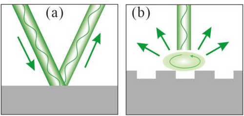
In 1960, Powell and Swan [39] demonstrated through electron energy loss experiments that the surface charge of metals can generate coherent resonance phenomena under incident light excitation and achieve enhanced electromagnetic fields on the material surface. Here, take the model of plane waves incident on the material surface as an example, as shown in the Figure 1.
Achieving localized optical field enhancement through the design of artificial microstructures is a challenge. Light is incident on a flat metal surface, where it undergoes reflection or absorption without any significant special effects. Light interacts with artificially structured metal surfaces, where the microstructures modulate the light, exciting surface plasmon resonance (SPR) or other optical resonance phenomena. This resonance enhances the localized electromagnetic field, resulting in higher absorption or scattering efficiency at specific wavelengths and exhibiting unique optical properties.
As shown in Figure 1, the upper part of the model is a uniformly transparent semi-infinite air medium, while the lower part is a semi-infinite uniform metal medium. It is assumed that a plane wave is irradiated from the top onto the surface of the metal medium. For planer surface (Figure 1a), incident light can only be reflected once, resulting in only little pressure. When the incident wave is irradiated onto a metallic nanostructure medium (Figure 1b), the lateral movement of electrons on the surface of the medium is hindered, which leads to the formation of a gradient distribution of electron concentration on the surface of the metallic medium, and thus the formation of charge oscillations confined to the surface of the medium.
The right side of the equation consists of two parts: one is determined by the cross product of the magnetic field and polarization called the scattering component, and its direction is consistent with the direction of the wave vector. The other part is calculated by gradient operators and electric fields named the gradient component, which is directed towards the gradient direction of the electromagnetic field in space. Assuming that the incident light propagates along the z-axis in a three-dimensional orthogonal Cartesian coordinate system (x, y, z axis), the polarization direction of its electric vector is the x-axis, and the corresponding angular frequency is ω. Substituting it into the expression for monochromatic time-harmonic electromagnetic waves and taking the time average, the time average expression for the density of optical pressure force per unit volume of dielectric material can be obtained:
3 Simulation Experiments and Analysis
3.1 Nanostructure Model
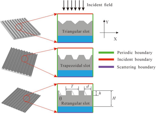
In order to facilitate calculation and improve accuracy, three array unit models were established. In the simulation, a linear-polarized TEM-mode electromagnetic wave enters from the upper boundary of the model shown in Figure 2 and propagates vertically downwards (Y-axis in Figure 2), with the polarization direction being horizontal (X-axis in Figure 2). The left and right boundaries of the model are periodic boundaries. The lower boundary is a scattering boundary. The nanostructure surface is composed of two layers, including the dielectric substrate layer (blue) and the metallic nanostructure layer (gray). The substrate layer serves as a hard substrate, and its thickness does not affect the simulation results in this study. The nanostructure layer consists of aluminum, and by designing specific geometry and morphology, strong resonance can be excited under external fields.
In the simulation, the incident light is a uniform flat top linearlypolarized pulsed laser with a wavelength of 527 nm, a spot radius of 10 mm, a pulse repetition rate of 3 kHz, a pulse width of 100 ns, and a total power of 20 W. The relative dielectric constant ε of the aluminum nanostructure layer is −25.24 + 5.42i [42] for incident wavelength of 527 nm, which is also needed for calculating optical pressure.
The structural parameters play a critical role in designing nanostructures for localized field enhancement. These parameters include key geometric factors such as shape, periodicity, depth, and other dimensional features. The shape of the nanostructure determines how light interacts with its surface, influencing phenomena like scattering and resonance. Precise control and optimization of these parameters is essential to achieve the desired field enhancement and tailor the optical properties of the nanostructures for specific applications.
Here, three typical geometric shapes are selected for comparison, including triangle, isosceles trapezoid, and rectangle, with similar widths and heights to ensure comparability. The model is defined by geometric parameters including the periodic parameter T (nm) of the array structure, the thickness H (nm) of the metal nanostructure layer, the characteristic depth h (nm) of the nanostructure, and the width d (nm). In addition, simulations have shown that the inclination angle of the slot side can affect the resultant horizontal force, so a certain inclination angle θ is set on the side of the rectangular nanostructure (see Figure 2) to study the optical pressure in the horizontal direction.
3.2 Comparison of Nanostructure's Form
First, the influence of nanostructures' form on resonant optical pressure is compared. The thickness H of the rectangular nanostructure in the simulation is 200 nm, the depth h is 60 nm, the width d is 200 nm, and the period T is 400 nm. The triangular nanostructure is an isosceles triangle with a height of 60 nm, and its width and period are consistent with the rectangular structure. The trapezoidal nanostructure is an isosceles trapezoid with a side inclination angle of 45°, and the other parameters are the same as those of the rectangular nanostructure. Figure 3 shows the surface electromagnetic field simulation diagrams of three nanostructures.
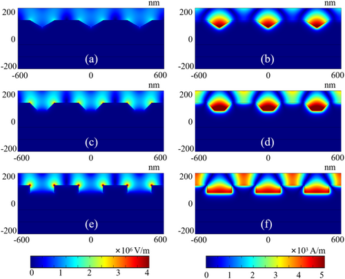
Figure 3a,c,e show the electric field distribution on the nanostructure surface with triangular, trapezoidal, and rectangular slots, respectively. Figure 3b,d,f show the corresponding magnetic field distribution. From the simulation results of the electromagnetic field, it can be seen that the nanostructure surface can generate local electromagnetic field enhancement. This is because the geometric parameters of the nanostructure are close to the wavelength of the incident light, which can meet the resonance conditions. In addition, among the three resonance modes, rectangular nanostructures can achieve more significant resonance and excite stronger local fields.
Finite element electromagnetic simulation is a direct and powerful method for visualizing and analyzing localized field enhancement. It provides a detailed insight into how light interacts with nanostructures of varying geometries, showcasing the spatial distribution and intensity of the optical field at subwavelength scales. Through finite element simulations, the interplay between geometry and localized optical response is clearly illustrated, enabling precise design and optimization of nanostructures for specific photonic and plasmonic applications.
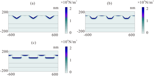
Finite element simulation serves as an essential tool to study how localized optical fields affect light-induced pressure density distribution, providing a detailed visualization of the interaction between electromagnetic fields and nanostructures. By simulating the optical pressure density in various geometries—such as triangular, trapezoidal, and rectangular nanostructures—key insights can be gained into how structural design influences optical forces.
Figure 4 shows that optical pressure is mainly generated in the depth range of several nanometers on the surface of the nanostructure. For comparison, suppose there is a planar mirror with a reflectivity of up to 100%, which is irradiated by the same incident light. The optical pressure on the reflective surface can be calculated using P = Spower (1 + r)/c, where Spower is the power of light irradiated onto the surface per unit area, r is the reflectivity of the mirror, and c is the speed of light (here is 3 × 10⁸ m/s). The simulation also took into consideration gold and copper as materials for comparison, and the surface optical pressures are calculated, as shown in Table 1.
According to Table 1, there is a correlation between optical pressure and the surface's form. The rectangular nanostructures can generate optical pressures of up to 4.85 N/m2, which is higher than that of trangular or trapezoidal nanostructures. On the other hand, the optical pressure on a planar mirror is only 1.41 N/m2, which is much smaller than any other nanostructure. This indicates that nanostructure can obtain higher optical pressure through resonance than that obtained by the planar mirror based on optical momentum exchange. It can also be found that different materials exhibit different optical properties under the same wavelength and structural conditions, and aluminum material could have greater force in our structure. It should be noted that the enhancement of optical pressure conforms to the law of momentum conservation, and its principle lies in the introduction of nanostructures that achieve resonance of surface electromagnetic fields, thereby enhancing optical pressure. For ease of understanding, it can also be compared to a pendulum, which can maintain enormous momentum and kinetic/potential energy under external periodic driving forces.
3.3 Influence of Nanostructures Width on Optical Pressure
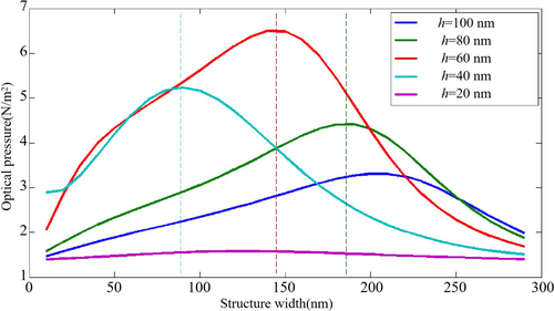
In order to further analyze the relationship between the geometric parameters of nanostructures and resonant optical pressure, the influence of nanostructure width on optical pressure was studied based on rectangular nanostructures that can generate strong resonant optical pressure The depth h of the nanostructure was 60 nm, the period T was 400 nm, and the variable was width d. A quantitative study was conducted on the influence of width variation on resonant optical pressure for five specific depths of nanostructures.
As shown in Figure 5, the five curves correspond to the variation of optical pressure with the width at depths of 20, 40, 60, 80, and 100 nm, respectively. The horizontal axis corresponds to the width d of the rectangular slot, and the vertical axis corresponds to the surface optical pressure. It can be seen that the resonant optical pressure is significantly affected by changes in width.
The relationship between resonance-induced optical pressure and the width of nanostructures is a critical factor in designing and optimizing nanostructures for photonic applications. The width of a nanostructure directly influences its optical resonance characteristics, including the intensity and spatial distribution of the optical field, which in turn affects the optical pressure generated during resonance excitation.
Taking the red curve for example (h = 60 nm), when the width of the nanostructure increases, the magnitude of the optical pressure gradually increases to its maximum value, reaching 6.5 N/m2 near the width of 140 nm. However, when the width further increases from 140 to 300 nm, the optical pressure gradually decreases. The other curves also exhibit a similar trend of increasing and then decreasing optical pressure influenced by width. The highest point for different curves is marked with a dashed line. It can be seen that the required width for generating the maximum optical pressure for rectangular slots with different depths is different. For rectangular slots with a depth of 40 nm, the maximum optical pressure corresponds to a width of 90 nm, while for rectangular slots with a depth of 80 nm, the maximum optical pressure corresponds to a width close to 190 nm. The above simulation shows that for a specific nanostructure depth, there will be an “optimal width” that can generate the strongest resonance and maximum optical pressure.
3.4 Influence of Nanostructure Depth
Next, the relationship between the nanostructure's depth and optical pressure was investigated. The width d of the nanostructure is 160 nm, the average period T is 400 nm, and the variable is depth h.
The relationship between resonance-induced optical pressure and the depth of nanostructures is a key factor in determining how effectively the structure can enhance and manipulate localized optical fields. The depth, often corresponding to the height of the nanostructure or the etching depth in a substrate, plays a significant role in defining the optical resonance conditions, field confinement, and resulting optical pressure distribution.
Figure 6 shows the influence of nanostructures depth on optical pressure. The horizontal axis corresponds to depth h of the rectangular slot, and the five curves correspond to nanostructures with widths of 160–240 nm. Taking the blue curve (d = 160 nm) as an example, when the depth increases, the resonant optical pressure increases first and then decreases. When the depth is around 55 nm (corresponding to Figure 7c,d), the optical pressure reaches a maximum value of about 6.8 N/m2, which is four times the optical pressure on the planar mirror in Figure 1. In addition, when the depth h decreases to around 0 so that the slot cavity resembles a planar mirror, the calculated optical pressure is close to 1.41 N/m2, which is also close to that of the planar mirror, confirming the reliability of the model.
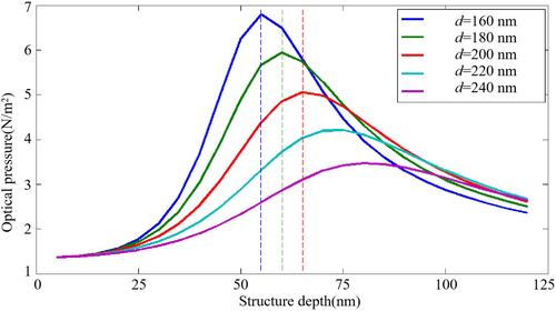
Compared with the width scan results in Figure 5, the depth scan results in Figure 6 also indicate that for a determined nanostructure width d, there is a unique “optimal depth” corresponding to the strongest resonance and maximum resonant optical pressure.
3.5 Side Inclination Angle for Optical Pressure Control
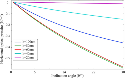
The previous simulation shows that the nanostructure surface can achieve enhancement and regulation of optical pressure in the optical axis direction. In the perpendicular direction, horizontal force could be obtained by changing the inclination angle of the nanostructure's slot. In the simulation, the inclination angle θ of the left side of the slot is gradually changed from 0° to 30°, and the variation of the horizontal force is shown in the Figure 7.
The relationship between resonance-induced optical pressure and the tilt angle of nanostructures (or the inclination of their sidewalls) is an important consideration in the design of nanophotonic systems. The tilt angle, which refers to the deviation of the sidewalls from being vertical, significantly influences the interaction between light and the nanostructure, thereby affecting the optical field distribution, resonance characteristics, and the resulting optical pressure. Steeper angles (near-vertical) tend to produce sharper resonances by confining light within narrower regions, enhancing field localization and generating higher peak optical pressures. This occurs because vertical sidewalls facilitate stronger coupling with incident light and more pronounced field enhancement at the edges.
As shown in Figure 7, the horizontal axis represents the inclination angle θ of the slot, and the vertical axis represents the horizontal force. The five curves correspond to nanostructures with a width of 200 nm and a depth ranging from 20 to 100 nm. The negative force indicates that the direction of the force is to the left. When the inclination angle is 0°, the nanostructure is a rectangular slot, and no horizontal force could be derived. When the inclination angle increases, the horizontal optical pressure also increases, and the relationship between horizontal optical pressure and inclination angle is approximately linear. Among the five curves, the red (h = 60 nm) and green (h = 80 nm) curves can reach a maximum horizontal force of 0.58 N/m2 with an inclination angle of 30°.
3.6 Influence of Incident Light Wavelength on Light Pressure
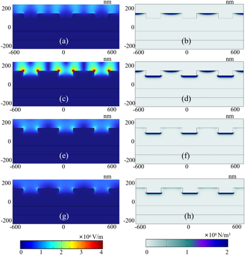
The previous sections reveal that certain geometry can affect the local electromagnetic field and thus enable enhancement and regulation of resonant optical pressure. However, whether this structure can resonate with incident light of different wavelengths is not yet determined. The following study is based on the nanostructures that can produce strong resonant optical pressure under incident light of 527 nm. The geometric parameters are at 160 nm, and the depth is 55 nm. The optical pressure under the incident wavelength of 427–927 nm (with 100 nm interval) is compared. The relative dielectric constant [40] under different wavelengths is shown in Table 2. Figure 8 shows the simulation results of the local electric field and force density under different wavelengths. According to the simulations, nanostructures that can generate strong resonance under 527 nm incident light do not show significant enhancement of the surface electromagnetic field under other wavelengths. In addition, force density simulations show that the force distribution concentrates at the convex of the nanostructure under incident light of 427 nm, while it concentrates at the concave of the nanostructure under incident light of 627 and 727 nm. Only under the incident light of 527 nm, there will be significant force distribution at both the convex and concave parts.
| 427 nm | 527 nm | 627 nm | 727 nm | 827 nm | 927 nm | |
|---|---|---|---|---|---|---|
| Relative dielectric constant | −16.43 + 2.87i | −25.24 + 5.42i | −35.45 + 9.90i | −44.81 + 18.32i | −43.51 + 25.87i | −49.23 + 17.15i |
|
Optical pressure (N/m2) |
1.97 | 6.79 | 2.55 | 2.28 | 1.44 | 1.43 |
The wavelength of the incident light plays a crucial role in determining the localized field distribution and the optical pressure distribution within nanostructures. As light interacts with nanostructures, different wavelengths of light can excite various resonance modes, leading to distinct field enhancements and optical pressures. The interaction between the incident light's wavelength and the geometric features of the nanostructure is key to understanding.
Table 2 shows more explicitly that the optical pressure under incident light of 527 nm is significantly stronger than the others. The reason is that the geometric parameters of nanostructures need to be designed to match the wavelength of the incident light in order to achieve the strongest resonance. For our designed nanostructures that can achieve strong resonance at 527 nm, their geometry does not hold strong resonance under other wavelengths. When the incident light wavelength exceeds 827 nm, the enhancement of optical pressure on the nanostructure is no longer significant, and the simulation results are similar to those of a planar mirror (in Table 1). This indicates that the incident light wavelength should not exceed the characteristic parameters of the nanostructure too much; otherwise, the structure will become ineffective.
4 Conclusion
In conclusion, we have demonstrated a method for regulating optical pressure based on nanostructures. When the wavelength of incident light matches the geometric parameters of the nanostructure, localized field resonance and maximum optical pressure can be achieved. A key design principle for nanostructures has been established based on extensive simulations. The results show that rectangular nanostructures outperform triangular and trapezoidal ones in terms of resonance effects, generating significantly higher optical pressure. By adjusting the depth and width of rectangular nanostructures, optical pressure can be effectively enhanced and modulated. Additionally, altering the inclination angle of the grooves enables the generation of horizontal optical pressure. The proposed architecture and methodology are versatile and can be extended to longer wavelengths and other material systems. In addition, future work can consider the regulation of optical pressure from multiple aspects, such as coherent light, polarization characteristics of the incident light, and quantum effects, which can offer the potential for broader applications in various optical and engineering fields. Our work lays a theoretical foundation for the development of optical pressure-sensitive components and supports the practical application of nanostructured mirrors in precision laser power measurement, non-destructive testing, and optical propulsion systems.
Author Contributions
Yukun Yuan: investigation, conceptualization, methodology, validation, visualization, writing – review and editing, writing – original draft, formal analysis, data curation, supervision. Qiang Zhang: investigation, methodology, validation, writing – original draft, formal analysis. Chunyang Gu: investigation, validation, visualization, formal analysis, writing – original draft. Siyu Huang: investigation, validation, formal analysis, writing – original draft. Fengzhou Fang: investigation, validation, formal analysis, writing – original draft.
Conflicts of Interest
The authors declare no conflicts of interest.
Open Research
Data Availability Statement
The data that support the findings of this study are available from the corresponding author upon reasonable request.


