Bias-Free Solar-to-Hydrogen Conversion in a BiVO4/PM6:Y6 Compact Tandem with Optically Balanced Light Absorption
Abstract
The high voltage required to overcome the thermodynamic threshold and the complicated kinetics of the water splitting reaction limit the efficiency of single semiconductor-based photoelectrochemistry. A semiconductor/solar cell tandem structure has been theoretically demonstrated as a viable path to achieve an efficient direct transformation of sunlight into chemical energy. However, compact designs exhibiting the indispensable optimally balanced light absorption have not been demonstrated. In the current work, we design and implement a compact tandem providing the complementary absorption of a highly transparent BiVO4 photoanode and a PM6:Y6 solar cell. Such bandgap combination approaches the optimal to reach the solar-to-hydrogen (STH) conversion upper limit for tandem photoelectrochemical cells (PECs). We demonstrate that, by using a photonic multilayer structure to adequately balance sunlight absorption among both tandem materials, a 25% increase in the bias-free STH conversion can be achieved, setting a clear path to take compact tandem PECs to the theoretical limit performance.
1 Introduction
In an attempt to mimic nature's photosynthesis process where sunlight energy is converted into chemical energy, numerous research efforts have been guided towards the development of semiconductor-based visible-light-driven water splitting systems.[1-5] However, reaching a high voltage combined with a broadband light absorption is a rather difficult hurdle to overcome for such systems, given that high and low band gap semiconductors are simultaneously needed. In addition, an effective sunlight absorption and charge separation, which typically require homogenous dense materials, must be combined with a strong catalytic activity, which demands a highly porous morphology to increase the specific surface of the water-semiconductor interface. An approach to make such combination viable is based on tandem structures where a high bandgap semiconductor is used as the photoanode of a photoelectrochemical cell (PEC), while the extra voltage needed to effectively split water is provided by a photovoltaic cell.[6-10] Relatively high solar-to-hydrogen (STH) conversion efficiencies have been achieved in systems where a nano-structuration to enhance light absorption in bismuth vanadate (BVO) based photoanodes was assisted with different kinds of solar cells.[11-13] In such systems, however, the high light scattering losses in the BVO, mostly caused by the nano-structuration, prevent the implementation of the ideal compact cell structure. Alternative approaches that have considered a compact pile up of the photoanode and a perovskite solar cell[14, 15] suffer from the need to have a highly transparent photoanode that reduces light absorption, setting a low limit for the maximum achievable STH conversion. In addition, the photoanode and the perovskite cell combinations tested exhibited a bandgap combination far from the ideal one. To reach the maximum STH conversion efficiency, which is estimated to be around 20% when realistic losses are taken into account, the optimal configuration should combine light absorbing elements based on ~1.9 and ~1.3 eV bandgap semiconductors.[16-19]
To overcome many of such limitations and obtain a compact tandem device where a high efficiency bias-free STH conversion or CO2 reduction can be eventually achieved, we proposed the design and implemented a compact tandem formed by piling up a highly transparent BVO based photoanode with a PM6:Y6 based organic photovoltaic (OPV) cell that exhibits a 1.3 eV bandgap, the optimal one to achieve the limit STH conversion efficiency for tandem-based PECs. A large portion of the novelty of the current work resides in introducing in between the two sides of the tandem a multilayer (ML) structure, alternating low and high index of refraction materials, to enhance light absorption in the thin BVO. In addition, such ML can properly balance sunlight absorption among both sides of the tandem, according to their respective light absorption profiles, to achieve an optimal sunlight absorption and transformation.
2 Results and Discussion
2.1 Modeling Multilayer Structures for an Optimal BVO-OPV Tandem Device Performance
To enhance the limited current density that can be obtained from the BVO layer, provided its small thickness and high bandgap, we consider a tandem configuration with an OPV cell incorporating a thin Ag layer, instead of the conventional ITO, as the electrode facing the BVO based photoanode. The reflectivity from such Ag electrode combined with a dielectric multilayer structure placed in between the photoanode and a PM6:Y6 OPV cell (see Figure 1a) can provide the adequate light distribution among both devices in the tandem according to their respective light absorption profiles, shown in Figure 1b. The optimal ML + OPV(Ag) configuration, in terms of number of layers, material combinations and thicknesses for such layers, can be determined using an inverse design approach targeting a maximum bias-free current density flowing through the tandem device. Provided the rather limited J-V performance of the BVO photoanode when compared to the OPV cell (c.f. Figure 1c) and to prevent operation of the tandem in the region where the J-V curve of the OPV bends, in this work we consider a computational model that combines the general transfer matrix formalism[20] for the computation of the short circuit current densities (JSC) of the photoanode and OPV cell, together with a diode approximation to describe the J-V characteristics of both tandem elements.[18, 21-24] To find the ML + OPV(Ag) configuration that leads to maximized bias-free current density, this model was combined with a genetic algorithm, set to optimize the operating point of the tandem device (see Figure 1c). A complete description of the model used, together with the experimental relationships found between the electrical parameters for both photoanode and OPV cell can be found in Section S1, Supporting Information.
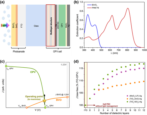
The refractive indexes of all the materials considered in the simulations are given in Section S2, Supporting Information. The SnO2 layer of the photoanode was not included in the computation, as it was found to have a negligible optical role, as illustrated in Figure S7, Supporting Information. To limit charge recombination and prevent large losses in charge collection in the OPV cell, its active layer was allowed to have a maximum thickness of 120 nm,[25] while to maintain a high conductivity for the front electrode of that same cell, the minimum thickness of the Ag was set to 7 nm.[26] The FTO and BVO layers in the photoanode were kept fixed to the experimentally determined thicknesses, of about 90 and 600 nm, respectively, as extracted from the cross-section SEM micrographs of Figure S8, Supporting Information. Among the different combinations of dielectric materials considered in the computation of the ML when applying the inverse design approach, we found that the highest bias-free current density would be achieved when using TiO2 and SiO2, provided they exhibited the highest index contrast. As can be seen in Figure 1d, the other two combinations we considered, MoO3-LiF and TiO2-ZnO, exhibited a lower performance. The optimal configurations for the ML + OPV(Ag) determined from the inverse design approach employed are presented in Table S1, Supporting Information, for TiO2-SiO2 ML structures with up to 8 dielectric layers. Note that, as seen in Figure 1d, the current density at bias-free conditions has a tendency to saturate as the number of layers in the ML increases, and only small gains are achieved beyond the 8-layer ML (ML8). When the ML + OPV(Ag) tandems are compared to a tandem incorporating an ITO based OPV cell OPV(ITO), the maximum predicted gain was close to 20%.
2.2 Light Absorption Distribution in the BVO and OPV Cell
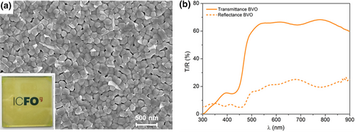
The fabrication of a compact tandem requires a high transparency for the photoanode in the region of the solar spectrum where the OPV absorbs light and the BVO does not. To achieve that, a compact 90 nm thick BVO film was deposited on top of a glass/FTO/SnO2 substrate. SEM micrographs from Figure 2a and Figure S8, Supporting Information of such BVO layer reveal a polycrystalline structure with small grain sizes ranging between 100 and 200 nm, which ensure a negligible light dispersion by scattering, as can be seen in the inset from Figure 2a. Indeed, as seen in Figure 2b, despite the excellent absorption observed in the low wavelength range, for the spectral region above 500 nm the photoanode transmittance observed was higher than 60%.
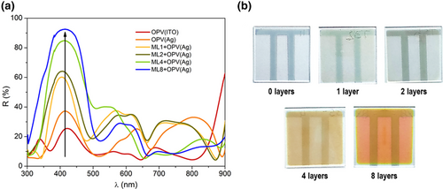
On the other side, the tandem was completed with the OPV(Ag) cell deposited on top of the ML structures. We fabricated PM6:Y6 solar cells on top of ML structures composed of 0, 1, 2, 4, and 8 layers in the ML with the configurations presented in Table S1, Supporting Information. To fabricate ML structures where the layer thickness would accurately match the ones estimated by the computational approach, we performed a pre-calibration of the layer thicknesses by measuring the transmittance and reflectance of single layers, for different deposition times. In all the five ML + OPV(Ag) structures fabricated, the electrode facing the glass substrate and the photoanode in the tandem was an Ag layer ranging from 7 to 14 nm, placed in between two 5 nm ZnO layers. The fabrication procedure and performance parameters of such electrode, as well as the role played by the two ZnO layers, can be found elsewhere.[26, 27] Despite the low thicknesses deposited, the sheet resistances of all silver electrodes were quite close to the one of the commercial ITO-covered substrates, as demonstrated in Figure S9, Supporting Information. This resulted in a very good performance for all the OPV cells, regardless of the ML and silver thickness used, as shown in Table S2, Supporting Information. As seen in Figure 3a, the experimentally measured reflectivities in the region where the BVO absorbs increase gradually, up to above 90%, when the number of layers in the ML increases. On the other hand, such reflectivities remain roughly in a 10–40% range in the spectral region where the OPV cell is expected to contribute, in good agreement with the numerical predictions shown in Figure S10, Supporting Information. The increase in reflectivity observed for lower wavelengths is achieved from constructive interference of the light inside the ML + OPV(Ag), which peaks slightly above 400 nm. The width of the wavelength range, spanning from about 300 to 500 nm, where this reflectivity is enhanced, is essentially determined by the index contrast between the two materials used in the ML. However, as seen in Table S1, Supporting Information, to combine this enhanced reflectivity for wavelengths within the BVO absorption band with an increased transmission of light for wavelengths within the PM6:Y6 absorption band, the inverse design approach found MLs that deviate from the periodic /4 configuration. In particular, the ML + OPV(Ag) sample fabricated with the 8-layer ML exhibits the optimal reflectance profile to reach the highest current density from the tandem. When inspecting the ML + Ag without the rest of the OPV cell structure, shown in Figure 3b, we clearly observe a color shift from a colorless ML, when only the Ag layer is deposited on bare glass, towards an orange color for the 8-layer ML.
2.3 Operation of the PEC under Different ML + Ag Structures
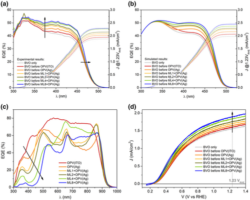
To investigate the role of the ML in enhancing the JSC (current density at 1.23 VRHE) extracted from the photoanode, which is what actually sets the limit performance for the bias-free PEC, while clearly separating the ML contribution to such JSC enhancement from the catalysis, a series of experiments in PECs incorporating the tandem with different MLs were performed using an electrolyte solution of 1.0 m KBi (pH 9) with 0.2 m of a hole scavenger. The experimentally measured and computed photoanode external quantum efficiencies (EQEs), shown in Figure 4a,b, respectively, are progressively enhanced in the mid to long wavelength side of the BVO absorption band and apparently infrared shifted, as the number of TiO2/SiO2 bilayers increases. The apparent IR shift of the EQE clearly indicates that the conversion of absorbed photons to collected holes has not reached its limits in BVO based PECs. On the contrary, there is a clear saturation of the EQE on the short wavelength side, even when the number of layers in the ML is small. This saturation, which results from a short exciton diffusion and low minority carrier mobility, extends to longer wavelengths when the number of layers in the ML approaches its maximum. This proves that the light absorption enhancement provided by the MLs is very effective in the shorter towards mid wavelength region of the BVO absorption band. Note that, when the high reflectivity MLs are used, it is the poor electrical performance of the photoanode that limits the overall JSC, not a deficient light absorption. The saturation in the light absorption enhancement is in agreement with the increase and subsequent saturation in the reflectivity of the ML + OPV(Ag) seen in Figure 3a when the number of layers in the ML approaches eight. Such an increase in the number of layers in the ML to improve light absorption in the BVO has also a clear side effect on the EQE of the OPV cells. For wavelengths above 450 nm, the EQE of the OPV cell exhibits a very slight reduction when the number of layers in the ML is increased, because the number of interfaces is also increased. But the relevant thing is that, for wavelengths below 450 nm, the EQE is reduced due to an enhanced reflectivity of the cell in this range, resulting from optical interference by the ML. For instance, for the ML8-based structure, the EQE of the OPV is practically zero in the spectral region ranging from 300 to 450 nm. In fact, for such ML8-based structure, the EQE of the photoanode exhibits minimal overlap with the EQE of the OPV, confirming an optimal distribution of the light absorption in terms of its wavelength. As seen in Figure 4c, when the number of layers in the ML is reduced, the EQE of the OPV expands towards the UV side of the spectrum. The improvement in the BVO light absorption with the number of layers in the ML is directly translated to a better performance of the photoanode, as demonstrated by the J-V responses of Figure 4d. A sequential enhancement in the JSC of the photoanode with the number of dielectric layers is demonstrated, in agreement with the current density enhancement obtained from the integration of the experimental EQE spectra shown in Figure 4a. For both cases, the percentual improvement in the photoanode JSC in comparison to the use of a standard OPV(ITO) solar cell was in good agreement with the computational predictions, as demonstrated in Table 1, reaching almost 19% for the ML8-based structure.
| Sample | Experimental JSC improvement from EQE [% of ITO-OPV] | Experimental JSC improvement from J-V [% of ITO-OPV] | Simulated JSC improvement [% of ITO-OPV] |
|---|---|---|---|
| OPV(ITO) | 100.0 | 100.0 | 100.0 |
| OPV(Ag) | 103.9 | 103.2 | 104.7 |
| ML1+ OPV(Ag) | 107.3 | 106.6 | 109.5 |
| ML2+ OPV(Ag) | 110.3 | 109.8 | 111.2 |
| ML4+ OPV(Ag) | 116.5 | 114.8 | 115.1 |
| ML8+ OPV(Ag) | 117.6 | 118.5 | 118.9 |
2.4 Bias-Free H2 Production with the BVO Photoanode/ML + Ag/PM6:Y6 OPV Tandem
To facilitate the oxygen evolution reaction at the electrolyte-BVO interface, a FeOOH/NiOOH catalyst was photo-electro-deposited on the exposed surface of the BVO photoanodes. As shown in Figure S11a, Supporting Information, the optical properties, and in particular the light transmission, of the photoanode are practically unaffected by the deposition of such catalyst. However, the oxygen evolution and hydrogen production in a pH 9 electrolyte solution of 1.0 m KBi are considerably improved when such catalysts are deposited on the BVO surface. As seen in Figure S11b, Supporting Information, the J-V response of the BVO with the addition of the catalyst is characterized by a decrease in hysteresis, by a downshift of the onset potential from 0.48 to 0.38 V, and by an increase in short circuit current density at 1.23 VRHE from 0.52 to 1.44 mA cm−2. This way, the J-V behavior gets closer to the one obtained with the incorporation of 0.2 m of a hole scavenger in the electrolyte solution, which is unaffected by the presence of the catalyst, as revealed in Figure S11b, Supporting Information.
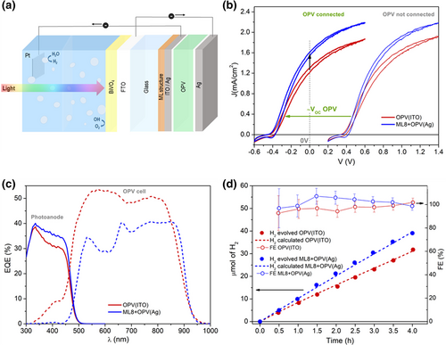
The tandem device was mounted at the back of the photoelectrochemical cell, where the photoanode was in contact with the electrolyte solution of 1.0 m KBi at pH 9 and illuminated from the front-side, while the OPV cell was placed outside, as shown as in Figure 5a and in Section S6, Supporting Information. The electrical response of the PEC was evaluated in a two-electrode configuration where the cathode used for the hydrogen evolution reaction was a Pt mesh. When measuring the hydrogen production, the photoanode, PV cell and cathode were connected in series, as shown schematically in Figure 5a. The J-V response of the PEC was evaluated by applying an external voltage to the PEC both in the case where the electrical circuit was closed by the OPV cell, as shown in Figure 5a, and when the OPV cell was electrically by-passed and its sole role was to provide light reflectivity, being the photoanode directly connected to the Pt mesh. As shown in Figure 5b, in the former case, corresponding to the OPV connected in series in between the photoanode and the cathode, the J-V curves were down shifted by 0.775 and 0.795 V, which approximately correspond to the open circuit voltages (VOC) of the OPV, relative to the ones where the OPV is not connected. Such shift was kept practically unaltered regardless of the photocurrent generated (cf. Figure S15, Supporting Information), which indicates that the solar cell is not limiting the performance of the tandem for any of the configurations studied. At 0 V of applied voltage we obtained a completely bias-free H2 production, resulting in a current density increase from 1.26 to 1.57 mA cm−2 for the photoanode/OPV(ITO) and for the photoanode/ML8 + OPV(Ag) tandem, respectively. Note that the photoanodes chosen for the experiments of Figure 5b had very similar J-V response, as demonstrated in Figure S16, Supporting Information. The small differences observed between the two curves in Figure S16, Supporting Information might have resulted in very slight changes in the shapes of the J-V responses reported in Figure 5b, but they did not significantly affect the current densities delivered by the tandem devices. In other words, it is the combination between the ML and OPV incorporating the transparent Ag the main responsible for the 25% higher bias-free current density experimentally observed. This confirms that a proper distribution of the light absorption among the two sides of the tandem is key in the implementation of an efficient bias-free STH conversion. A further confirmation of the relevance of such proper distribution of the light in terms of the wavelength to match the absorption bands of the different elements of the tandem is seen in the EQEs shown in Figure 5c, where the photoanode EQE is enhanced in a wavelength range spanning almost the entire absorption band of the BVO, while the EQE of the OPV is correspondingly reduced in the UV side but clearly less affected in the IR side of the absorption band. Given the high performing parameters of the PM6:Y6 OPV cell used, shown in Table S2, Supporting Information, the potential JSC obtainable from that cell still remains several times higher than the one provided by the photoanode. The experimental measurements of the hydrogen evolution, shown in Figure 5d, confirm an increase in gas production of about 25% when the ML8 light management structure is used. Indeed, the hydrogen evolution rate is seen to increase from 7.8 μmol (cm2h)−1, for the photoanode/OPV(ITO) tandem, to 9.9 μmol (cm2h)−1, for the photoanode/ML8 + OPV(Ag) device. This is in quite good agreement with the theoretically predicted rates when taking into account the bias-free current densities measured, and represented by the dashed lines in Figure 5d. The faradaic efficiencies (FE) determined for both tandems were very close to 100%, which corresponds to STH conversion efficiencies of 1.55% and 1.93% for the photoanode/OPV(ITO) and the photoanode/ML8 + OPV(Ag), respectively. Note that, at the beginning of the reaction the error in the measurement of the FE is a bit large, as seen by the error bars in Figure 5d, provided the volume readings for such small amounts of produced hydrogen were not extremely precise.
Long term operation studies, performed at bias-free conditions and shown in Section S8, Supporting Information, reveal a very similar behavior for both tandem assemblies, regardless of the electrode used for the OPV cell. As seen in Figure S17, Supporting Information, in the first couple of hours the photocurrent decreased quite fast until reaching nearly 60% of the initial value, after which it became stable for the remaining time of the study, with some oscillations attributed to the formation and release of bubbles. An analysis of the BVO and OPV performances made right before and after these stability measurements, shown in Figures S18 and S19, Supporting Information, revealed that the photoanode is quite stable under long term operation and does not undergo significant changes in morphology and photoelectrochemical performance during that time. In contrast, the OPV cell suffers a reduction in VOC and fill-factor when it is under continuous illumination, which ends up reducing the photocurrent of the tandem device at bias-free conditions. This drop in cell performance after 12 h of continuous irradiation was similar for both OPV(ITO) and ML8 + OPV(Ag) samples, as shown in Figure S18, Supporting Information, confirming that the use of the ML is not affecting the stability of the photovoltaic device. In addition, part of this performance can be recovered after storage for 1 day in dark and dry conditions, as illustrated in Figure S18, Supporting Information.
3 Conclusion
We have designed and demonstrated a path for combining low and high bandgap materials to eventually achieve the limit efficiency in the conversion from sunlight into chemical energy in compact tandem-based PECs. Light absorption in the tandem structure herein implemented is distributed and accurately balanced among the two absorption layers in the tandem according to their respective absorption bands. As the low bandgap element, we fabricated a PM6:Y6 based organic solar cell, which exhibits the optimal low bandgap and excellent optoelectronic parameters for achieving such STH limiting efficiency conversion in tandem-based PECs. As the high bandgap element, we implemented a photoanode based on a light dispersion free BVO thin layer. The high transparency and small thickness for the BVO layer is a hurdle that we demonstrated that can be bridged with the implementation of tailor-made light distribution dielectric structures. We have shown that the combined effect of a ML structure alternating low and high refractive index dielectric materials can lead to light absorption in BVO approaching its current limits, translated into a STH conversion that is enhanced by 25%. To further increase such STH conversion and reach the limit efficiencies predicted for the tandem-based PECs, future work should focus on increasing light to electron–hole pair generation in the BVO photoanode. A possible route would be the incorporation of a low light scattering highly ordered three-dimensional nano-structured photonic design to enhance light absorption below the direct bandgap, which would allow to further thinning down such BVO layer while enhancing its electronic properties.
4 Experimental Section
Materials
Bismuth(III) nitrate pentahydrate (Bi(NiO3)3·5H2O, 99.99%), vanadyl acetylacetonate (C10H14O5V, 97%), acetylacetone (C5H8O2, 99%), tin(II) chloride dihydrate (SnCl2·2H2O), iron(II) sulfate heptahydrate (FeSO4·7H2O, 99%), nickel(II) sulfate hexahydrate (NiSO4·6H2O, 98%), boric acid (H3BO3, 99.5%), potassium hydroxide (KOH, flakes, 90%), sodium sulfite (Na2SO3, 98%), zinc acetate dihydrate (Zn(CH3COO)2·2H2O), ethanolamine (NH2(CH2)2OH), 2-methoxyethanol (CH3O(CH2)2OH) and 1-chloronaphthalene (C10H7Cl) were all purchased from Sigma Aldrich. The polymers PM6 (Batch No. YY20260CH-2) and Y6 (Batch No. DW8095P) were both purchased from 1-Material. All chemicals were used as received, without any further purification.
MoO3 and Ag pellets, as well as 2-inch diameter Ti (99.995%), Si n-type (99.999%), ZnO (99.999%) and Ag (99.99%) sputtering targets were acquired from Kurt J. Lesker company. Eagle XG glass substrates were purchased from Coresix Precision Glass, FTO coated glass substrates (≈7 Ω sq−1) were bought from Sigma Aldrich, while patterned ITO glass substrates (≈13 Ω sq−1) were obtained from Lumtec.
Fabrication of the SnO2/BiVO4 photoanodes
SnO2 layers were deposited on FTO covered glass substrates, pre-cleaned consecutively with detergent solution (Helmanex), acetone, isopropanol and D.I. water, and treated with ozone in a UVO cleaner (Jelight model 42). To prepare the solution, the tin precursor was dissolved in isopropanol with a concentration of 30 mm, stirred for 5 h, and kept under ambient conditions for 24 h before use. It was then spin-coated (WS-650-lite series from Laurell Technologies) on the FTO substrate at 56 g-force for 30 s and annealed in a box furnace at 500 °C for 1 h.
BiVO4 films were spin-coated on SnO2/FTO following a procedure adapted from literature.[28] Two solutions of vanadyl acetylacetonate (0.03 m in acetylacetone) and of bismuth nitrate pentahydrate (0.2 m in acetylacetonate), were prepared separately and sonicated for 15 min. The BiVO4 precursor solution was obtained after mixing 20 mL of the vanadyl acetylacetonate solution with 3 mL of the bismuth nitrate solution, sonicating for 10 minutes and filtering with 0.45 μm pore PTFE filter membranes. For the deposition, 100 μL of the precursor solution were spin-coated twice in a row onto the substrate during 10 s at 14 g-force, with an acceleration rate of 250 rpm s−1, and then annealed for 10 min at 500 °C (RH = 30%) in a box furnace. Such deposition-annealing process was repeated 11 times. After the last spin-coating, the substrate was annealed at 500 °C for 2 h.
To prepare the photoanodes, the BiVO4 samples were cut into pieces of ~1.25 × 1.25 cm with a carbon nitride blade. A small section of the BiVO4 film was then etched using a cotton swab embedded in a 0.5 m solution of HCl, in order to expose the FTO, where the electric contact was created by soldering with indium a silver conductive tape (from 3M).
Deposition of FeOOH/NiOOH catalyst on the surface of the BiVO4
Two solutions of FeSO4 (0.1 m) and NiSO4 (0.1 m), were sequentially used to deposit the FeOOH/NiOOH catalyst on the surface of the BiVO4. Photo-assisted electrodeposition was performed under AM 1.5G illumination, in a 3-electrode configuration with the BiVO4 acting as working electrode, a platinum wire (CH instruments CHI115) as counter electrode and an Ag/AgCl electrode in 1 m KCl (CH instruments CHI111) as reference. For the photo-assisted electrodeposition of the FeOOH, a 0.25 VAg/AgCl potential was applied during 6 min, the first 5 under 1 sun illumination and the last one in dark. After that, the NiOOH was deposited at 0.11 VAg/AgCl during 5 min under 1 sun followed by 1 min in dark conditions.
Fabrication of the 1-dimensional light management structures
All the layers of the nanophotonic structures were deposited by magnetron sputtering (AJA International Inc) on pre-cleaned Eagle XG glass substrates. The sputtering chamber was initially pumped down to a base pressure of ≈10−6 mTorr, the distance between target and substrate was kept at 30 cm and the rotation speed of the holder was set to 60 rpm. All materials were deposited at room temperature. The Ag and ZnO layers were sputtered in a pure Ar atmosphere, from Ag and ZnO targets, at a working pressure of 3 mTorr. For Ag, a DC power of 18 W was applied, while an RF power of 60 W was used for the ZnO deposition. TiO2 was reactively sputtered from a Ti target in a mixture of Ar/O2 with flux ratio of 10:2.2, using a DC power of 250 W and a working pressure of 2 mTorr. Finally, SiO2 was sputtered from an n-type Si target with an RF power of 120 W, in an atmosphere containing Ar/O2 with flux ratio of 10:1.1 at 3 mTorr pressure.
Fabrication of the OPV solar cells
PM6:Y6 organic photovoltaic cells were prepared in a similar way as described in the literature.[29] A precursor solution of sol–gel ZnO (0.15 m) was prepared by dissolving zinc acetate (99 mg) dihydrate and ethanolamine (27 mg) in 2-methoxyethanol (3 mL). Such solution was stirred in air for 2 h at 60 °C followed by 12 h at room temperature. It was then spin-coated on top of the patterned ITO substrates or the nanophotonic structures described in previous section at 350 g-force during 30 s, and annealed in air at 150°C for 30 min, in order to form a ~20 nm thick electron transporting layer. For the solar cell active layer, PM6:Y6 (1.0:1.2 weight ratio) was dissolved in chloroform to obtain a precursor solution with a total concentration of 16 mg mL−1. Such solution was left stirring overnight at room temperature in a N2-filled glovebox, and a 1-chloronaphthalene additive (0.5% volume) was added 40 min prior to spin-coating. The speed rate was adjusted to 126 g-force in order to obtain a layer thickness of ~110 nm, as optimized by the computational simulations described in Sections S1 and S2.1, Supporting Information and shown in Table S1, Supporting Information. A 5 nm thick MoO3 hole transporting layer was then thermally evaporated at a rate of 0.6 Å s−1, followed by a nominal 100 nm Ag layer to form the cell contacts, also deposited by thermal evaporation at a rate of 1 Å s−1 and at a base pressure <5 × 10⁻⁶ mbar. The area of the fabricated photovoltaic cells was 0.06 cm2, defined by the overlap between the bottom ITO/nanophotonic structures and the top silver electrodes. For the electrochemical measurements, the devices were encapsulated with glass and sealed with an UV curable adhesive (Norland Optical Adhesive 73), cured for 1.5 min, before testing. The electric connections were created by using Ag conductive tape connected with silver paste to the evaporated Ag contacts of the OPV cell.
Assembly of the monolithic tandem device
The tandem devices were assembled as shown in Figure S12, Supporting Information, by placing the OPV cells on the back side of the BiVO4 electrodes, using an UV curable index-matching resin to fix the two glasses together. An external wire was used to electrically connect the BVO photoanode to the cathode of the OPV cell, while the anode of the photovoltaic cell was used as a working electrode for the tandem configuration.
Photovoltaic measurements
The J-V curves of the OPV cells were measured under 1-sun illumination, from an ABET Sol3A 1000 W m−2 solar simulator, with a Keithley 2400 sourcemeter. The intensity of the light source, a 300 W xenon lamp from Ushio, was previously calibrated with a Hamamatsu silicon photodiode (with a KG-5 filter, area 0.1296 cm2) certificated by ISE Fraunhofer. External quantum efficiencies were measured at 130 Hz, by means of a QEX10 system from PV Measurements Inc., and using as reference the spectral response of a calibrated silicon cell.
Photoelectrochemical measurements
J-V and EQE measurements were performed using a custom-made photoelectrochemical cell with a single compartment, designed at ICFO institute and illustrated in Figures S13b and S14, Supporting information. A solution of potassium borate buffer (KBi, 1.0 m) with pH 9 was chosen as supporting electrolyte, and it was prepared by dissolving boric acid (62 g) in mili Q water (1 L), later adding KOH to adjust the pH to the desired value. When in the absence of the FeOOH/NiOOH catalysts in the BiVO4 surface, Na2SO3 (0.2 m) was added to the KBi buffer as a sacrificial hole acceptor. To measure the bare BiVO4 (both alone and in front of a non-patterned OPV cell), a 0.5 cm2 circular window was used. On the other hand, for the tandem devices the active area was limited by the photovoltaic cell to 0.06 cm2, which was obtained by the use of a black vinyl sticker, as shown in Figure S12, Supporting Information. Optical microscopy was used to confirm the positioning of this mask.
For the J-V measurements, an Abet Sun 2000 solar simulator, incorporating a 550 W xenon lamp from Ushio, was used to simulate 1-sun solar light AM 1.5G illumination, and its intensity was calibrated with a silicon photodiode prior to each measurement. Bias voltages were applied by a Biologic SP-300 potentiostat, and scanned at a rate of 50 mV s−1. For the BiVO4 photoanodes, the measurements were performed in a 3-electrode configuration, with a platinum wire (CH instruments CHI115) serving as counter electrode and an Ag/AgCl electrode in 1 m KCl (CH instruments CHI111) acting as reference. For the tandem devices, both 3- and 2-electrode measurements were performed: in the last case, the platinum wire served simultaneously as counter and reference electrode.
EQE measurements were carried out in a setup equipped with an Oriel 260 Cornerstone monochromator, from Newport Instruments, illuminated with a 300 W xenon lamp. For increased precision in the values obtained, long pass filters were installed in an automated wheel, to cut out more energetic second-harmonic photons from the grating. The monochromatic power intensity was recorded with a calibrated S120VC silicon photodiode, from Thorlabs. A Biologic SP-300 potentiostat was used to apply a fixed voltage, in a 3-electrode configuration, and to record the photocurrent density for each individual wavelength.
Additional characterization
Optical transmittance and reflectance measurements were carried out with a Perkin-Elmer 950 UV/Vis spectrometer. Surface and cross-section micrographs were obtained by scanning electron microscopy with a Zeiss series Auriga FIB-SEM microscope, operated at 5 kV. Topography micrographs of the films were acquired by a Park Systems NX10 atomic force microscope in non-contact mode, with a NCHR silicon tip. The sheet resistance of the OPV electrodes was determined by a 4-point probe method with a cascade Microtech C4S-44/7S probe head connected to a Keithley 2110 multimeter.
Acknowledgements
The authors also acknowledge the financial support by the European Commission through the LICROX project (grant 951843). In addition, the work was partially funded by Ministerio de Ciencia e Innovación (grants Nos. CEX2019-000910-S and PID2020-112650RB-I00), Fundació Cellex, Fundació Mir-Puig, and Generalitat de Catalunya through Centres de Recerca de Catalunya. F.B.T acknowledges the financial support by the Agencia Estatal de Investigación (grant PRE2018-084881). C.R. acknowledges support from the Ministerio de Ciencia e Innovación/Agencia Estatal de Investigación (grant FJC2020-043223-I) and the Severo Ochoa Excellence Post-doctoral Fellowship (grant CEX2019-000910-S).
Conflict of Interest
The authors declare no conflict of interest.


