High-Quality and Wafer-Scale Cubic Silicon Carbide Single Crystals
Abstract
Cubic silicon carbide (3C-SiC) has superior mobility and thermal conduction over that of widely applied hexagonal 4H-SiC. Moreover, much lower concentration of interfacial traps between insulating oxide gate and 3C-SiC helps fabricate reliable and long-life devices like metal-oxide-semiconductor field effect transistors. However, the growth of high-quality and wafer-scale 3C-SiC crystals has remained a big challenge up to now despite decades-long efforts by researchers because of its easy transformation into other polytypes during growth, limiting the development of 3C-SiC-based devices. Herein, we report that 3C-SiC can be made thermodynamically favored from nucleation to growth on a 4H-SiC substrate by top-seeded solution growth technique, beyond what is expected by classical nucleation theory. This enables the steady growth of high-quality and large-size 3C-SiC crystals (2–4-inch in diameter and 4.0–10.0 mm in thickness) sustainable. The as-grown 3C-SiC crystals are free of other polytypes and have high-crystalline quality. Our findings broaden the mechanism of hetero-seed crystal growth and provide a feasible route to mass production of 3C-SiC crystals, offering new opportunities to develop power electronic devices potentially with better performances than those based on 4H-SiC.
1 Introduction
Silicon carbide (SiC) is an important semiconductor material for fabricating power electronic devices that exhibit higher switch frequency, lower energy loss, and substantial reduction both in size and weight in comparison with its silicon (Si)-based counterparts.[1-4] Currently, most devices, such as metal-oxide-semiconductor field effect transistors (MOSFETs), which are core devices used in electric vehicles, photovoltaic industry and other applications, are fabricated on a hexagonal polytype 4H-SiC because of its commercial availability.[5, 6] Cubic silicon carbide (3C-SiC), the only cubic polytype, has a moderate band gap of 2.36 eV at room-temperature, but a superior mobility and thermal conduction than that of 4H-SiC.[4, 7-12] Moreover, the much lower concentration of interfacial traps between insulating oxide gate and 3C-SiC helps fabricate reliable and long-life devices.[8-11, 13-15] The growth of 3C-SiC crystals, however, has remained a big challenge up to now despite of decades-long efforts by researchers because of its easy transformation into other polytypes during growth,[16-20] limiting the development of 3C-SiC-based devices.
The physical-vapor-transport (PVT) method is the state-of-the-art technique for growing hexagonal 4H- and 6H-SiC crystals. This involves heating raw SiC powder above 2000 °C to produce gas species containing Si and carbon (C), which are then transported to a cold end where crystallization occurs on a seed crystal.[21, 22] This process, however, does not work well when it comes to grow 3C-SiC as a higher Si/C ratio in gas species is required. A modified method, close-space PVT, by which a high enough Si/C ratio can be created by separation of raw SiC powder and seed 1–2 mm, allows to grow 3C-SiC.[23, 24] This is not a practical pathway to mass production considering the very limited thickness (<2 mm). Recently, a reduction in defects for 3C-crystals can be achieved by further PVT process on a free-standing single crystal first prepared by chemical vapor deposition on Si substrates.[25] But the grown SiC boules' thickness and the efficiency are still problematic toward mass production of wafers although in-situ switch between the two involved growth methods is feasible.[26] In addition, early attempts to grow 3C-SiC from high-temperature melts are not successful either on 6H- or 4H-SiC seeds because these two polytype inclusions always coexist along the grown 3C-SiC.[19] Alternatively, 3C-SiC films are directly deposited on Si substrate then further process into devices on it. But the large lattice mismatch (~19%) and thermal expansion mismatch (~8%) between 3C-SiC and Si result in too high density of defects, significantly deteriorating the performances of devices.[8] Thus, available technique is highly desired to production of high-quality and wafer-scale 3C-SiC single crystals.
Structurally, 3C-SiC differs from 4H-SiC in the stacking of identical Si-C bilayers.[27] In 3C-SiC, the bilayers are stacked as a crystallographic plane (111) in the sequence of ABC.[27] In contrast, in 4H-SiC, the bilayers are stacked as a (0001) plane in the sequence of ABCB.[27] The two stacking ways do not cause a significant difference in formation energy, typically a few meV per formula higher for 3C-SiC than for 4H-SiC at 0 K.[27] At temperatures around 1727 °C, the energy difference between 3C-SiC and 4H-SiC widens to about 5–10 meV per formula, enhancing the stability of 4H-SiC further. However, it is not clear why 3C-SiC is often found as inclusions in 4H-SiC films deposited at around 1650 °C. Ramakers et al.[28] proposed that surface energy plays a crucial role in stabilizing 3C-SiC over 4H-SiC and 6H-SiC, as the former has surface energy that is 20–150 meV per SiC lower than the latter two. This also means that the 3C polytype may be energetically favored over a certain temperature range if surface energy contributes significantly to the change in the overall formation energy, which depends on different surface reconstruction configurations.
In this study, we smartly modified the surface tension of the melt via nitrogen (N) incorporation for the growth of 3C-SiC via TSSG, effectively adjusting the solid–liquid interfacial energy of SiC and melt. By decreasing the solid–liquid interfacial energy of 3C-SiC/melt and increasing that of 4H-SiC/melt, the nucleation and growth of 3C-SiC is more energetically favorable than that of 4H-SiC on a 4H-SiC substrate. In this way, high-quality and wafer-scale 3C-SiC single crystals (2–4-inch in diameter and 4.0–10.0 mm in thickness) are successfully grown via TSSG. Our study provides a feasible route to mass production of 3C-SiC crystals and facilitates the development of new power electronic devices potentially with better performances that are widely used in electric vehicles and photovoltaic industry.
2 Results and Discussion
2.1 Considerations on Stabilizing and Growth of 3C- over 4H-SiC
We start off our exploration of growing 3C-SiC single crystals by employing the TSSG technique. Our strategy is based on two primary considerations. First, the interfacial energy between SiC and melts can be more easily adjusted through altering their chemical compositions in TSSG in comparison to PVT, in which only the interface between SiC and gaseous phase exists. Liquid phases are generally thought to be has a more significant effect in changing the interfacial energy than gaseous phases do.[29] It is possible to achieve a lower enough interfacial energy for 3C- over 4H-SiC, which will prioritize the nucleation and subsequent growth for former, and suppress that for the latter. Second, 4H-SiC crystals larger than 4-inch have been successfully obtained by TSSG at 1700–1800 °C.[30] In this study, we demonstrate that our strategy works well and bulky 3C-SiC crystals up to 4-inch in diameter and more than 4.0 mm in thickness are successfully grown.
Figure 1a shows the schematic setup for growing 3C-SiC by TSSG. Crucibles made from high-purity graphite serve as both container and carbon source. Inside the crucible, a melt temperature gradient is set as 5–15 °C cm−1 with a temperature of top melt at about 1850 °C by induction heating. The melt is usually composed of Cr, Ce, and Si, which become a liquid above 1680 °C (Figure S1, Supporting Information) and act as a flux having a solubility of C depending on temperature and composition. Three basic steps are involved in the growth process: 1) the flux dissolves the crucible bottom and 10–15 at. % C enter the flux;[30] 2) thermal conventions convey these C atoms from the bottom to top; and 3) the C and Si atoms combine and crystallize onto the seed as SiC crystal where the temperature is several to a dozen of degrees lower, see Figure 1b. The stable growth of SiC crystal requires the C flow is at equilibrium among these three steps. In a typical run, we use commercial semi-insulating 4H-SiC (0001) wafers as seed crystals, and the growth is performed under a mixed Ar/N2 gas.
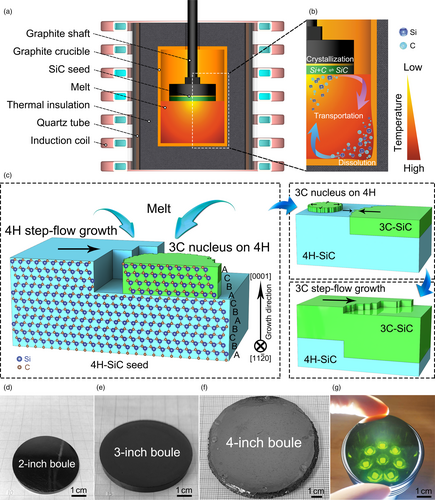
It is reasonable to assume that σ4Hside ≈ σ3Cside because these lateral surfaces form from stacking Si-C bilayers in a similar spacing but in a different sequence, their surface energies will approach equal if averaging the fluctuations of interactions at a macro-scale. σ3C/4H ≈ 0 is a reasonable assumption because of the negligible lattice mismatch between 4H-(0001) and 3C-(111). Therefore, the ΔGhetero is always smaller than the ΔGhomo if the σ3C/Melt − σ4H/Melt < 0. This means that nucleation and crystal growth are favored for 3C- than for 4H- if the difference between ΔGhomo − ΔGhetero is large enough. It is expected that 3C- nucleation easily occurs on 4H- substrate and its step flow is faster than that for 4H-, leading to the total coverage of 3C- on 4H- substrate. Then, the growth of 3C- will proceed steadily. Figure 1c schematically describes the possible route for the phase transition starting from preferential hetero-nucleation to subsequent growth for 3C-SiC single crystal on the condition that it has a lower enough interfacial energy with melts. In this study, it is found that the σ3C/Melt − σ4H/Melt is negative enough when N2 partial pressures () above the melt is over 15 kPa, justifying the above arguments and expectations. Figure 1d–f and Figure S2a,b, Supporting Information show the photographs for 2–4-inch 3C-SiC crystal boules grown under of 20 kPa, respectively. The thickness varies between 4.0 and 10.0 mm in an 84 h-long growth duration (Table 1). The growth rate is about 50–113 μm h−1, a little bit lower than 150 μm h−1 for the PVT method.[21] The 1 mm thick wafers are black in color (Figure S2, Supporting Information) because of high carrier density introduced by N-doping. It is green color under strong light (Figure 1g).[31]
| Growth method | Diameter (inch) | Thickness (mm) | FWHM of XRC (arcsec) | SF density (cm−1) | Resistivity (mΩ·cm) |
|---|---|---|---|---|---|
| TSSG | 2–4 | 4.0–10.0 | 30.0 | 92.2 | 0.58 |
2.2 Properties and Defect Study of 3C-SiC
Raman scattering measurements are performed on a total of 20 sites across the entire wafer surface. All spectra are nearly the same, only the peak at 796 cm−1 is present (Figure 2a,b). The peak is assigned to be the 3C-SiC's transversal optical mode (TO).[32-34] Another characteristic mode, the longitudinal optical one (located at 975 cm−1), which is dependent on the carrier density, does not appear. No folded transverse optical modes at 776 and 707 cm−1 for 4H- and 6H-SiC are observed.[34, 35] A small peak (marked by an arrow) at 741 cm−1 are probably due to the stacking faults or stress.[32, 33] To obtain the information on the evolution of the transition from 4H to 3C, we conduct the Raman scattering measurements on a cross section of the grown boule and the results are shown in Figure 2b and Figure S3, Supporting Information. It is clearly seen that the 3C occurs immediately at the upper surface of the seed, following a transition zone (TZ) about 20 μm consisting of both 3C and 4H. The single phase of 3C is maintained throughout the boule. The observation of photoluminescence (PL) at 523 nm (Figure 2c) corresponds well to the bandgap of 2.36 eV, further confirming the 3C polytype.
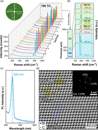
The boule surface is quite flat, but growth steps of 9–22 nm are clearly seen (Figure S4, Supporting Information). Single crystal and powder X-ray diffraction results on small grains cracked from the boule confirm the polytype is 3C with refined lattice parameter a = 4.3563(4) Å (Figure S5, Tables S1 and S2, Supporting Information), similar to the previously reported results.[8] Plan-view high-angle annular dark field scanning transmission electron microscopy (HAADF-STEM) taken on a spherical aberration TEM (Figure 2d) clearly identifies Si and C atoms arrayed in a manner of ABC sequence. The selected area diffraction pattern shown in inset of Figure 2d along zone axis (Z.A.) is well indexed based on a space group of F-43m. Electron energy loss spectrum (EELS) mapping results (Figure S6, Supporting Information) indicate the homogeneous distribution of C and Si at a nanoscale level. Energy dispersive spectroscopy (EDS) mapping results also indicate the homogeneous distribution of Si, C, and N (Figure S7, Supporting Information).
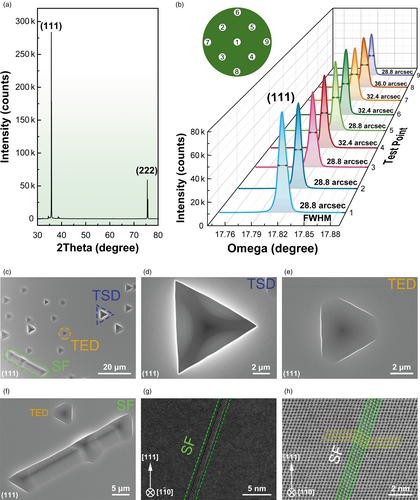
The crystal grows by stacking of (111) crystallographic planes as only diffraction peaks (111) and (222) are present in the θ-2θ scan on the surface of the grown boule, see Figure 3a. To assess the crystallinity of the wafer, we perform the X-ray rocking curve (XRC) measurements. The full width at half maximum (FWHM) for as-grown (111) surface (Figure 3b) ranges from 28.8 to 32.4 arcsec with an average value of 30.0 arcsec (Table 1). The FWHM is very homogeneous across the whole wafer, indicating the high uniformity of 3C-SiC. To our best knowledge, the values stand for the best results on wafers larger than 2-inch obtained so far (Table S3, Supporting Information). Defects are characterized on the wafer after being etched at 500 °C for 10 min in KOH melt. Linear ridges, triangle pits, and rounded-triangle pits are clearly seen on Si-terminated surface under an optical microscope (OM) and a scanning electron microscope (SEM) (Figure 3c–f). The ridges from dozens to more than 100 μm in length are due to the stacking fault (SF) (Figure 3c,f, Figure S8, Supporting Information), a common defect in 3C-SiC.[9, 24, 36, 37] The thickness of typical SFs revealed by the bright-field and dark-field TEM images (Figure 3g,h) is three layers of (111) planes. Its density, defined by the total length of all SFs divided by the observed area, is averaged to be 92.2 cm−1 (Table 1, Figure S9, Supporting Information), much less than what is previously reported (Table S4, Supporting Information). Our results are in good agreement with the reported results that N-doping can substantially increase the SFs length.[38] In addition, the SFs, seen from a slice of 3C-SiC, are delimited by two triangle pits or two rounded-triangle pits (Figure S10, Supporting Information). The typical triangle pits are ~5 μm in size, probably originating from thread screw dislocations (TSDs) (Figure 3c,d). The rounded-triangle pits, a little bit smaller in size, are from thread edge dislocations (TEDs) (Figure 3c,e, Figure S9, Supporting Information).[36, 37, 39-41] They are about 4.3 × 104 cm−2 and 13.9 × 104 cm−2 in density, respectively (Figure S9, Supporting Information). No double-positioning boundaries (DPBs), which are quite common in 3C-SiC,[23, 26, 42-44] are observed in our 3C-SiC wafers.
The electrical characterizations are conducted on a slab crystal cut from the grown boules. Electrical resistivity, carrier density, and mobility are measured by the standard six-wire method (Figure S11, Supporting Information). Figure S12a, Supporting Information shows the variations of electrical resistivity with temperature from 5 to 300 K. We can see that the samples grown under of 15 and 20 kPa exhibit a metallic character. The resistivity decreases with lowering temperature, suggesting the 3C-SiC should become a semi-metal with a room-temperature resistivity of 0.58 mΩ·cm (Table 1, Tables S5 and S6, Supporting Information), much lower than 4H-SiC's (15–28 mΩ·cm) (Table S8, Supporting Information).[45] We note that the crystal grown with of 10 kPa behaves like a semiconductor below about 100 K (Figure S12a, Supporting Information). The carrier density for the 20 kPa sample is calculated to be 1.89 × 1020 cm−3 (Figure S12b, Table S5, Supporting Information), in good agreement with the doping concentration of N (1.99 × 1020 cm−3) measured by secondary ion mass spectroscopy (SIMS) (Figure S13, Supporting Information). It demonstrates that almost all of the doped electrons are activated to the conduction band at room temperature. The calculated mobility ranges from 56.95 to 62.66 cm2 (V·s)−1 (Table S5, Supporting Information). The mobility is enhanced to be 66.24 cm2 (V·s)−1 when the carrier density is lowered (Figure S12c, Tables S5–S7, Supporting Information), meanwhile the resistivity mounts up to 5.77 mΩ·cm, about one fourth of 4H-SiC's (15–28 mΩ·cm) at room temperature,[45] which is much lower than the reported results (Table S8, Supporting Information). In this case, the PL at about 523 nm due to the band-edges transition is observed, as stated above, see Figure 2c.
2.3 Growth Mechanism for 3C-SiC
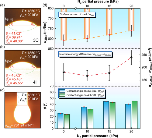
It is easily obtained that the interfacial energies for 3C and 4H are σ3C/Melt 4 = 2151.11 ± 21.90 mN m−1 and σ4H/Melt 4 = 2390.89 ± 19.50 mN m−1 (Table S9, Supporting Information), where σSiC is estimated from the results by Ramakers et al.[28] Figure 4d shows the variations of melt surface tension, the contact angles of melt on substrates and the calculated interfacial energy between the melt and 3C-(111) and 4H-(0001) single crystals based on Young's equation with measured for many times (Figures S14 and S15, Supporting Information). The melt's surface tension decreases as increasing , which can be attributed to the dissolved N in the melt (Figure S16, Supporting Information). We can see that interfacial energy between the melt and 3C-(111) is lower than that for 4H-(0001), and their difference widens with the increasing . Our results indicate that other polytype inclusions are present when the is below 15 kPa. Optimal pressures of above 15 kPa are required to stabilize the 3C polytype during the growth. We then regrow the crystal on a 3C-SiC seed using the same compositions of flux under 20 kPa N2 again. Raman scattering measurements confirm the 3C polytype (Figure S17, Supporting Information).
3 Conclusion
In summary, we found that the nucleation and crystal growth are favored for 3C than for 4H if the difference between the σ3C/Melt − σ4H/Melt is negative enough by the modification of the melt surface tension, beyond what is expected by classic nucleation theory. This led to the growth of high-quality and wafer-scale bulk 3C-SiC single crystals via TSSG. The diameter and the thickness of the 3C-SiC ingot is 4-inch and 4.0–10.0 mm, respectively. More importantly, this TSSG route provides a reliable method to grow high-quality wafer-scale 3C-SiC, exhibiting the potential for further mass production. The grown 3C-SiC single crystals show high crystallinity, high conductivity, and availability, which are very suitable for homogeneous epitaxy and device fabrication. Better homoepitaxy 3C films and the power devices are expected to be fabricated, and thus boost the SiC industry further. Alteration of interfacial energy reported here could be applied to other layered materials to obtain the single crystals that otherwise are difficult to grow.
4 Experimental Section
Experimental details are provided in the Supporting Information.
Acknowledgements
G. W. and D. S. contributed equally to this work. This work was supported by the Beijing Municipal Science and Technology Project (Grant No. Z211100004821004), the Special Project on Transfer and Conversion of Scientific and Technological Achievements of the Chinese Academy of Sciences (Grant No. KFJ-HGZX-042). We thank Y. S. from Institute of Physics, Chinese Academy of Sciences (IOP, CAS) for the single crystal XRD measurement; S. J. and M. H. from IOP, CAS for the discussion of the single-crystal XRD results; Qinghua Zhang from IOP, CAS for the help of TEM measurements; Z. Z., G. Z., L. Y., and C. P. from Beijing Lattice Semiconductor Co., Ltd. for technical help.
Conflict of Interest
The authors declare no conflict of interest.


