Machine Learning-Assisted Fabrication of PCBM-Perovskite Solar Cells with Nanopatterned TiO2 Layer
Abstract
To unlock the full potential of PSCs, machine learning (ML) was implemented in this research to predict the optimal combination of mesoporous-titanium dioxide (mp-TiO2) and weight percentage (wt%) of phenyl-C61-butyric acid methyl ester (PCBM), along with the current density (Jsc), open-circuit voltage (Voc), fill factor (ff), and energy conversion efficiency (ECE). Then, the combination that yielded the highest predicted ECE was selected as a reference to fabricate PCBM-PSCs with nanopatterned TiO2 layer. Subsequently, the PCBM-PSCs with nanopatterned TiO2 layers were fabricated and characterized to further understand the effects of nanopatterning depth and wt% of PCBM on PSCs. Experimentally, the highest ECE of 17.338% is achieved at 127 nm nanopatterning depth and 0.10 wt% of PCBM, where the Jsc, Voc, and ff are 22.877 mA cm−2, 0.963 V, and 0.787, respectively. The measured Jsc, Voc, ff, and ECE values show consistencies with the ML prediction. Hence, these findings not only revealed the potential of ML to be used as a preliminary investigation to navigate the research of PSCs but also highlighted that nanopatterning depth has a significant impact on Jsc, and the incorporation of PCBM on perovskite layer influenced the Voc and ff, which further boosted the performance of PSCs.
1 Introduction
Machine learning (ML), which belongs to an important branch of artificial intelligence, has gained fame in the fields of energy materials and solar cells.[1] ML is a science of getting computers to perform tasks without being explicitly programmed, and it can learn from past results and provide fast predictions of unknown results.[2] Furthermore, ML also can infer the potential rules and relationships among materials, and between materials and the features of the complex system composed of materials only through the data itself without knowing the physical laws.[3] With the proven capabilities of ML, ML can have a significant impact to greatly increase the speed of doing research in perovskite solar cells (PSCs). To optimize PSCs, the conventional method mostly depends on trial-and-error methods, which is not only time-consuming but also has limited test options and leads to the cost of opportunity loss by doing something else with the available time. Therefore, by applying ML, researchers may examine a tremendous amount of data on PSCs and make predictions by uncovering patterns and relationships in the data. These predictions can then be used to guide experiments, enabling researchers to optimize the development of PSCs more efficiently than traditional methods.[4, 5]
Studies have shown that the performance of PSCs is hindered by low-light harvesting. Specifically, the ability of PSCs to absorb light drops significantly between 650–800 nm and diminishes further when the wavelength exceeds 800 nm.[6-8] To overcome this issue, one of the strategies that has been implemented is light scattering. The basic idea of light scattering is to confine light propagation and extend the traveling distance of incident light within the photoelectrode film,[9] which can be explained using Rayleigh and Mie scattering theories. In general, Rayleigh scattering theory is applicable for small-sized particles, whose diameter is less than about one-tenth the wavelength of the incident light while Mie scattering theory is applicable to large particles, whose diameter is larger than the wavelength of the incident light.[10] Apart from that the introduction of nano/microstructures at the glass/air interface has also been reported to increase the incident photon and the generation of photocurrent.[11, 12] Studies also reported that constructing nano/microstructures at the fluorine-doped tin oxide (FTO)/titanium dioxide (TiO2) interface can increase the absorption length for the incident light due to the diffraction effect.[13-15] Therefore, to increase the light harvesting property in PSCs, Hwa-Young Yang et al. have also shown the relationship between the transmittance and the electron generation by varying the nanopatterning depth of the mesoporous titanium dioxide (mp-TiO2) layer.[16]
Next, to improve the electron transport in PSCs, a plethora of materials have been studied and carbon nanomaterials have been widely utilized in PSCs to enhance both the efficiency and stability due to their outstanding chemical, electrical, and mechanical characteristics. It has not only been used as an additive but has also acted on potential structure alternatives for the charge carrier transportation layer, electrode, and active film.[17] Among carbon nanomaterials, fullerene nanometric-sized spherical shapes play an important role for efficient interfacing with perovskites, resulting in a homogeneous distribution of the carbon nanomaterials on the surface of light absorber, thus generating highly selective contacts for electron extraction. Phenyl-C61-butyric acid methyl ester (PCBM), which is a fullerene derivative of the C60, is among the most employed carbon nanomaterials in PSCs due to the alignment of energy levels and high electron mobility.[18, 19] Previous research has demonstrated that by controlling the amount of PCBM in the lead(II) iodide (PbI2) precursor solution, the fill factor (ff) increased significantly as PCBM are able to fill in the pinholes and vacancies between perovskite grains that produce continuous pathways for electron extraction. Moreover, when PCBM was mixed with perovskite to create a PCBM-perovskite structure, the charge recombination lifetime and carrier diffusion length increased as the electron was transported over longer distances in the film compared to pure perovskite film.[20]
Based on the mentioned articles, studies have shown that the most optimized nanopatterning depth will affect the current density (Jsc), and the incorporation of PCBM into perovskite is able to significantly enhance the ff of the PSCs. Therefore, with the potential of ML to be used as a preliminary approach, it is expected that the combination of ML with light management and electron transport strategies will yield a better performance of PSCs. Herein, ML is used to assist the fabrication of PCBM-PSCs with nanopatterned TiO2 layer by deciphering the relationship between nanopatterning depth of mp-TiO2 and weight percentage (wt%) of PCBM to predict the optimal combination of the two variables. Not only that, the photovoltaics parameters, that are Jsc, open-circuit voltage (Voc), ff, and energy conversion efficiency (ECE) are also predicted by the ML. Subsequently, the PCBM-PSCs with nanopatterned TiO2 layer are prepared and characterized to further understand the effects of nanopatterning depth and wt% of PCBM on PSCs. Hence, these findings not only revealed the potential of ML to be used as a preliminary investigation to navigate the research of PSCs but also highlighted that nanopatterning depths have significant impact on Jsc, and the incorporation of PCBM on perovskite layer influenced the Voc and ff, which further boosted the performance of PSCs.
2 Results and Discussion
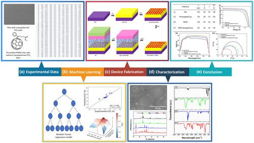
Figure 1 shows the overall scheme of using ML to assist the fabrication of PCBM-PSCs with nanopatterned TiO2 layer. The present process involves the collection of experimental data with the Jsc, Voc, ff, and ECE values for PSCs with nanopatterned TiO2 layer and PCBM-PSCs as listed in Tables S1 and S2, Supporting Information. The nanopatterning depth of PSCs with nanopatterned TiO2 layer were varied to 70, 75, 80, 87, 92, 97, 102, 107, 112, 117, 122, 127, 132, 137, 142, 147, 152, 157, and 167 nm while the wt% of PCBM for PCBM-PSCs were varied to 0.01, 0.03, 0.05, 0.07, 0.10, 0.12, and 0.15 wt%. Subsequently, the dataset was used to predict the optimal combination of nanopatterning depth and the wt% of PCBM, as well as the Jsc, Voc, ff, and ECE of the PCBM-PSCs with nanopatterned TiO2 layers. To achieve that goal, a Random Forest (RF) regression model, which is an ensemble method that uses multiple decision trees to improve the prediction accuracy and prevent overfitting, was used.[21] Then, the optimal combination of nanopatterning depth and wt% of PCBM that yielded the highest ECE was selected as a reference to fabricate the PCBM-PSCs with nanopatterned TiO2 layer. After the fabrication process, the device was characterized to further understand the effects of nanopatterning depth and wt% of PCBM on PSCs. Lastly, the conclusions were deduced based on the results obtained throughout the process.
As demonstrated in Figure 2, the RF regression models were utilized to predict the performance metrics of photovoltaic parameters, including the Jsc, Voc, ff, and ECE. The performance of the RF model was evaluated by using the coefficient of determination (R2) and mean squared error (MSE). The R2 values provide information on how much of the variance is due to the independent variables[22] while MSE is used to evaluate the quality of fit in terms of distance of the regressor to the actual training points.[23] The bound for R2 value is (−∞, 1], where −∞ indicates the worst output value and 1 indicates the best value. In other words, an output value of R2 close to 1 suggested a good prediction of the regression model. For MSE, the value is bounded between [0, +∞) and 0 MSE value is obtained if the linear regression model fits the data perfectly.[24]
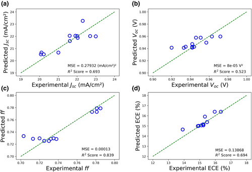
In these predictions, the R2 values obtained for Jsc, Voc, ff, and ECE were 0.693, 0.523, 0.839, and 0.694, respectively, and showed that the RF model can explain 69.3%, 52.3%, 83.9%, and 69.4% of the variation in the Jsc, Voc, ff, and ECE with the input features (nanopatterning depth of mp-TiO2 layer and wt% of PCBM). High R2 values for Jsc, ff, and ECE indicate that the RF model effectively captures the relationship between the input features with Jsc, ff, and ECE, showing the ability of the model to predict accurately. Although the R2 value for the Voc prediction is the lowest among the four parameters, it does not necessarily indicate that the RF model is less accurate for predicting the Voc, but rather highlights the complex interplay between different factors that influence the performance of the photovoltaic parameters. Despite this, the MSEs for all four parameters were relatively low, suggesting the model can still provide reliable predictions.
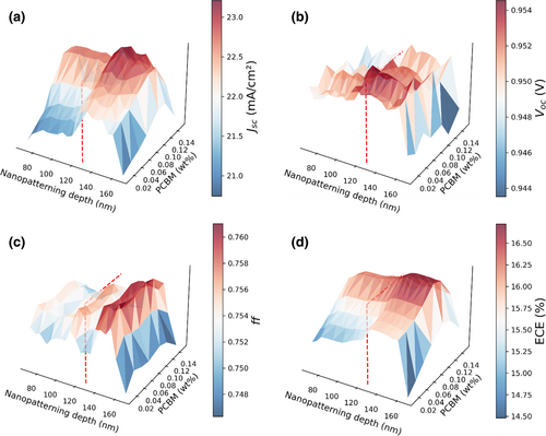
Next, the RF model was further employed to predict the optimal combination of nanopatterning depth and wt% of PCBM for Jsc, Voc, ff, and ECE of PCBM-PSCs with nanopatterned TiO2 layer as shown in Figure 3. The model was trained using the Jsc, Voc, ff, ECE, nanopatterning depths, and wt% of PCBM data of PSCs with nanopatterned TiO2 layer and PCBM-PSCs, that were obtained from previous experiments. The results demonstrated that the highest predicted ECE of 16.73% was achieved with a combination of 127 nm nanopatterning depth and 0.1 wt% of PCBM. The top ten predicted results are also tabulated in Table 1.
| Nanopatterning depth [nm] | wt% of PCBM [wt%] | Jsc [mA cm−2] | Voc [V] | ff | ECE [%] |
|---|---|---|---|---|---|
| 127 | 0.10 | 23.16 | 0.95 | 0.75 | 16.73 |
| 127 | 0.12 | 23.16 | 0.95 | 0.75 | 16.58 |
| 132 | 0.10 | 22.73 | 0.94 | 0.74 | 16.27 |
| 137 | 0.10 | 22.53 | 0.94 | 0.75 | 16.27 |
| 142 | 0.10 | 22.53 | 0.94 | 0.75 | 16.26 |
| 147 | 0.10 | 22.60 | 0.94 | 0.75 | 16.25 |
| 152 | 0.10 | 22.19 | 0.94 | 0.75 | 16.23 |
| 157 | 0.10 | 22.21 | 0.94 | 0.74 | 16.23 |
| 127 | 0.07 | 22.83 | 0.95 | 0.75 | 16.22 |
| 132 | 0.12 | 22.73 | 0.94 | 0.74 | 16.12 |
Graphs in Figure S1, Supporting Information represent the experimental values for the PCBM-PSCs with nanopatterned TiO2 layer at different combinations, and the results in Table S3, Supporting Information show the experimental data for the top three predicted combinations. Next, to have a better understanding regarding the effects of nanopatterning depth and wt% of PCBM on PSCs, and the differences between each PSC, four types of PSCs were fabricated, as shown in Figure S2, Supporting Information. The fabricated PSCs were pristine PSCs, PSCs with nanopatterned TiO2 layer, PCBM-PSCs, and PCBM-PSCs with nanopatterned TiO2 layer. The optimal combination of nanopatterning depth (127 nm) and wt% of PCBM (0.10 wt%) that yielded the highest ECE was selected as a reference to fabricate the PSCs.
Figure 4a shows the field emission scanning electron microscopy (FE-SEM) image of the nanopatterned Si master with 250 nm pore sizes and 250 nm interpore distances. For duplication of nanopatterning on the Si master, the PFPE resin was coated on the surface of Si master and polymerized by UV irradiation for hardening, as shown in Figure 4b. A polyethylene terephthalate (PET) film was used as a flexible substrate of PFPE resin. Figure 4c visualizes the form of the nanopatterned TiO2 with a 280 nm pore size, which looks like the moth-eye nanostructure. The depth of the nanopatterned TiO2 layer is 127 nm, as shown in Figure 4d, which is the most optimized nanopatterning depth.[16]
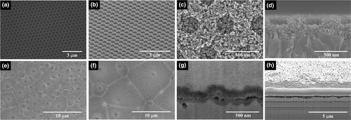
Figure 4e,f show the grain boundaries of perovskite and PCBM-perovskite layers. Without PCBM, the perovskite layer has lots of grain boundaries with smaller grain sizes. However, with the incorporation of 0.10 wt% of PCBM, the grain boundaries decrease significantly, resulting in larger grain size compared to pristine PSC. One explanation for this could be the influence of PCBM in prolonging the crystallization of perovskite, yielding to continuous and denser PCBM-perovskite layer. Previous research also has suggested that the improved surface morphology of PCBM-perovskite layer may be attributed to the possibility of PCBM filling the vacancies between the small grain sizes. This phenomenon may be associated with the incorporation of PCBM as PCBM can move around to alleviate the compressive stress caused by the volume expansion, and therefore, fill in the vacancies in the PCBM-perovskite layer.[20] As a result, the grain of perovskite with PCBM has larger sizes and higher density, that indicates better surface morphology of PCBM-perovskite layer and better stability.[25]
The cross-sectional image of PCBM-perovskite layer on the PCBM-PSCs with nanopatterned TiO2 layer can be observed from Figure 4g. From the FE-SEM images, the PCBM cannot be confirmed because the resolution of FE-SEM was out of range. Thus, Fourier transform infrared (FTIR) analysis was used to verify the PCBM, which will be discussed in a later paragraph. The thicknesses of nanopatterned TiO2 layer, perovskite, spiro-OMeTAD, and Au are 131, 400, 250, and 290 nm, respectively, as shown in Figure 4h.
The x-ray diffraction (XRD) patterns displayed in Figure S3, Supporting Information show that nanopatterning did not change the crystallinity of TiO2, and the incorporation of PCBM did not change the cell dimensions of the perovskite. Both TiO2 and nanopatterned TiO2 show anatase phase at 2θ values of 25.2°, 37°, 38°, 38.5°, 48°, 54°, 55°, and 63°, corresponding to the (101), (103), (004), (112), (200), (105), (211), and (118) peaks.[16, 26] For the PCBM-perovskite layer, both pure perovskite and PCBM-perovskite layers exhibited diffraction peaks at 2θ values of 14.15°, 20.05°, 23.5°, 24.6°, 28.47°, 31.94°, 35.3°, 40.66°, and 43.12°, corresponding to the (110), (112), (211), (202), (220), (310), (312), (224), and (314) crystal planes of tetragonal perovskite, respectively.[27] The results verified that the crystalline PCBM-perovskite was well formed on the nanopatterned TiO2 layer, thus it could achieve better ECE.
Apart from that, the formation of PCBM on the PCBM-perovskite layer was further supported by comparing the FTIR spectra of FTO, perovskite/FTO, PCBM/FTO, and PCBM-perovskite/FTO as represented in Figure S4, Supporting Information. The peaks at 3200 and 3100 cm−1 are due to the N-H stretching vibration for primary amines, and the 1600 and 1475 cm−1 double bands belong to the C=C group. The C-N stretching absorption that occurs in the region from 1250 to 1000 cm−1 indicates the aliphatic amines[28] while the single band at 900 cm−1 is corresponding to the metal iodide stretching vibration,[29] as shown in Figure S4b, Supporting Information. Furthermore, the incorporation of PCBM in the PCBM-perovskite layer was confirmed by comparing Figure S4c,d, Supporting Information. The absorption bands for PCBM can be observed near 3000 cm−1, which indicates the sp3 C-H absorption of alkanes group while the absorption bands for C=O and C-O that appear within the range of 1750–1735 and 1300–1000 cm−1 indicate that the compound is an ester. The peak at 1465 cm−1 is due to the CH2 bending absorption, which is the characteristic of methylene group[28] and the peak at 524 cm−1 belongs to C60.[30] It can be seen that the main characteristic peaks of perovskite and PCBM can be identified in Figure S4d, Supporting Information, which indicate the good formation of the PCBM-perovskite layer.
To have a better insight on the performance of pristine PSC, PSC with nanopatterned TiO2 layer, PCBM-PSC and PCBM-PSC with nanopatterned TiO2 layer, the fabricated devices were characterized and the Jsc, Voc, ff, and ECE of the PSCs are summarized in Table 2. However, instead of choosing the highest ECE for each type of PSCs, the results summarized in Table 2 were chosen based on the most occurring values in the dataset. From the histograms and Gaussian curves plotted in Figure S5, Supporting Information, it can be observed that the central tendencies of ECE for pristine PSC, PSC with nanopatterned TiO2 layer, PCBM-PSC and PCBM-PSC with nanopatterned TiO2 layer are around 13%, 15%, 16% and 17%, indicating that PCBM-PSC with nanopatterned TiO2 layer have a higher tendency to dominate the highest ECE compared to other PSCs. Table S4, Supporting Information presents the highest ECE obtained for PCBM-PSCs with nanopatterned TiO2 layer is 18.518%. However, as the central tendency of PCBM-PSCs with nanopatterned TiO2 layer is around 17%, an ECE value of 17.338% was chosen to represent the overall results.
| Perovskite solar cell | Jsc [mA cm−2] | Voc [V] | ff | ECE [%] |
|---|---|---|---|---|
| (a) Pristine | 20.203 | 0.920 | 0.704 | 13.085 |
| (b) PSCs with nanopatterned TiO2 layer | 22.302 | 0.942 | 0.730 | 15.336 |
| (c) PCBM-PSCs | 21.865 | 0.961 | 0.783 | 16.453 |
| (d) PCBM-PSCs with nanopatterned TiO2 layer | 22.877 | 0.963 | 0.787 | 17.338 |
Moving forward to the graphs presented in Figure 5, it can be clearly observed that the PCBM-PSC with nanopatterned TiO2 layer has the best performance compared to other PSCs. However, to have a clearer grasp regarding the factors that mainly influence the Jsc, Voc, ff, and ECE of the PCBM-PSC with nanopatterned TiO2 layer, the performance of PSC with nanopatterned TiO2 layer and PCBM-PSC will be compared. From the J-V curves presented in Figure 5a, the Jsc (y-axis) of PSC with nanopatterned TiO2 layer is higher compared to PCBM-PSC. On the contrary, the Voc (x-axis) of PCBM-PSC is higher compared to PSC with nanopatterned TiO2 layer. These results suggested that the better performance of PCBM-PSC with nanopatterned TiO2 layer is attributed to the nanopatterning depth that affects Jsc and the wt% of PCBM that influences Voc.
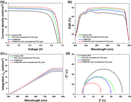
The impact of nanopatterning depth on Jsc was further supported by the EQE spectra. As visualized in Figure 5b, the intensity of the PSC with nanopatterned TiO2 layer at wavelengths ranging from 350 to 800 nm is higher than the PCBM-PSC. When the nanopatterned structure was added onto the surface of mp-TiO2 layer, the optical path length is elongated which resulted in enhanced performance of PSCs. The reason is elongated path length would provide greater distance for the unabsorbed photon to travel, yielding to a greater probability of photon absorption.[31] As illustrated in Figure S6, Supporting Information, without nanopatterning, the solar cell may have an optical path length of one device thickness, but with nanopatterning, the solar cell may have an optical path length equivalent to more than one device, due to the back and forth bouncing of light within the cell many times. Therefore, with greater absorption, the collection of the photogenerated charge carriers would be better, which improved the Jsc and the performance of the solar cell.
Then, the characterization was further conducted by measuring the transmittance of pristine PSCs and PCBM-PSCs with nanopatterned TiO2 layer, as shown in Figure S7, Supporting Information. For wavelengths higher than 350 nm, the transmittance of PCBM-PSC with nanopatterned TiO2 layer was higher than the pristine PSC, implying that the nanopatterned PSCs have stronger absorption compared with the non-nanopatterned PSCs. The transmittance enhancement was due to the rougher surface of PCBM-PSC with nanopatterned TiO2 layer compared to the pristine PSC, which might induce the changes in the refractive index.[16] Furthermore, if the angle of reflected-diffracted light is larger than the critical angle, it causes the total internal reflection because of the decrement in the refractive index values from the TiO2 to the air.[32] Thus, the lower the refractive index, the higher the transmittance.[33]
Through the incorporation of PCBM into the perovskite layer, PCBM can facilitate the charge transport process of PCBM-PSCs with nanopatterned TiO2 layer, due to the mixing of electron-donating perovskite material and the electron-accepting PCBM. When the perovskite absorbs light and generates exciton, the p-orbitals in the phenyl rings of PCBM can align with the p-orbitals of another PCBM, facilitating the π-π interactions. The π-π interactions between PCBM help in exciton separation as these interactions contribute to the formation of electron transfer pathways, enabling efficient electron transport in PSCs. As a result, the electrons will be transferred to the PCBM and can be rapidly moved to the ETL, minimizing the charge recombination. The electrochemical impedance spectroscopy (EIS) characterization shown in Figure 5d and tabulated in Table S5, Supporting Information further supported the results. The series resistance (Rs) can be estimated from the high-frequency intercept on the real axis while the recombination resistance (Rrec) can be assigned to the recombination at the perovskite/TiO2 interface.[34, 35] By analyzing the Nyquist plots, it can be observed that the pristine PSC exhibits the largest semicircle, followed by the PSC with nanopatterned TiO2 layer, PCBM-PSC, and PCBM-PSC with nanopatterned TiO2 layer. The largest semicircle indicates low electron–hole density moves across the perovskite interface,[36] indicating that more charge would take part in the interfacial recombination process.[37] Therefore, as the PCBM-PSC with nanopatterned TiO2 layer has the smallest semicircle, the results indicate that the nanopatterning and PCBM were able to suppress the recombination and increase the electron transport property, owing to the increment in the electron density and the improved surface morphology of PCBM-perovskite layer.
3 Conclusion
In conclusion, ML has been successfully implemented in this research to integrate different factors and predict the optimal combination of nanopatterning depth and wt% of PCBM. The optimal combination predicted was at 127 nm nanopatterning depth and 0.10 wt% of PCBM with Jsc, Voc, ff, and ECE values of 23.162 mA cm−2, 0.953 V, 0.753, and 16.727%. With the assistance of ML, PCBM-PSCs with nanopatterned TiO2 layer were fabricated and characterized. The consistencies of experimental results with the predicted values further validate the reliability of the ML model. Through this approach, it has been observed that nanopatterning depth significantly increased the Jsc, attributed to the improved light harvesting through nanopatterning. The nanopatterned TiO2 layer was able to enhance electron generation, which leads to a higher electron density and thus increases the Jsc. Furthermore, the incorporation of PCBM into the perovskite layer enhanced the electron transport property of PSCs, yielding to the increment in Voc and ff. This is because PCBM were able to fill in the pinholes and grain boundaries between the perovskites, resulting in a formation of larger perovskite-PCBM grain sizes. Experimentally, the highest ECE obtained was 17.338%, which represented a 32.5% improvement compared to the pristine PSC. These results pave the way to understand the effects of nanopatterning depth and wt% of PCBM in the performance of PCBM-PSCs with nanopatterned TiO2 layer and represent a significant step towards the development of PSCs more efficiently by examining and uncovering patterns of the available data through ML.
4 Experimental Section/Methods
Machine learning
Prediction of the most optimal nanopatterning depth and wt% of PCBM in PCBM-PSCs with nanopatterned TiO2 layer
The objective to predict Jsc, Voc, ff, and ECE of PCBM-PSCs with nanopatterned TiO2 layer was formulated as a regression problem, and 108 datasets were used to train the ML model and another 12 datasets were used for validation. The data consist of Jsc, Voc, ff, and ECE for the PSCs with nanopatterned TiO2 layer and PCBM-PSCs that were collected through previous experiments. In this study, a Random Forest regression model was used to train the datasets. Then, the multioutput regressor, which fits one regressor per target, was opted to predict the Jsc, Voc, ff, and ECE, and Optuna was used for hyperparameter tuning and obtaining the most optimal hyperparameter for the model, as shown in Table 3 below.
| Hyperparameter | Optimal value |
|---|---|
| n_estimators | 86 |
| max_depth | 4 |
| max_features | sqrt |
| random_state | 98 |
| min_samples_split | 0.0087 |
Device fabrication
Preparation of perfluoropolyether (PFPE) mold
The PFPE resin (Fluorolink MD700; Solvay Solexis, Milan, Italy) was mixed with 3% w/w photoinitiator (Darocur 1173; Sigma Aldrich, St. Louis, MO, USA) to create the UV-curable resin. Then, the patterned silicon substrate (e.g., Si master) was coated with the UV-curable resin and covered with polyethylene terephthalate (PET) film as a backplane. The PET film was then rolled over to the UV-curable resin to distribute it evenly and the mixture was cross-linked by exposure to UV light at 365 nm for 5 min. After the curing process, the PFPE mold was detached from the Si master.
Preparation of perovskite precursor solution
Methylammonium iodide (MAI) was prepared by mixing 25 mL of methylamine (33 wt% in ethanol; Sigma Aldrich, St. Louis, MO, USA) and 10 mL of hydroiodic acid (55–58%; Kanto Chemical, Tokyo, Japan) in a round-bottom flask, which was kept in an ice bath for 2 h. The resulting product was then obtained using a rotary evaporator at 60 °C for 1 h. After evaporating, the precipitates were recrystallized several times using ethanol (99.9%; Daejung Chemicals, Siheung-si, Korea) and diethyl ether (99%; Daejung Chemicals), followed by an overnight drying at 60 °C in a vacuum oven. Finally, 45 wt% of MAI and lead (II) iodide with a 3:1 molar ratio were stirred in N,N-dimethylformamide (DMF, 99.8%; Sigma Aldrich) at 90 °C for 1 h.
Preparation of PCBM-perovskite precursor solution
The perovskite solution was created by mixing MAI and lead (II) iodide in a 3:1 molar ratio, 45 wt% with DMF. The perovskite-PCBM layer was prepared by dissolving PCBM (99.5%, Nano-C) into chlorobenzene and then mixing the solution with the perovskite precursor solution.
Preparation of hole transport materials (HTM) solution
To prepare the hole transport materials, 73.5 mg of spiro-OMeTA62%; Feiming Chemical Limited, Shenzhen, China), 17 μL of bis(trifluoromethane)sulfonamide lithium salt (Li-TFSI, 99.95%; Sigma Aldrich) solution (574.2 mg of Li-TFSI in 1 mL of acetonitrile), and 36.2 μl of 4-tert-butylpyridine (98%; Sigma Aldrich) were stirred at room temperature for 2 h in 1 mL of chlorobenzene (99.8%; Sigma Aldrich).
Fabrication of PCBM-PSCs with nanopatterned TiO2 layer
The fluorine-doped tin oxide (FTO) glass was cleaned using water, ethanol, and acetone. Then, the compact TiO2 layer was created by spin-coating a precursor solution made of 1 mL of titanium diisopropoxide bis(acetylacetonate; 75 wt% in isopropanol; Sigma Aldrich) in 6 mL of butanol (99%; Daejung Chemicals) onto the FTO at 4000 rpm for 20 s, followed by annealing at 250 °C for 10 min. This process was repeated twice. To form the mp-TiO2 layer, 1 g of TiO2 paste (Ti-Nanoxide T/SP; Solaronix, Aubonne, Switzerland) was diluted in 12 mL of anhydrous ethanol (99.9%; Daejung Chemicals), and spin-coated on a compact TiO2/FTO. After slightly evaporating the solvent by prebaking on a hotplate at 70 °C for 1 min, the PFPE mold was placed on the mp-TiO2/compact TiO2/FTO substrate and heat-pressed for 5 min at 70 °C with a pressure of 2 bar. After removing the mold, the resulting nanopatterned mp-TiO2/compact TiO2/FTO substrate was then annealed at 500 °C for 1 h. The PCBM-perovskite layer was created by spin coating the PCBM-perovskite precursor solution at 3000 rpm onto the nanopatterned mp-TiO2 layer through the hot-casting technique at 90 °C, followed by annealing at 130 °C for 1 h. The HTM layer was spin-coated at 4000 rpm for 60 s and dried overnight in a glovebox. All the procedures were conducted inside a dried air-filled glovebox. Finally, the Au electrode was deposited through thermal evaporation.
Analysis
A field emission scanning electron microscope (FE-SEM, SU-70; Hitachi) was used to examine the morphology and thickness of the device configurations while an X-ray diffractometer (D/max-2500; Rigaku Corp., Tokyo, Japan) was used to confirm the crystallinity of TiO2 and perovskite layers. To measure the transmittance, a UV–Vis spectrophotometer (Jasco International Co., Ltd., V-730, Tokyo, Japan) was used and the infrared spectra were recorded on the Fourier-transform infrared (FTIR) spectrometer (Nicolet 6700, Thermo Scientific) in the range of 600–4000 cm−1. Then, a solar simulator (., Model 94022A; Newport CorpIrvine, CA, USA) with a source meter (Keithley 2400; Keithley Instruments Inc., Cleveland, OH, USA) under AM 1.5 illumination (100 mW cm−2) was used to characterize the photovoltaic properties of PSCs. The characterization was carried out at the Future Energy Convergence Core Center (FECC). All devices were measured by masking 0.1256 cm2 of the active area with a mask under argon condition. The solar cell quantum efficiency measurement system (QEX7; PV Measurements Inc., Point Roberts, WA, USA) was also used to measure the incident photon to electron conversion efficiencies. Electrochemical impedance spectroscopy was performed using a potentiostat (Solartron 1287) and frequency response analyzer (Solartron 1260) in the range of 10−2 and 106 Hz. The measurements were analyzed using the ZView software (Solartron Analytical) with the aid of appropriate equivalent circuit, where the applied bias voltage and the amplitude of alternating current were set at the open circuit voltage (Voc). The impedance measurements were carried out at open-circuit potential under AM 1.5 illumination.
Acknowledgements
S.N.S., H.-Y.Y., J.K., Y.-C.M., G.S.G. contributed equally to this work. This research was supported by the “Human Resources Program in Energy Technology” of the Korea Institute of Energy Technology Evaluation and Planning (KETEP), which received financial resources from the Ministry of Trade, Industry & Energy, Republic of Korea (No. 20204010600470), by the Korea Evaluation Institute of Industrial Technology (KEIT) and the Ministry of Trade, Industry & Energy (MOTIE) of the Republic of Korea (No. 20018608), and by Basic Science Research Program through the National Research Foundation of Korea (NRF) funded by the Ministry of Education (No. 2022R1I1A1A01064236). This research was based on the dissertation by Siti Norhasanah Sanimu at Jeonbuk National University.
Conflict of Interest
The authors declare no conflict of interest.


