Alleviating Interfacial Recombination of Heterojunction Electron Transport Layer via Oxygen Vacancy Engineering for Efficient Perovskite Solar Cells Over 23%
Abstract
Electron transport layer (ETL) is pivotal to charge carrier transport for PSCs to reach the Shockley–Queisser limit. This study provides a fundamental understanding of heterojunction electron transport layers (ETLs) at the atomic level for stable and efficient perovskite solar cells (PSCs). The bilayer structure of an ETL composed of SnO2 on TiO2 was examined, revealing a critical factor limiting its potential to obtain efficient performance. Alteration of oxygen vacancies in the TiO2 underlayer via an annealing process is found to induce manipulated band offsets at the interface between the TiO2 and SnO2 layers. In-depth electronic investigations of the bilayer structure elucidate the importance of the electronic properties at the interface between the TiO2 and SnO2 layers. The apparent correlation in hysteresis phenomena, including current density–voltage (J–V) curves, appears as a function of the type of band alignment. Density functional theory calculations reveal the intimate relationship between oxygen vacancies, deep trap states, and charge transport efficiency at the interface between the TiO2 and SnO2 layers. The formation of cascade band alignment via control over the TiO2 underlayer enhances device performance and suppresses hysteresis. Optimal performance exhibits a power conversion efficiency (PCE) of 23.45% with an open-circuit voltage (Voc) of 1.184 V, showing better device stability under maximum power point tracking compared with a staggered bilayer under one-sun continuous illumination.
1 Introduction
Metal halide perovskites are at the focus point of next-generation optoelectronic materials, realizing solution processing, band gap tuning, and compatibility with various electronic devices.[1-3] Photovoltaics using metal halide perovskites were initiated from the power conversion efficiency (PCEs) of 3.8%,[4] now reached to a certified value of 25.5%.[5] Nevertheless, parasitic ionic reactions occurring at charge-selective layers remain hurdles to be overcome for further improvements in device performance and operational stability, as these interactions cause unsatisfactory device stability and hysteresis in current density–voltage (J–V) curves.[6, 7] The origin factors that contribute to the parasitic chemical reactions are associated with the structure, composition, ionic bonding, and crystal quality of the perovskite;[8] however, the band gap, electron transferability, trap state, and chemical stability of electron transport layers (ETLs) are found to play a significant role in improving the reliability of perovskite solar cells (PSCs).[9-12] Therefore, the chemically dormant metal oxide materials that form an electrical ohmic contact with the perovskite layer are a key component in the development of stable-efficient perovskite photovoltaic technologies.[13-15]
To date, numerous materials have been investigated to replace the commonly used titanium dioxide (TiO2) in PSCs owing to the cell degradation induced by its photocatalytic reaction with the perovskite layer under UV irradiation.[16, 17] Tin oxide (SnO2) stands out as a novel ETL material owing to its desirable features, which may reduce cell degradation, such as a wide band gap, high electron mobility, good chemical stability, and suitable conduction band edge with respect to perovskite materials.[18, 19] Advances in SnO2 ETLs for PSCs in recent studies have resulted in variations in the ETLs that can be classified as monolithic layers, homojunction bilayers, and heterojunction bilayers. Monolithic SnO2 layers are mostly produced via spin-coating methods based on a sol-gel process;[20, 21] these layers have accelerated the research on solar cells with SnO2 materials and reported PCE values as high as 23.56%.[22] However, this technique is prone to generate an imperfect morphology with pinholes and cracks causing nonradiative recombination.[23, 24] In contrast, bilayer structures appear competitive in terms of interfacial engineering for better charge extraction because of the passivation by a sequential layer synergically with enhanced band alignment.[25, 26] Specifically, homojunction bilayers were sequentially constructed by depositing different SnO2 layers.[27, 28] For instance, Anaraki et al. obtained a PCE of 20.7% in PSCs by depositing a subsequent SnO2 layer via chemical bath deposition on a spin-coated SnO2 layer.[29] Gong et al.[30] presented a fluorine-doped SnO2 bilayer ETL with a graded doping concentration, resulting in a PCE of 20.2%. Ye et al.[31] reported a homojunction bilayer ETL for PSCs by combining nanoparticle SnO2 layers of different doping levels with ammonium chloride to achieve a PCE of 21.75% with an exceptional Voc of 1.21 V. Meanwhile, heterojunction bilayers have been proposed wherein a SnO2 layer is stacked onto layered materials with different energy levels to exploit the synergetic effects of each material.[32] Liu et al.[33] stacked aqueous colloidal SnO2 particles onto a highly crystalline dense TiO2 layer, confirming improved charge extraction by the SnO2 layer with a PCE of 18.03%. Song et al.[32] systematically investigated the electronic properties of the structural configuration by employing the concept of a SnO2@TiO2 bilayer and obtained a PCE of 21.1% with anodized amorphous TiO2 as the bottom layer and spin-coated SnO2 as the top layer. Tavakoli et al.[34] reported much-improved electron extraction with reduced nonradiative recombination by replacing crystalline SnO2 with amorphous SnO2 for homojunction bilayers, exhibiting a PCE of 21.65%. Conversely, some groups have studied an alternative underlayer of TiO2 to tune the imperfect energy band alignment with a SnO2 layer. Wang et al.[35] explored a WOx layer as an underlayer because of its appropriate energy level and high electron mobility, leading to a PCE of 20.52%. They further introduced an In2O3 layer deposited by a spin-coating method into a heterojunction bilayer, achieving a PCE of 23.24%.[36] From an engineering viewpoint, a bilayer structure for ETLs using SnO2 as a contact layer has proven its potential with excellent performance. However, in-depth investigation of the intimate relationship between oxygen vacancies, deep trap state, and charge transport efficiency at the interface of heterojunction layers for an electronic understanding of the bilayer structure is still lacking.
This study systematically investigates the bilayer structure of an ETL composed of SnO2 on TiO2 to address a critical factor in forming a graded energy alignment for efficient heterojunction bilayers. The energy band of TiO2 underlayers can be tailored via oxygen vacancy engineering. The influence of the tailored underlayer on the band offset, which describes the relative position of the energy levels, is investigated with respect to the PSC performance. The manipulation of oxygen vacancies in the TiO2 underlayer determines the landscape of energy alignment in the heterojunction bilayer, thereby affecting interfacial recombination. Moreover, atomic reconstruction through oxygen vacancy engineering is evaluated via density functional theory (DFT) calculations to reveal the electronic properties affecting the carrier transport across the junction. Consequently, by implementing oxygen vacancy engineering on the heterojunction bilayer, the PSCs exhibit a best PCE of 23.45% with a high fill factor (FF) of 82.6%, a Voc of 1.184 V, and a Jsc of 23.9 mA cm–2, exerting negligible hysteresis and enhanced device operational stability.
2 Results and Discussion
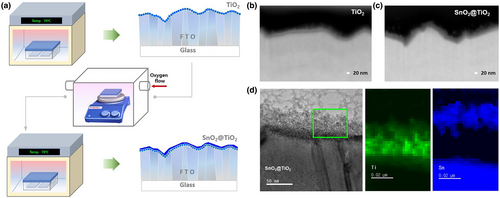
Band alignment in a bilayer structure is significant for the charge transport in photovoltaic devices. Inefficiency in charge transport causes a decrease in device performance via increased nonradiative recombination.[37] TiO2 materials have the advantage of reproducibility as an ETL because they have been studied for more than three decades in DSSCs. However, TiO2 materials have been commonly deemed inappropriate for the bilayer structure because their conduction band (CB) edge is higher than SnO2 materials.[33, 38] To manage the design challenges, this study aimed to develop a heterojunction layer by applying substoichiometric produced metal oxides. In general, metal oxides produced from hydrolysis reactions characterize the amorphous nature and substoichiometric chemical compositions, especially the oxygen ratios, which identify their electronic properties with varied band gaps. Accordingly, heterojunction bilayers were prepared by sequential chemical bath deposition (CBD), which is a scalable method that is applicable to the industry.[39] Figure 1a presents a schematic representation of the deposition process for the heterojunction bilayer in which the TiO2-deposited underlayer (u-TiO2) was treated via a CBD method as an annealing process to control its oxygen vacancies. An amorphous SnO2 layer was then formed via a hydrolysis-regulated CBD method. The morphologies of the films in each process were examined using scanning electron microscopy (SEM) images. The surface was fully covered by a TiO2 layer without pinholes or cracks (Figure S1a), allowing for the formation of a uniform subsequential layer. As shown in Figure S1b, the top SnO2 (t-SnO2) was uniformly deposited, without agglomerated clusters that were easily produced during hydrolysis.[9] Cross-sectional focused ion beam (FIB) SEM images (Figure 1b,c) of the samples revealed the uniform formation of ETLs according to the surface of the fluorine-doped tin oxide (FTO) regardless of the rugged surface of the FTO even at the valley. The estimated thickness was ~25 nm for the u-TiO2, and the total thickness of the heterojunction bilayer was ~40 nm, including the u-TiO2 layer (Figure 1d). The methodological advantage of surface reaction selectivity of CBD enabled the fully covered surface by the ETL. A homogeneous surface is favored for the promotion of perovskite crystal growth and thus contributes to efficient charge transport from the perovskite layer to the ETLs. Further analysis of the u-TiO2 and u-TiO2/t-SnO2 layers for crystal information will be discussed in the later part.
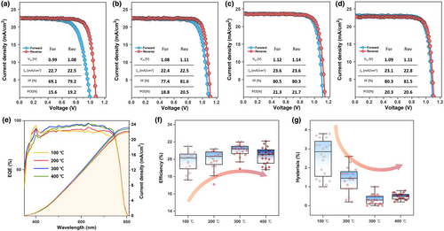
To evaluate the influence of ETLs on perovskite photovoltaics, planar PSCs were fabricated by depositing a triple-cation perovskite layer on the heterojunction bilayers in the FTO/ETL/perovskite/PTAA/Au configuration. A full experimental description of the device fabrication is provided in the fabrication section. The u-TiO2 films treated via oxygen vacancy engineering are denoted as 100, 200, 300, and 400 °C according to their processing conditions. The t-SnO2s for all processes were processed simultaneously. The J–V characteristics of PSCs based on the heterojunction bilayers of u-TiO2/t-SnO2 are shown in Figure 2a–d; their device parameters are shown in the inset. The PCE of the devices increased with the annealing of u-TiO2, presenting the maximum performance at an annealing temperature of 300 °C, which is primarily based on the enhancement in Voc and Jsc. This enhancement could be attributed to the suppressed nonradiative recombination during the transportation of electrons to the electrode. The disparity of the PCEs in the forward scan with respect to the reverse scan increased substantially at 100 and 200 °C, and the FFs appeared to be significantly deteriorated, leading to inferior efficiency in the forward scan. By contrast, negligible hysteresis occurred in the optimum performance group at 300 and 400 °C. The hysteretic effect seemed to lead to lower EQEs than those obtained from the J–V curves (Figure 2e). A summary of the PCEs of the PSCs extracted from the J–V curves in the reverse scan is shown in Figure 2f. The disparity in PCEs between forward and reverse scans is displayed in Figure 2g.
Structural and morphological comparisons were conducted to correlate the influence of the perovskite layers on hysteresis in the J–V curves. SEM images and XRD patterns of the perovskite layers that were deposited on the heterojunction bilayers are shown in Figures S2 and S3. SEM images and XRD patterns of the perovskite films indicate that the perovskite layers have comparable crystal quality regardless of the substrate. This observation corroborates that the surface energy of the t-SnO2 layers exerted at the perovskite layer is consistent for the heterojunction bilayers and possibly originates from the equivalent quality of the t-SnO2 layers.[23]
To elucidate the discrete behavior observed in the PSCs, dark J–V curves were investigated by performing fast J–V scans to obtain sheer electrical signals across a device without the slow time component, which may be related to ionic movement or a slow displacement of charge.[40] Figure 3a–d shows the dark J–V curves of the PSCs measured at a scan rate of 1000 mV s–1. Noticeable electronic characteristics are observed in the rectifying region. The devices that show hysteresis in the J–V curves also exhibit a lower current and hysteresis in the dark J–V curves. The current in the reverse scan showed an S-shape and was smaller than that of the forward scan. Technically, the rectifying current is connected to a Schottky barrier, in which the barrier height controls the current flow. That is, a higher current flow in the rectifying region is likely to have a lower barrier height. The dark J–V curves explain that the contrasting performances in the PSCs can be primarily interpreted as a result of the interfaces that cause an imbalance in charge transport. The magnitude of hysteresis in the dark J–V curves appeared to be directly linked to the interfacial properties of the devices. As indicated in previous reports, the accumulation of ionic species at the interface results in an increase in the barrier height, thus contributing to a decrease in the rectifying current at a certain scan direction.[41, 42] Hence, the hysteresis in the dark J–V curves in the rectifying region can be attributed to the accumulated ionic species or trapped charges at the interface rather than ions in the perovskite layer, which is because the scan rate is too fast for ions in the perovskite layer to participate in electrical conduction.[43] Thus, the characterization of the fast dark J–V curves clearly indicates the underlying role of u-TiO2 in the heterojunction bilayers, which alters the interfacial properties responsible for the device performance.
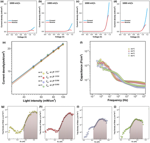
To determine carrier transportation under quasi-steady-state conditions, J–V curves were measured against light intensity, which follows the law that the photocurrent scales linearly with light intensity. The J–V characteristics of the PSCs with respect to light intensity are shown in Figure S4. The Jsc variations with respect to light intensity are plotted in Figure 3e. In general, the slope of Jsc against the light intensity approaches 1 when free carriers are efficiently extracted to the electrodes without trap-assisted recombination. The slopes of the devices at 100 and 200 °C were greater than unity. These values are thought to be associated with the trapping–detrapping process of charges in deep defect states, which are highly sensitive to light intensity.[44] The nonlinear trend of Voc with illumination supports the influence of charges trapped in the defect states.[9] The slopes of 0.996 and 0.993 were obtained for devices at 300 and 400 °C, respectively, with the linearity of Voc. Observing carrier transportation under quasi-steady-state conditions indicated that electronic trap states vary with the heterojunction bilayers, which affects the device performance. In this sense, trap states in devices with different heterojunction bilayers were compared by performing capacitance versus frequency (C–f) measurements in the dark. The piles of electrons in the trap states contribute to the capacitance, responding to the rates of the AC bias.[45] Figure 3f shows the C–f spectra of the devices. The signals can be divided into high- and low-frequency ranges, which are ascribed to capacitances from shallow and deep defects, respectively.[46] The trap density of states (tDOS) was calculated by taking the derivative of the capacitance; the trap distribution was fitted by a Gaussian function.[47] In comparing the results shown in Figure 3f, a deep trap energy level was noted. The fitting results are listed in Table S1. The tDOSs of the devices with a Gaussian distribution are presented in Figure 3g–j. The trap energy levels were 0.601, 0.577, 0.518, and 0.499 eV for the devices at 100, 200, 300, and 400 °C, respectively. Increasing the annealing temperature for oxygen vacancy engineering resulted in a decrease in the deep trap energy level of the devices. In addition, the calculated trap densities were 5.63E17, 2.87E17, 6.53E16, and 7.10E16 cm–3 for devices at 100, 200, 300, and 400 °C, respectively. The trap density of the devices with hysteresis was one order of magnitude higher than that of the other devices. The lowest trap density was observed for the device with a heterojunction bilayer of 300 °C. The variation of trap densities and trap energy levels connected to different engineering processes provided insights into the atomic states of the u-TiO2 and t-SnO2 layers.
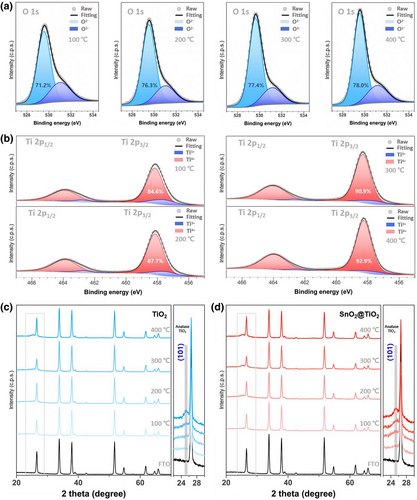
The chemical states of the u-TiO2 and t-SnO2 layers were characterized using X-ray photoelectron spectroscopy (XPS). Figure 4a,b show the XPS peaks of the u-TiO2 films according to the oxygen vacancy engineering conditions for O 1s peaks and Ti 2p3/2 peaks, respectively. The deconvolution of the O 1s peaks demonstrated that the oxygen states in u-TiO2 became increasingly changed with annealing temperature. Peaks related to oxygen in the lattice (O2–) were identically positioned at 529.58 eV, and their area percentage in the O 1s spectrum increased as those of chemisorbed nonlattice oxygen (O1–) decreased. The presence of the O1– peak is related to the incomplete oxidation of the surface, implying that u-TiO2 has non-stoichiometries.[48] The oxidation states of Ti were compared to further interpret the electronic state of the engaging element. The peak area of Ti4+ appeared to gradually increase with decreasing Ti3+ content, which is related to Ti2O3 exhibiting metallic behavior.[49] Previous studies by others demonstrated that the reduction in Ti4+ to Ti3+ is promoted by the loss of oxygen in its bonding.[50] The peaks for Ti 2p3/2 indicate that the u-TiO2 with a Ti3+ chemical state was recovered by oxygen vacancy engineering. For comparison of the chemical states in the t-SnO2 layers, the deconvoluted peaks for O 1s and Sn 3d5/2 are shown in Figure S5. The chemical state of the t-SnO2 layers appeared to be identical regardless of the underlying layers with minimal variation and seemed to be sample-dependent under the experimental conditions. Alterations in their chemical states were potentially corroborated to changes in their crystallography. Thus, XRD analyses were conducted on the corresponding films. Figure 4c shows the XRD pattern of the u-TiO2 films, indicating changes in the (101) diffraction of anatase TiO2 with annealing temperature. The transition from amorphous to semi-crystalline crystallinity was monitored at increased temperatures. No observable changes occurred in the crystallographic system after the deposition of SnO2 on the u-TiO2 films, except for slightly increased amorphous properties that were caused by the nature of the t-SnO2 layers (Figure 4d).
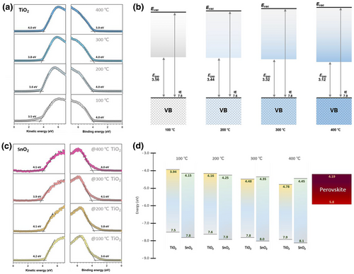
To correlate the observed trends in the chemical state and gain insight into the band profiles in the heterojunction bilayers, ultraviolet photoelectron spectroscopy (UPS) was performed. Figure 5a shows the UPS spectra of the u-TiO2 films near the secondary cutoff and valence band (VB) region. The spectra measured in the secondary cutoff region showed that the WF of the u-TiO2 films linearly increased with annealing temperature, corroborating a dominant contribution from interactions between Ti d and O p orbitals, which agrees well with the XPS results. The change in the Fermi level can be understood as an alteration of the surface electronic state with defect distribution, considering the highly sensitive surface analysis of UPS. Figure 5b shows the band profiles of the u-TiO2 films. The conduction band minimum (CBM) was determined by subtracting the band gap energies of the u-TiO2 films calculated using Tauc plots of the absorbance measurements (Figure S6a). The band gap energies were linearly altered, which was related to the tuning of the underlying crystallographic structure in the bulk phase. This indicates that the band profile of the u-TiO2 film was successfully controlled by oxygen vacancy engineering. Figure 5c shows the UPS spectra of t-SnO2 deposited on u-TiO2. The valence and conduction bands of t-SnO2 were modulated according to the underlayer, indicating that u-TiO2 affects the interfacial electronic profiles of the upper layers. In addition, the band gap energies of t-SnO2 were extracted from Tauc plots (Figure S6b), and the extracted values indicated that the bulk properties of t-SnO2 were comparable regardless of the u-TiO2s, rationalizing their constant bulk quality in all the devices. Figure 5d shows a schematic diagram of the band alignment between the heterojunction bilayer and perovskite in the solar cells, where the band types for ETLs differ according to the u-TiO2 films. Imperfect interfacial band alignment occurred in the CBD of the heterojunction bilayers prepared at 100 and 200 °C for the u-TiO2 film, that is, staggered band alignment. Cascade band alignment was completed in the heterojunction bilayers prepared at 300 and 400 °C for the u-TiO2 film. In particular, the minimum driving force (ΔG) for charge extraction of 0.06 eV, where ΔG = Perovskite.ECBM − SnO2.ECBM, was seen in the heterojunction bilayer prepared at 200 °C. This probably resulted in a higher Voc than in the device with the heterojunction bilayer at 100 °C. However, observed hysteresis and J–V curves indicate a low device performance. The observed low performance and hysteresis characteristics are expected to be related to the staggered band alignment. The lack of a barrier between the u-TiO2 and t-SnO2 layers was attributed to the improved performance and negligible hysteresis in the devices with the heterojunction bilayers prepared at 300 and 400 °C. Although a barrier energy of 0.09 eV between the u-TiO2 and t-SnO2 layers at 200 °C can be inferred as an insignificant value, the barrier can block carrier transport and delay the transport time. This leads to a charge accumulation that can occur between the ETLs with a trapping–detrapping process of charges in the defect states. This phenomenon is likely to adversely affect the balance of the internal electric field, which may trigger the acceleration of ionic movement in the perovskite absorber; thus, the hysteresis characteristic can be dominant in the J − V curves. Our interpretation of these experimental results coincides well with the recent theoretical simulation for understanding the hysteretic behavior in PSCs.[43, 51]
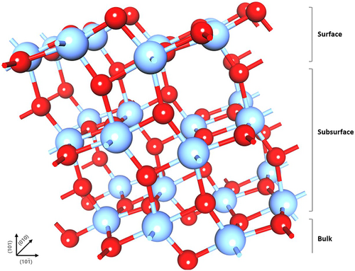
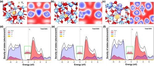
To examine the influence of oxygen defects on the electronic state of u-TiO2 in depth, electronic structure calculations were performed via ab-initio DFT on an anatase TiO2 supercell. To model the anatase TiO2 surface, the (101) plane was exposed to a vacuum in accordance with the XRD results, and the slab model was divided into three layers to understand the dominant defect and the localization state on the correlated surface layer (Figure 6). For comparison, an oxygen vacancy to Ti was created at the equivalently coordinated sites in the surface and subsurface layers. All the models were simulated based on the periodic boundary conditions with a vacuum of ~15 Å. The oxygen vacancy structures created on the surface (VOs) are shown in Figure 7a. The models that have an equivalent oxygen defect in the subsurface layer (VOss1, VOss2) are shown in Figures 7b,c. The defect properties were evaluated by calculating their formation energies under oxygen-rich conditions. Table S2 lists the relative parameters before and after geometry relaxation in the pristine anatase (101) slab. The defect formation energies at different sites in anatase (101) were 5.14 for VOs, 5.11 for VOss1, and 4.73 eV for VOss2. The calculated formation energies of oxygen vacancy defect are consistent with the results from the screened exchange (sX) hybrid functional method.[52] A comparison of the formation energy of the oxygen vacancy showed that the subsurface oxygen vacancy, VOss2, requires less energy to be created on the anatase surface than other vacancies. As previously reported, the formation of an oxygen vacancy in the TiO2 surface structure results in two unpaired electrons.[53] To determine the state of the unpaired electrons, the charge density was overlaid to the models, as shown on the left of Figure 7a−c. Electron–polaron formation was confirmed at Ti sites neighboring the vacancy in the case of subsurface oxygen vacancies, whereas no polaron was observed for the VOs structure. In particular, the VOss2 exhibited two polaron formations at the surface layer with an additional polaron at the next-nearest Ti neighboring the vacancy, plausibly increasing the potential barrier energy at the anatase (101) surface.[54] To examine the polaron formation, electron localization was considered, as depicted on the right of Figure 7a−c. Excess electrons were created with the removal of an oxygen ion on the surface, and VOs was stabilized by local geometrical constraints; thus, no localization occurred at Ti sites neighboring the vacancy. Localization of electrons was identified in the VOss1 and VOss2 structures at the Ti sites with polarons, indicating the reduction in Ti4+ to Ti3+. The VOss1 structure demonstrated that one electron was localized, and one was partially delocalized. Fully localized states of the two electrons appear in the VOss2 structure. The energy states of the three defects were compared by projecting the density of states (DOS), as shown in Figure 7d−f. The presence of an oxygen vacancy in the structures shifts the Fermi level (Ef) to the conduction band compared to that of the pristine surface (Figure S7). The conduction properties and gap states were modified by oxygen vacancy positions. The oxygen vacancies in the subsurface at the terrace position, VOss2, produced a double peak at the gap state, possibly due to the interaction of two occupied Ti 3d orbitals. The energy of the gap state is situated at 0.6 eV lower than the Ef, which is expected to act as defect sites for electron trapping. The obtained energy value for the electron trapping state supported the result of the deep trap energy in the devices, indicating that the oxygen vacancy state of u-TiO2 in the heterojunction bilayer plays a significant role in improving the device performance.
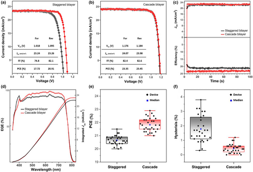
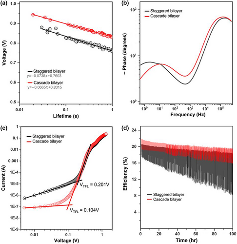
Recently, additional surface treatment onto the perovskite layer has emerged as a credible and necessary strategy for perovskite defect passivation. To scrutinize the interfacial influence of the band types of the corresponding heterojunction bilayer in efficient perovskite solar cells, octylammonium iodide (OAI) was deposited onto the perovskite layers.[55] The J–V curves of the best-performing devices, shown in Figure 8a,b demonstrates that the device with the cascade bilayer exhibited a PCE of 23.45%, which was enabled by a high Voc of 1.184 V, a Jsc of 23.98 mA cm–2, and an FF of 82.6%. The device with the staggered bilayer showed a PCE of 20.91% with a Voc of 1.095 V, a Jsc of 23.26 mA cm–2, and an FF of 82.1%. Although the addition of a passivation layer correlated with performance improvements for both devices, the device with staggered bilayer still exhibited hysteresis. This is attributed to charge trapping at the defect state in the u-TiO2 and to imperfect heterojunction band alignment.[9] Accordingly, synergetic improvement by the passivation layer was strengthened in the device with the cascade heterojunction bilayer. Their performance was substantiated by measuring at the maximum power point (MPP), as shown in Figure 8c, corresponding to PCEs of 21.0 and 23.5% for those devices, respectively. Faster carrier extraction in the cascade bilayer-based device was confirmed by recording a very short transient time for the current to stabilize upon illumination. The integrated current density calculated from the EQE spectra (Figure 8d) showed a value that matched the J–V curves within a difference of 5%. Staggered bilayer-based devices exhibited a narrow distribution in the PCEs at reverse scan (Figure 8e); however, in a device-by-device comparison and in contrast to the cascade bilayer-based devices, they showed a significant divergence in PCEs between forward and reverse scans (Figure 8f). Charge carrier lifetimes were compared by recording open-circuit voltage decay (OCVD) in the linear region (Figure S8a), and their decay as a function of time is plotted in Figure 9a. The slope of the carrier recombination obtained by fitting showed suppressed recombination. To quantitatively compare the carrier lifetimes in the devices, the charge transport dynamics were investigated using electrochemical impedance spectroscopy (EIS) under quasi-steady-state conditions (Figure S8b), and the Nyquist plots were converted into phase versus frequency Bode plots, as shown in Figure 9b. The time constants of the nonradiative recombination extracted from the high frequency at the peak maximum (τ = 1/2πfm) were 1051ns for the cascade bilayer-based device and 830 ns for the staggered bilayer-based device.[56] The impedance signal at a low frequency is related to the dynamic response of the interfacial phenomena at the ETLs of the perovskite layer.[57] Interestingly, a double turning point occurred at a low frequency in the staggered bilayer-based device. This can be interpreted as signals involved in two types of capacitor-like kinetics at the ETLs, potentially caused by the staggered band alignment in the heterojunction bilayer.[9] The bias-dependent current was evaluated with electron-only devices to measure the trap-filled limit voltage (VTFL) (Figure 9c), which is directly proportional to the trap density (Nt = 2εε0VTFL/qL2), where q is the elementary charge, L is the thickness of the active layer, ε is the dielectric constant, and ε0 is the vacuum permittivity.[58] The VTFL of the cascade bilayer-based device was almost twice the value of 0.104 V. Operational stability tests were performed with the unencapsulated devices at the MPP under continuous one-sun illumination. Figure 9d shows the tracking records by sweeping near the MPP. The cascade bilayer-based device retained a range of 10% of the initial efficiency during measurement, whereas the staggered bilayer-based device showed an unstable efficiency tracking record, which became significantly worse over time. The operational stability test emphasizes band alignment between the bottom and top layers in a bilayer configuration for better stability and enhanced device performance.
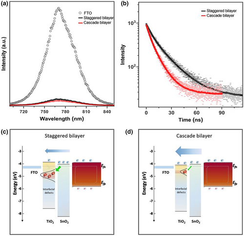
The delicate dependence of charge extraction on the ETLs was further examined via steady-state photoluminescence (PL). Figure 10a shows the PL spectra of the perovskite film on the ETLs. Better quenching characteristics were observed for the PL emission on the cascade bilayer. To further resolve the PL decay kinetics in real time, the quenching properties were evaluated using a time-correlated single-photon counting (TCSPC) system. The results are indicated in Figure 10b. The kinetic parameters, which were evaluated using a bi-exponential function, are listed in Table S3. Although the weight fraction that expresses the dominance ratio of each decay component was comparable for those samples, the decay time for each component showed faster decay in the perovskite film on the cascade bilayer than the staggered bilayer-based device. This implies that enhanced charge transport by graded band alignment in the heterojunction bilayer prevents carrier accumulation from sluggish electron transport, thus alleviating nonradiative recombination at the interface. Figure 10c,d illustrate schematic diagrams of electron transport in different band-aligned heterojunction bilayers. An energy barrier caused by the height of the CBM alignment in the heterojunction bilayer interrupts electron transport, leading to charge accumulation and increased possibility of charge trapping in deep defect states in the t-TiO2 layer (staggered bilayer). By contrast, better transport by cascade band alignment allows photogenerated charges to be efficiently transported to the electrode with less possibility for charge trapping in the deep defect states (cascade bilayer).
3 Conclusion
In summary, this study demonstrates a simple and effective atomic reconstruction for an efficient TiO2/SnO2 heterojunction bilayer. The atomic reconstruction of the TiO2 underlayer tailors the band offset across the heterojunction, which effectively alters the band alignment. The presence of Ti3+ in TiO2 leads to a deep trap state, which is unlikely to be passivated by the top layer owing to its preferential position on the subsurface layer. Moreover, the electronic state of the TiO2 underlayer can manipulate the hysteretic behavior in heterojunction bilayer-based devices, which is corroborated by multiple comprehensive characterizations of atomic configuration, electron localization function, electronic measurement, trap calculation, and impedance spectroscopy. Eventually, the successful formation of cascade energy alignment in the heterojunction bilayer realizes a remarkable PCE of 23.45% with negligible hysteresis. The cascade heterojunction bilayer provides better device stability than the staggered bilayer-based device under one-sun continuous illumination. The fundamental understanding of this work is expected to leverage the potential of heterojunction ETLs and further investigation in materials science, particularly for the development of an efficient charge transport layer in metal halide perovskite photovoltaics.
4 Experimental Section
Materials
Tin (II) chloride dihydrate (SnCl2·2H2O, 99.99%), lead bromide (PbBr2, 99.999%), cesium iodide (CsI, 99.95%), potassium iodide (KI, 99.99%), bis(trifluoromethane)sulfonimide lithium salt (Li-TFSI, 99.95%), and 4-tert-butylpyridine (tBP, 96%) were purchased from Sigma-Aldrich. Methylammonium bromide (MABr, 99.5%) and formamidinium iodide (FAI) were purchased from Dyesol. Titanium (IV) chloride (TiCl4) was purchased from Tokyo Chemical. Poly(triarylamine) (PTAA) and lead iodide (PbI2, 99.99%) were sourced from MS-solutions and TCI, respectively. All solvents were of anhydrous grade and were sourced from Sigma-Aldrich. All materials were used as received without further purification.
Fabrication of heterojunction bilayers
Patterned fluorine-doped tin oxide (FTO) glass substrates were successively cleaned via ultrasonication in ethanol, acetone, and IPA. The backside and edges of the front side of the cleaned FTO substrate were covered with polyimide tape and subsequently subjected to plasma surface treatment for 20 min to activate the FTO surface. A TiO2 underlayer was deposited by immersing the FTO in a 200 mm TiCl4 solution and then heating at 70 °C for 50 min. The chemically bath-treated substrates were thoroughly rinsed with deionized H2O, ethanol, and IPA successively. After drying with N2 gas, the TiO2-deposited substrates were thermally treated at the target temperature for 30 min under a continuous oxygen flow of 3 L min−1. For SnO2 deposition, a stock solution of 2 m SnCl2 was prepared by dissolving SnCl2·2H2O in ethylene glycol. The precursors were stored in a refrigerator. A SnO2 layer was deposited onto the TiO2 underlayer using the chemical bath deposition method. The bilayer-deposited substrates were washed with deionized H2O, ethanol, and IPA and subsequently dried at 150 °C for 30 min in air.
Fabrication of solar cells
The FTO glass deposited with metal oxide was treated with UV/O3 for 5 min and subsequently transferred to an N2-filled glove box. A perovskite precursor solution containing 1.15 m PbI2, 0.2 m PbBr2, 0.2 m MABr, and 1.05 m FAI was prepared by dissolving these powders in a solvent mixture of dimethylformamide (DMF) and dimethyl sulfoxide (DMSO) (volume ratio: 4:1). The perovskite precursor was filtered through a PTFE filter with a 0.1 μm pore size, followed by the addition of 4.5 and 1.2 vol.% of CsI (1.5 m in DMSO) and KI stock solutions (1 m in DMF), respectively. The perovskite absorber layer was deposited using a sequential program set at 1000 and 6500 rpm for 10 and 20 s, respectively. Anhydrous chlorobenzene was added dropwise (120 μL) onto the perovskite layer 20 s after the initiation of spin coating. The as-deposited films were annealed at 100 °C for 1 h in air, and the octylammonium iodide (OAI) passivation layer was subsequently deposited onto the annealed perovskite layer using a 1 mg mL−1 solution in chloroform at a spin rate of 6500 rpm for 30 s. The hole transport layers were spin-coated using a 10 mg mL−1 PTAA solution in anhydrous toluene containing 10 μL of Li-TFSI (170 mg mL−1 in acetonitrile) and 7 μL of tBP at 2500 rpm for 30 s. Finally, 70 nm of Au was deposited as an electrode via thermal evaporation.
Characterization
The J–V curves of the PSCs in a metal mask with an area of 0.096 cm2 were recorded using an electrochemical station (VSP, BioLogic) under one-sun illumination (100 mW cm−2 AM 1.5 G) irradiated by a solar simulator (Sun 3000, Class AAA, ABET Technology). The illumination was calibrated using a KG5-filtered Si reference cell (Newport). The external quantum efficiency (EQE) spectra were obtained using a potentiostat (Ivium) and a monochromator (Dongwoo Optron Co., Ltd) under a Xe lamp (ABET 150 W, AET) in a dark box. The XRD patterns were acquired at a scan rate of 2 °min−1 (DMAX2500, Rigaku). The morphologies of the samples were investigated using field emission scanning electron microscopy (FE-SEM; SU8010, Hitachi). Ultraviolet photoelectron spectroscopy (UPS) was performed using a He1 instrument (21.2 eV) (Theta probe, Thermo Fisher), and the energy scale was calibrated to the Fermi edge of a sputtered Au sample. A monochrome X-ray source of Al-Kα with a full width at half maximum of 0.1 eV was employed to assist X-ray photoelectron spectroscopy (XPS), with 200 runs for the survey scan and 50 runs for the narrow scans. Open-circuit voltage-decay (OCVD) curves were obtained using a BioLogic instrument in the express mode. Impedance spectroscopy responses were obtained using an Ivium potentiostat under illumination of 50 mW at an applied voltage of 1 V and fitted using ZView software. Capacitance versus frequency measurements were performed under short-circuit conditions without an applied bias in the dark. The trap density of state was estimated by the derivative of the capacitance using N(t) = −(Vbi/qL)(dC/dω)(ω/kT), where Vbi is the built-in potential obtained from the Mott–Schottky plots (Figure S9). Stability test was conducted using a LED solar simulator (LSH-7320, Newport). Steady-state photoluminescence spectra were recorded with an excitation wavelength of 532 nm from a diode-pumped solid-state laser (Omicron). Absorption spectra were obtained using a UV–vis–NIR spectrophotometer (Cary 5000, Agilent Technologies). Time-correlated single-photon counting (ChronosBH, ISS) was performed using a 465-nm picosecond laser with a frequency of 20 MHz. Cs-corrected high-resolution scanning transmission electron microscopy(Cs-STEM) images were obtained by a JEM-ARM200F electron microscope operated at 200 kV. Cross-sectional Cs-STEM samples were prepared by focused ion beam method(FIB) by a Helios G5 UC, and amorphous carbon paste was coated on the ETL for electron energy loss spectroscopy (EELS) analyses by a Model 965 GIF Quantum ER. The elemental mapping of the EELS was identified using edge energy of TiL3 at 456 eV and SnM5 at 485 eV, respectively.
Computational details
Quantum mechanical simulations based on density functional theory (DFT) were performed using the CASTEP plane-wave pseudopotential code.[59] The cores were treated with OTFG ultrasoft pseudopotentials. The GGA with the PBEsol exchange-correlation functional was used by employing unrestricted spin polarization and the Hubbard U correction (U = 4 eV). Geometry optimization was performed using the Broyden–Fletcher–Goldfarb–Shannon (BFGS) algorithms. The parameters evaluated for structural optimization and energy were set to converge in terms of energy, force, and displacement at 1.0 × 10⁻⁵ eV atom−1, 0.003 eV Å−1, and 0.001 Å, respectively. The global orbital cutoff and the self-consistent field (SCF) were set to 570 eV and 1.0 × 10⁻⁶ eV atom−1, respectively. The anatase TiO2 (101) surface was built in a 2 × 2 × 2 supercell with six layers (Ti24O48), and the vacuum layer was set to be more than 15 Å. The k-point samplings with a Γ-centered Monkhorst-pack scheme used 4 × 6 × 2 for the calculation.
Acknowledgements
Y.K. and T.K. contributed equally to this work. This work was supported by the New & Renewable Energy Core Technology Program of the Korea Institute of Energy Technology Evaluation and Planning (KETEP) granted financial resource from the Ministry of Trade, Industry & Energy (MOTIE), Republic of Korea (No. 20213091010020), National Research Foundation of Korea (NRF) grant funded by the Korea Government (MSIT) (2020R1A2C1101085) and the Korea Institute of Planning and Evaluation for Technology in Food, Agriculture and Forestry (IPET) and Korea Smart Farm R&D Foundation (KosFarm) through Smart Farm Innovation Technology Development Program, funded by the Ministry of Agriculture, Food and Rural Affairs (MAFRA) and the Ministry of Science and ICT (MSIT), Rural Development Administration (RDA) (421036-03).
Conflict of Interest
The authors declare no conflict of interest.


